EP1657911A2 - Capteur d'image et pixel avec capacité connectable au noeud flottant - Google Patents
Capteur d'image et pixel avec capacité connectable au noeud flottant Download PDFInfo
- Publication number
- EP1657911A2 EP1657911A2 EP05256740A EP05256740A EP1657911A2 EP 1657911 A2 EP1657911 A2 EP 1657911A2 EP 05256740 A EP05256740 A EP 05256740A EP 05256740 A EP05256740 A EP 05256740A EP 1657911 A2 EP1657911 A2 EP 1657911A2
- Authority
- EP
- European Patent Office
- Prior art keywords
- floating node
- pixel
- sensing element
- light sensing
- illumination
- Prior art date
- Legal status (The legal status is an assumption and is not a legal conclusion. Google has not performed a legal analysis and makes no representation as to the accuracy of the status listed.)
- Withdrawn
Links
Images


Classifications
-
- H—ELECTRICITY
- H04—ELECTRIC COMMUNICATION TECHNIQUE
- H04N—PICTORIAL COMMUNICATION, e.g. TELEVISION
- H04N23/00—Cameras or camera modules comprising electronic image sensors; Control thereof
- H04N23/70—Circuitry for compensating brightness variation in the scene
- H04N23/741—Circuitry for compensating brightness variation in the scene by increasing the dynamic range of the image compared to the dynamic range of the electronic image sensors
-
- H—ELECTRICITY
- H04—ELECTRIC COMMUNICATION TECHNIQUE
- H04N—PICTORIAL COMMUNICATION, e.g. TELEVISION
- H04N25/00—Circuitry of solid-state image sensors [SSIS]; Control thereof
- H04N25/50—Control of the SSIS exposure
- H04N25/57—Control of the dynamic range
- H04N25/59—Control of the dynamic range by controlling the amount of charge storable in the pixel, e.g. modification of the charge conversion ratio of the floating node capacitance
-
- H—ELECTRICITY
- H04—ELECTRIC COMMUNICATION TECHNIQUE
- H04N—PICTORIAL COMMUNICATION, e.g. TELEVISION
- H04N25/00—Circuitry of solid-state image sensors [SSIS]; Control thereof
- H04N25/70—SSIS architectures; Circuits associated therewith
- H04N25/76—Addressed sensors, e.g. MOS or CMOS sensors
- H04N25/77—Pixel circuitry, e.g. memories, A/D converters, pixel amplifiers, shared circuits or shared components
- H04N25/771—Pixel circuitry, e.g. memories, A/D converters, pixel amplifiers, shared circuits or shared components comprising storage means other than floating diffusion
-
- H—ELECTRICITY
- H04—ELECTRIC COMMUNICATION TECHNIQUE
- H04N—PICTORIAL COMMUNICATION, e.g. TELEVISION
- H04N25/00—Circuitry of solid-state image sensors [SSIS]; Control thereof
- H04N25/70—SSIS architectures; Circuits associated therewith
- H04N25/76—Addressed sensors, e.g. MOS or CMOS sensors
Definitions
- the present invention relates to image sensors, and more particularly, to an image sensor that uses pixels that can vary their capacitance based upon the intensity of incident light.
- Image sensors have become ubiquitous. They are widely used in digital still cameras, cellular phones, security cameras, medical, automobiles, and other applications.
- the technology used to manufacture image sensors, and in particular CMOS image sensors, has continued to advance at great pace. For example, the demands of higher resolution and lower power consumption have encouraged the further miniaturization and integration of the image sensor.
- the dynamic range of the pixel may be limited.
- the present invention provides an active pixel according to Claim 1 or Claim 10 and the method of operating a pixel according to Claim 16 or Claim 19 and a CMOS image sensor according to Claim 22.
- Figure 1 is a schematic diagram of a prior art four transistor (4T) active pixel.
- FIG. 2 is a schematic diagram of a four transistor (4T) active pixel formed in accordance with the present invention.
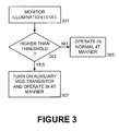
- Figure 3 is a flow diagram illustrating the method of operation of the 4T active pixel of Figure 2.
- Figure 4 shows an image sensor formed using the active pixels and methods of the present invention.
- Figure 1 illustrates a CMOS active pixel that uses four transistors. This is known in the art as a 4T active pixel.
- a light sensing element 101 outputs a signal that is used to modulate an amplification transistor 105.
- the light-sensing element 101 can be one of a variety of devices, including without limitation, photogates, photodiodes, pinned photodiodes, partially pinned photodiodes, etc.
- a transfer transistor 201 is used to transfer the signal output by the light-sensing element 101 to a floating node A, which is connected to the gate of the amplification transistor 105 (also known as a source-follower transistor).
- the light sensing element 101 In operation, during an integration period (also referred to as an exposure period), the light sensing element 101 generates charge which is held at the light sensing element 101 because transfer transistor 201 is off. After the integration period, the transfer transistor 201 is turned on to transfer the signal to the floating node A. After the signal has been transferred to floating node A, the transfer transistor 201 is turned off again for the start of a subsequent integration period. Thus, as seen, the transfer transistor 201 turns on and off periodically to transfer signal from each integration period to the floating node A.
- the signal on the floating node A is then used to modulate the amplification transistor 105.
- a row select transistor 107 is used as a means to address the pixel and to selectively read out the signal onto a column bit line 109.
- the reset transistor 103 resets the floating node A to a reference voltage, in this particular embodiment, V dd .
- the floating node A is designed to be relatively small. Floating node A is designed to be relatively small in order to achieve high transfer or conversion gain. However, in high illumination conditions, the amount of charge (signal) produced by the light-sensing element 101 may be greater than the capacity of the floating node A. This will result in saturation of the floating node A and reduced dynamic range, as well as reduced signal-to-noise ratio (SNR).
- SNR signal-to-noise ratio
- a 4T active pixel formed in accordance with the present invention is shown.
- the present invention allows the floating node A in a 4T active pixel to have a variable capacitance. This is accomplished by having one or more "auxiliary" capacitors attached to the floating node A.
- the auxiliary capacitor in one embodiment, is formed by a transistor 203.
- the transistor 203 When the auxiliary transistor 203 is turned “on” by having signal AUX high, the transistor 203 becomes a MOS capacitor with a relatively high capacitance (C A ) compared to the capacitance C F of the floating node A.
- the auxiliary transistor 203 is turned “off” by having signal AUX low, the transistor 203 still has a relatively low parasitic capacitance (C A ).
- the suitable size of the auxiliary transistor 203 is best determined by various design parameters, device characteristics, process parameters, and the end market for the image sensor. Further, although the supplemental capacitance is supplied in this embodiment by a transistor 203 operating as a MOS capacitor, other types of switchable capacitances are also within the scope of the present invention.
- the auxiliary transistor 203 Under high illumination light conditions, the auxiliary transistor 203 is turned on during the readout operation. This, in effect, increases the capacitance of the floating node A. However, in low-light conditions, the auxiliary transistor 203 is turned off and the floating node A maintains its relatively small capacitance.
- the illumination level incident to the image sensor (and thus pixels) is monitored.
- the output from the image sensor can be examined for its brightness level.
- nearly every image sensor has circuitry for automatic gain control and exposure control.
- the ambient light level can be determined.
- the processed output from the image sensor can be examined to determine the relative ambient lighting conditions.
- a dedicated light-sensitive device outside of the imaging area of the image sensor can be used to monitor the amount of incident light onto the image sensor.
- the illumination level determined at box 301 is compared to a threshold value.
- the threshold value is the trigger for turning on the auxiliary transistor 203.
- the precise point where the threshold is set may be made variable depending upon design considerations, parameters, and characteristics of the image sensor, and may even be adjustable at the discretion of the user of the image sensor.
- the auxiliary transistor 203 is turned on during operation. However, if the illumination level is lower than the threshold, then at box 305, the auxiliary transistor 203 is turned off.
- the floating node A In a 4T pixel, in order to obtain high transfer gain, the floating node A is designed to be relatively small and have a relatively small capacitance, for example, on the order of 2 femtofarads. If the image sensor and pixels use a one-volt signal range, this means that the maximum number of electrons (Q max ) that can be held at the floating node A is about 12,500. Considering "shot noise,” this results in a maximum signal-to-noise ratio of 112. However, in many illumination conditions, a light-sensing element, such as a pinned photodiode, may generate more signal (electrons) than Q max .
- an auxiliary capacitance in this embodiment the auxiliary transistor 203 is switched on during operation where there is relatively high ambient illumination. This results in the capacitance on the floating node A to increase, i.e., the sum of the "4T normal" floating node (2 femtofarads) and the capacitance provided by the auxiliary transistor 201.
- the total capacitance of the floating node is C F and C V , where C F is the capacitance of the floating node and C V is the capacitance of the auxiliary transistor 203.
- C F is the capacitance of the floating node
- C V is the capacitance of the auxiliary transistor 203.
- C V is merely the parasitic capacitance (referred to as C V1 ) between the gate and drain of the auxiliary transistor 203.
- C V is the MOS capacitance (referred to as C V2 ) of the auxiliary transistor 203.
- auxiliary transistor 203 only a single auxiliary transistor 203 is present.
- multiple auxiliary transistors in parallel or in series may be used to have gradations in controlling the capacitance of the floating node A and thus the conversion gain.
- any number of intermediate conversion gains can be obtained by appropriately controlling the cascade of auxiliary transistors.
- the capacitance of the floating node A is increased upon detection of a high level of illumination.
- the converse arrangement may also be implemented.
- "normal" operation may have the capacitance at floating node A be relatively high.
- the capacitance at floating node A may be decreased to improve conversion gain. This decrease may be done be turning off the auxiliary capacitance.
- a pixel and image sensor formed in accordance with the present invention has two modes of operation: a high illumination mode and a low illumination mode.
- the present invention switches on an auxiliary capacitance at the floating node based upon the amount of illumination on the image sensor.
- the amount of illumination on the image sensor can be determined in a variety of ways, and any method for determining the level of illumination could easily be applied to the present invention. Once the level of illumination is determined, a decision is made by comparing the level of illumination to a threshold whether to switch on the auxiliary capacitance (for high illumination) or not switch on the auxiliary capacitance (for low illumination).
- the active pixels described above may be used in a sensor array of a CMOS image sensor 1101.
- Figure 4 shows a CMOS image sensor formed in accordance with the present invention.
- the CMOS image sensor includes a sensor array 1103, a processor circuit 1105, an input/output (I/O) 1107, memory 1109, and bus 1111.
- I/O input/output
- memory 1109 memory
- bus 1111 bus 1111
- each of these components is formed on a single silicon substrate and manufactured to be integrated onto a single chip using standard CMOS processes.
- the sensor array 1103 portion may be, for example, substantially similar to the sensor arrays portions of image sensors manufactured by the assignee of the present invention, OmniVision Technologies, Inc., of Sunnyvale, CA, as model numbers OV561 0 or OV7640, except that the pixels are replaced with the active pixels disclosed herein.
Landscapes
- Engineering & Computer Science (AREA)
- Multimedia (AREA)
- Signal Processing (AREA)
- Solid State Image Pick-Up Elements (AREA)
- Transforming Light Signals Into Electric Signals (AREA)
Applications Claiming Priority (1)
| Application Number | Priority Date | Filing Date | Title |
|---|---|---|---|
| US10/986,616 US20060103749A1 (en) | 2004-11-12 | 2004-11-12 | Image sensor and pixel that has switchable capacitance at the floating node |
Publications (2)
| Publication Number | Publication Date |
|---|---|
| EP1657911A2 true EP1657911A2 (fr) | 2006-05-17 |
| EP1657911A3 EP1657911A3 (fr) | 2009-05-27 |
Family
ID=35929857
Family Applications (1)
| Application Number | Title | Priority Date | Filing Date |
|---|---|---|---|
| EP05256740A Withdrawn EP1657911A3 (fr) | 2004-11-12 | 2005-10-31 | Capteur d'image et pixel avec capacité connectable au noeud flottant |
Country Status (4)
| Country | Link |
|---|---|
| US (1) | US20060103749A1 (fr) |
| EP (1) | EP1657911A3 (fr) |
| CN (1) | CN1774032A (fr) |
| TW (1) | TWI286029B (fr) |
Cited By (2)
| Publication number | Priority date | Publication date | Assignee | Title |
|---|---|---|---|---|
| WO2011091785A1 (fr) * | 2010-01-28 | 2011-08-04 | Conti Temic Microelectronic Gmbh | Capteur d'image à dynamique élevée pour détecter de la lumière modulée |
| US9659983B2 (en) | 2011-07-15 | 2017-05-23 | Semiconductor Energy Laboratory Co., Ltd. | Semiconductor device and method for driving the same |
Families Citing this family (43)
| Publication number | Priority date | Publication date | Assignee | Title |
|---|---|---|---|---|
| US7427790B2 (en) * | 2007-01-19 | 2008-09-23 | Eastman Kodak Company | Image sensor with gain control |
| EP2126526A1 (fr) * | 2007-03-05 | 2009-12-02 | Arokia Nathan | Pixels de capteur, barrettes, systèmes de barrettes et procédés associés |
| US7915702B2 (en) * | 2007-03-15 | 2011-03-29 | Eastman Kodak Company | Reduced pixel area image sensor |
| US8159585B2 (en) | 2007-05-01 | 2012-04-17 | Omnivision Technologies, Inc. | Image sensor pixel with gain control |
| CN101330577B (zh) * | 2008-08-01 | 2010-04-07 | 李斌桥 | 可变换工作模式的cmos图像传感器 |
| US8233070B2 (en) * | 2009-03-27 | 2012-07-31 | International Business Machines Corporation | Variable dynamic range pixel sensor cell, design structure and method |
| GB0921354D0 (en) * | 2009-12-05 | 2010-01-20 | Univ Nottingham | Improvements in and relating to optical sensors and optical sensing |
| US8294077B2 (en) | 2010-12-17 | 2012-10-23 | Omnivision Technologies, Inc. | Image sensor having supplemental capacitive coupling node |
| TWI423673B (zh) * | 2011-03-17 | 2014-01-11 | Innolux Corp | 影像感測畫素及其驅動方法 |
| KR101294445B1 (ko) * | 2011-04-13 | 2013-08-07 | 엘지이노텍 주식회사 | 픽셀, 픽셀 어레이, 픽셀 어레이를 포함하는 이미지센서 및 픽셀 어레이의 구동방법 |
| US8643132B2 (en) | 2011-06-08 | 2014-02-04 | Omnivision Technologies, Inc. | In-pixel high dynamic range imaging |
| US8729451B2 (en) | 2011-08-30 | 2014-05-20 | Omnivision Technologies, Inc. | Multilevel reset voltage for multi-conversion gain image sensor |
| KR101930755B1 (ko) | 2012-03-21 | 2018-12-19 | 삼성전자주식회사 | 이미지 센서의 구동 방법 |
| US9276031B2 (en) | 2013-03-04 | 2016-03-01 | Apple Inc. | Photodiode with different electric potential regions for image sensors |
| US9741754B2 (en) | 2013-03-06 | 2017-08-22 | Apple Inc. | Charge transfer circuit with storage nodes in image sensors |
| JP6176062B2 (ja) * | 2013-11-06 | 2017-08-09 | ソニー株式会社 | 固体撮像装置およびその駆動方法、並びに電子機器 |
| US9762823B2 (en) * | 2013-11-18 | 2017-09-12 | Flir Systems, Inc. | Imager with increased readout capacitance |
| US9473706B2 (en) * | 2013-12-09 | 2016-10-18 | Apple Inc. | Image sensor flicker detection |
| US10285626B1 (en) | 2014-02-14 | 2019-05-14 | Apple Inc. | Activity identification using an optical heart rate monitor |
| US9686485B2 (en) | 2014-05-30 | 2017-06-20 | Apple Inc. | Pixel binning in an image sensor |
| CN104010142B (zh) * | 2014-06-12 | 2018-03-27 | 北京思比科微电子技术股份有限公司 | 有源像素及图像传感器及其控制时序 |
| CN104135633A (zh) * | 2014-08-25 | 2014-11-05 | 北京思比科微电子技术股份有限公司 | 可变转换增益的图像传感器像素及其工作方法 |
| US9467628B2 (en) * | 2014-08-26 | 2016-10-11 | Sensors Unlimited, Inc. | High dynamic range image sensor |
| US9456153B2 (en) * | 2015-01-18 | 2016-09-27 | Pixart Imaging (Penang) Sdn. Bhd. | Pixel image non-uniformity compensation method based on capacitance trimming and image sensor having pixels with variable capacitors for non-uniformity compensation |
| US11330206B2 (en) * | 2016-01-30 | 2022-05-10 | Pixart Imaging Inc. | Image sensing circuit and method capable of obtaining higher image brightness dynamic range |
| US10630918B2 (en) * | 2016-01-30 | 2020-04-21 | Pixart Imaging Inc. | Image sensing circuit and method capable of obtaining higher image brightness dynamic range |
| TWI646821B (zh) | 2016-01-30 | 2019-01-01 | 原相科技股份有限公司 | 可獲取較高影像亮度動態範圍的影像感測電路及方法 |
| US10438987B2 (en) | 2016-09-23 | 2019-10-08 | Apple Inc. | Stacked backside illuminated SPAD array |
| KR102678455B1 (ko) | 2016-12-30 | 2024-06-27 | 삼성전자주식회사 | 이미지 센서 |
| US10656251B1 (en) | 2017-01-25 | 2020-05-19 | Apple Inc. | Signal acquisition in a SPAD detector |
| JP6799690B2 (ja) | 2017-01-25 | 2020-12-16 | アップル インコーポレイテッドApple Inc. | 変調感度を有するspad検出器 |
| US10962628B1 (en) | 2017-01-26 | 2021-03-30 | Apple Inc. | Spatial temporal weighting in a SPAD detector |
| US10362255B2 (en) | 2017-02-09 | 2019-07-23 | Semiconductor Components Industries, Llc | Multi-conversion gain pixel configurations |
| US10622538B2 (en) | 2017-07-18 | 2020-04-14 | Apple Inc. | Techniques for providing a haptic output and sensing a haptic input using a piezoelectric body |
| US10440301B2 (en) | 2017-09-08 | 2019-10-08 | Apple Inc. | Image capture device, pixel, and method providing improved phase detection auto-focus performance |
| US11019294B2 (en) | 2018-07-18 | 2021-05-25 | Apple Inc. | Seamless readout mode transitions in image sensors |
| US10848693B2 (en) | 2018-07-18 | 2020-11-24 | Apple Inc. | Image flare detection using asymmetric pixels |
| US11563910B2 (en) | 2020-08-04 | 2023-01-24 | Apple Inc. | Image capture devices having phase detection auto-focus pixels |
| US11546532B1 (en) | 2021-03-16 | 2023-01-03 | Apple Inc. | Dynamic correlated double sampling for noise rejection in image sensors |
| US12192644B2 (en) | 2021-07-29 | 2025-01-07 | Apple Inc. | Pulse-width modulation pixel sensor |
| US12069384B2 (en) | 2021-09-23 | 2024-08-20 | Apple Inc. | Image capture devices having phase detection auto-focus pixels |
| CN116249028B (zh) * | 2021-12-07 | 2025-09-05 | 格科微电子(上海)有限公司 | 可变增益像素单元电路、hdr图像传感器 |
| CN117835074A (zh) * | 2022-09-23 | 2024-04-05 | 北京京东方光电科技有限公司 | 一种探测基板、其驱动方法及探测装置 |
Family Cites Families (21)
| Publication number | Priority date | Publication date | Assignee | Title |
|---|---|---|---|---|
| US5488415A (en) * | 1993-07-09 | 1996-01-30 | Olympus Optical Co., Ltd. | Solid-state image pickup device having a photoelectric conversion detection cell with high sensitivity |
| JPH08149376A (ja) * | 1994-11-18 | 1996-06-07 | Olympus Optical Co Ltd | 固体撮像装置 |
| US5900623A (en) * | 1997-08-11 | 1999-05-04 | Chrontel, Inc. | Active pixel sensor using CMOS technology with reverse biased photodiodes |
| US6246436B1 (en) * | 1997-11-03 | 2001-06-12 | Agilent Technologies, Inc | Adjustable gain active pixel sensor |
| US6512544B1 (en) * | 1998-06-17 | 2003-01-28 | Foveon, Inc. | Storage pixel sensor and array with compression |
| JP3592106B2 (ja) * | 1998-11-27 | 2004-11-24 | キヤノン株式会社 | 固体撮像装置およびカメラ |
| US6850278B1 (en) * | 1998-11-27 | 2005-02-01 | Canon Kabushiki Kaisha | Solid-state image pickup apparatus |
| US7009648B2 (en) * | 2000-02-22 | 2006-03-07 | Asulab S.A. | Method for operating a CMOS image sensor |
| JP3939092B2 (ja) * | 2000-12-28 | 2007-06-27 | セイコーインスツル株式会社 | 光電変換装置 |
| US20040036784A1 (en) * | 2002-08-23 | 2004-02-26 | Bock Nikolai E. | High dynamic range pixel with gain and true shutter capability |
| US7327393B2 (en) * | 2002-10-29 | 2008-02-05 | Micron Technology, Inc. | CMOS image sensor with variable conversion gain |
| US6903394B2 (en) * | 2002-11-27 | 2005-06-07 | Micron Technology, Inc. | CMOS imager with improved color response |
| KR100525895B1 (ko) * | 2003-04-30 | 2005-11-02 | 매그나칩 반도체 유한회사 | 씨모스 이미지 센서의 단위화소 |
| KR100523672B1 (ko) * | 2003-04-30 | 2005-10-24 | 매그나칩 반도체 유한회사 | 다중 플로팅디퓨젼영역을 구비하는 씨모스 이미지센서 |
| US7075049B2 (en) * | 2003-06-11 | 2006-07-11 | Micron Technology, Inc. | Dual conversion gain imagers |
| US7078746B2 (en) * | 2003-07-15 | 2006-07-18 | Micron Technology, Inc. | Image sensor with floating diffusion gate capacitor |
| US20050157194A1 (en) * | 2004-01-06 | 2005-07-21 | Altice Peter P.Jr. | Imager device with dual storage nodes |
| US7091531B2 (en) * | 2004-04-07 | 2006-08-15 | Micron Technology, Inc. | High dynamic range pixel amplifier |
| TWI264086B (en) * | 2004-06-04 | 2006-10-11 | Via Tech Inc | Method and apparatus for image sensor |
| US7193198B2 (en) * | 2004-10-01 | 2007-03-20 | Omnivision Technologies, Inc. | Image sensor and pixel that has variable capacitance output or floating node |
| US7242430B2 (en) * | 2004-11-03 | 2007-07-10 | Taiwan Semiconductor Manufacturing Co., Ltd. | High dynamic range image sensor cell |
-
2004
- 2004-11-12 US US10/986,616 patent/US20060103749A1/en not_active Abandoned
-
2005
- 2005-10-12 TW TW094135518A patent/TWI286029B/zh not_active IP Right Cessation
- 2005-10-31 EP EP05256740A patent/EP1657911A3/fr not_active Withdrawn
- 2005-11-14 CN CN200510124484.1A patent/CN1774032A/zh active Pending
Cited By (3)
| Publication number | Priority date | Publication date | Assignee | Title |
|---|---|---|---|---|
| WO2011091785A1 (fr) * | 2010-01-28 | 2011-08-04 | Conti Temic Microelectronic Gmbh | Capteur d'image à dynamique élevée pour détecter de la lumière modulée |
| US9659983B2 (en) | 2011-07-15 | 2017-05-23 | Semiconductor Energy Laboratory Co., Ltd. | Semiconductor device and method for driving the same |
| US10304878B2 (en) | 2011-07-15 | 2019-05-28 | Semiconductor Energy Laboratory Co., Ltd. | Semiconductor device and method for driving the same |
Also Published As
| Publication number | Publication date |
|---|---|
| CN1774032A (zh) | 2006-05-17 |
| TWI286029B (en) | 2007-08-21 |
| TW200621014A (en) | 2006-06-16 |
| EP1657911A3 (fr) | 2009-05-27 |
| US20060103749A1 (en) | 2006-05-18 |
Similar Documents
| Publication | Publication Date | Title |
|---|---|---|
| US20060103749A1 (en) | Image sensor and pixel that has switchable capacitance at the floating node | |
| US12231788B2 (en) | Method, apparatus, and system providing an imager with pixels having extended dynamic range | |
| US11595600B2 (en) | Method, apparatus and system providing a storage gate pixel with high dynamic range | |
| CN205566484U (zh) | 图像传感器像素和成像系统 | |
| KR100763442B1 (ko) | 듀얼 변환 이득 이미저 | |
| CN108470742B (zh) | Hdr图像传感器像素结构及成像系统 | |
| US7193198B2 (en) | Image sensor and pixel that has variable capacitance output or floating node | |
| US8130302B2 (en) | Methods and apparatus providing selective binning of pixel circuits | |
| US7990446B2 (en) | High dynamic range pixel amplifier | |
| US7956913B2 (en) | Image sensor and pixel that has positive transfer gate voltage during integration period | |
| US7889258B2 (en) | Dual sensitivity image sensor | |
| US8115841B2 (en) | Method, apparatus and system providing an image sensor having pixels with multiple exposures, diodes and gain readouts | |
| US8072524B2 (en) | Solid-state image-sensing device | |
| US7538304B2 (en) | Reducing noise in an imager by sampling signals with a plurality of capacitances connected to an output line | |
| US12538049B2 (en) | Ramp signal generator, image sensor, and auto-zero level control method for ramp signals | |
| US20070153109A1 (en) | Image sensor element with multiple outputs | |
| US20040085466A1 (en) | Digital pixel sensor with anti-blooming control | |
| WO2008010893A2 (fr) | Procédé, appareil et système de suppression de l'injection de charge dans des capteurs de pixels actifs | |
| US20200059612A1 (en) | Pixel apparatus and cmos image sensor using the same | |
| US20060268140A1 (en) | Method and apparatus for reducing noise in analog amplifier circuits and solid state imagers employing such circuits | |
| US20260019721A1 (en) | Image sensing device |
Legal Events
| Date | Code | Title | Description |
|---|---|---|---|
| PUAI | Public reference made under article 153(3) epc to a published international application that has entered the european phase |
Free format text: ORIGINAL CODE: 0009012 |
|
| AK | Designated contracting states |
Kind code of ref document: A2 Designated state(s): AT BE BG CH CY CZ DE DK EE ES FI FR GB GR HU IE IS IT LI LT LU LV MC NL PL PT RO SE SI SK TR |
|
| AX | Request for extension of the european patent |
Extension state: AL BA HR MK YU |
|
| PUAL | Search report despatched |
Free format text: ORIGINAL CODE: 0009013 |
|
| AK | Designated contracting states |
Kind code of ref document: A3 Designated state(s): AT BE BG CH CY CZ DE DK EE ES FI FR GB GR HU IE IS IT LI LT LU LV MC NL PL PT RO SE SI SK TR |
|
| AX | Request for extension of the european patent |
Extension state: AL BA HR MK YU |
|
| AKX | Designation fees paid |
Designated state(s): AT BE BG CH CY CZ DE DK EE ES FI FR GB GR HU IE IS IT LI LT LU LV MC NL PL PT RO SE SI SK TR |
|
| STAA | Information on the status of an ep patent application or granted ep patent |
Free format text: STATUS: THE APPLICATION IS DEEMED TO BE WITHDRAWN |
|
| 18D | Application deemed to be withdrawn |
Effective date: 20091128 |