EP1657965A2 - Dispositifs d'affichage flexibles - Google Patents
Dispositifs d'affichage flexibles Download PDFInfo
- Publication number
- EP1657965A2 EP1657965A2 EP05256963A EP05256963A EP1657965A2 EP 1657965 A2 EP1657965 A2 EP 1657965A2 EP 05256963 A EP05256963 A EP 05256963A EP 05256963 A EP05256963 A EP 05256963A EP 1657965 A2 EP1657965 A2 EP 1657965A2
- Authority
- EP
- European Patent Office
- Prior art keywords
- display
- gap
- electrode
- insulating layer
- conducting track
- Prior art date
- Legal status (The legal status is an assumption and is not a legal conclusion. Google has not performed a legal analysis and makes no representation as to the accuracy of the status listed.)
- Withdrawn
Links
Images

Classifications
-
- H—ELECTRICITY
- H05—ELECTRIC TECHNIQUES NOT OTHERWISE PROVIDED FOR
- H05B—ELECTRIC HEATING; ELECTRIC LIGHT SOURCES NOT OTHERWISE PROVIDED FOR; CIRCUIT ARRANGEMENTS FOR ELECTRIC LIGHT SOURCES, IN GENERAL
- H05B33/00—Electroluminescent light sources
- H05B33/12—Light sources with substantially two-dimensional [2D] radiating surfaces
- H05B33/14—Light sources with substantially two-dimensional [2D] radiating surfaces characterised by the chemical or physical composition or the arrangement of the electroluminescent material, or by the simultaneous addition of the electroluminescent material in or onto the light source
- H05B33/145—Arrangements of the electroluminescent material
-
- H—ELECTRICITY
- H05—ELECTRIC TECHNIQUES NOT OTHERWISE PROVIDED FOR
- H05B—ELECTRIC HEATING; ELECTRIC LIGHT SOURCES NOT OTHERWISE PROVIDED FOR; CIRCUIT ARRANGEMENTS FOR ELECTRIC LIGHT SOURCES, IN GENERAL
- H05B33/00—Electroluminescent light sources
- H05B33/12—Light sources with substantially two-dimensional [2D] radiating surfaces
- H05B33/22—Light sources with substantially two-dimensional [2D] radiating surfaces characterised by the chemical or physical composition or the arrangement of auxiliary dielectric or reflective layers
-
- H—ELECTRICITY
- H05—ELECTRIC TECHNIQUES NOT OTHERWISE PROVIDED FOR
- H05B—ELECTRIC HEATING; ELECTRIC LIGHT SOURCES NOT OTHERWISE PROVIDED FOR; CIRCUIT ARRANGEMENTS FOR ELECTRIC LIGHT SOURCES, IN GENERAL
- H05B33/00—Electroluminescent light sources
- H05B33/12—Light sources with substantially two-dimensional [2D] radiating surfaces
- H05B33/26—Light sources with substantially two-dimensional [2D] radiating surfaces characterised by the composition or arrangement of the conductive material used as an electrode
-
- H—ELECTRICITY
- H01—ELECTRIC ELEMENTS
- H01H—ELECTRIC SWITCHES; RELAYS; SELECTORS; EMERGENCY PROTECTIVE DEVICES
- H01H2219/00—Legends
- H01H2219/002—Legends replaceable; adaptable
- H01H2219/018—Electroluminescent panel
Definitions
- the present invention relates to flexible displays, particularly but not exclusively relating to flexible printed displays such as Electroluminescent (EL) displays.
- EL Electroluminescent
- Electroluminescence is the emission of light from a substance under electric-field excitation. Phosphor electroluminescence was discovered and documented in 1936, but it was not until the 1950s that GTE Sylvania received a patent for an EL powder lamp.
- a typical, known phosphor EL device is shown in Figure 1 of the accompanying drawings and comprises a light emitting material 3 in a dielectric matrix 5, sandwiched between two conducting electrodes 1, 6.
- the material comprises a light-emitting component (the "emitter") being phosphor, typically a zinc sulphide (ZnS) powder doped with manganese (Mn).
- the emitter typically a zinc sulphide (ZnS) powder doped with manganese (Mn).
- ZnS zinc sulphide
- Mn manganese
- silver- (Ag) or graphite-loaded screen-printable inks and indium tin oxide (ITO), which is a transparent conductive material are used as the electrodes 1, 6.
- ITO indium tin oxide
- phosphor EL lamps can be made very thin (less than 0.3mm); they are flat, fully flexible when applied to a flexible plastics substrate; they are rugged, have a wide viewing angle, can be made quite cheaply, can be made in low volumes using simple techniques, and give off very little heat when emitting light.
- EL lamps are used for backlighting LCD displays (for example, watches, mobile phones and so on) and instrument panels.
- discrete areas of the EL material can be made to emit light.
- display areas discrete areas of the EL material
- switches can be placed on the underside of the display (that is, the non-illuminated side) such that pressing on an area of the EL display, typically denoted by an illuminatable area as described above, flexes the display such that the switch is activated.
- Such a display can be seen in Figure 2 of the accompanying drawings.
- This has the substrate 11, ITO electrode 12 and EL material 13 common to the lamp of Figure 1.
- the display areas are formed by forming an insulating layer 14 having gaps 14a therein on the underside of the EL material 13 and forming a conductive electrode 15 over the gaps.
- the gaps in this insulating layer 14 define the shape of the display area.
- a further insulating layer 16 is applied over the electrode 15; the further insulating layer 16 itself having gaps 16a. These gaps allow conductive tracks 17 to be laid over the further insulating layer 16, to contact the electrode and so supply it with the necessary AC signal. Current may therefore pass from the conducting tracks, though the "vias" 19 formed by the gaps in the further insulating layer to the electrode. In general, it is desired to keep the conductive tracks of as small an area as possible, in order to decrease the amount of conductive material used. The gaps are larger than the conductive tracks crossing them, such that errors in alignment of the conductive track relative to the gap are tolerated.
- the conductive tracks can be used to supply a network of display areas which are to be illuminated together. Junctions over the gap of each display area allow the track to branch to travel to each area in turn.
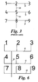
- Figure 3 of the accompanying drawings depicts schematically such a network that may be used on the numeric control panel of a domestic remote control; the number 1 to 9 are laid out in a 3x3 grid, with a central track 30 along the central column, and branches 31 out along each row from the central track.
- a flexible display comprising:
- the or each gap may be spaced along the surface of the display means from the centre of the display electrode. Preferably, the or each gap may be at the periphery of the display electrode, or outside the lit area thereof.
- the display may be further provided with a switch operated by flexure of the display means around the display electrode, in which the or each gap is spaced along the surface of the display means from the centre of the switch.
- the or each gap is positioned at the periphery of the switch, or in an even more preferred embodiment, outside the region of the display flexed when the switch is operated.
- the region to be flexed may be a non-planar region.
- the gaps may be outside this region.
- the non-planar section may be formed by subjecting the display to a strain force, generally at elevated temperature. The applicant has appreciated that avoiding having "vias" in this section avoids the undesirable increase in resistance.
- an electroluminescent display comprising:
- the conducting track over substantially the entirety of the or each gap has been shown to decrease the increase in resistance due to flexure of the "vias". The connection is made over a greater area, and as such the effect over the whole is reduced.
- the conducting track covers the entirety of the gap in the insulating layer.
- the conducting track may extend further around the or each gap such that a path for current is provided that does not pass over the gap. This may be provided by providing a larger area of track than gap (so that current may pass around the outside of the gap).
- a bypass track may be provided which branches off the track on one side of the or each gap and rejoins on a second side of the or each gap without passing over the or each gap.
- an electroluminescent display comprising:
- each segment terminates at a display electrode.
- the or each display electrode or the conducting track may be printed using conductive material with a resistivity of less than 0.5 ⁇ /square.
- the display may be manufactured so that the resistivity of the material does not vary significantly during manufacture of the display.
- the conductive material may be such that the resistance of the material does not vary significantly with aging due to the evolution of solvent from the conducting layer, or continuing chemical processes within the layer, such as cross linking of a binding matrix.
- the conductive material may be such that the resistance of the material does not vary significantly with deformations of the display that have a resultant radius of curvature of greater than 200mm or correspond to an actuation force of between 1g and 1kg.
- the display may be a printed display.
- the display is an electroluminescent display.
- the display means may be an electroluminescent material.
- the display may be a liquid crystal display, in which the display means may be a liquid crystal material.
- display area we mean a discrete section of the display that can be displayed or illuminated.
- an electronic device comprising the display of any of the previous aspects and associated electronic circuits.
- FIG. 1 shows a typical prior art EL lamp.
- the essential elements of the lamp are electroluminescent particles 3, such as phosphor, which are held between two electrodes 1,6.
- One of the electrodes is a transparent electrode 6, often of Indium Tin Oxide (ITO).
- ITO Indium Tin Oxide
- the particles 3 may be encapsulated in glass or ITO beads 4 and held in a dielectric matrix 5, to form a display means.
- a further layer of dielectric 2 may be provided in order to avoid short-circuiting problems and the whole lamp is laid out on a substrate 7 of some sort, typically glass or plastics. When an electric field is present between the two electrodes 1, 6, the EL lamp emits light 8.
- phosphor is used as an example of an electroluminescent material.
- electroluminescent material The person skilled in the art will appreciate that many other substances may be used for the same purpose without departing from the invention.
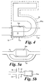
- the EL display shown in Figures 4 of the accompanying drawings forms an EL display of the number "5"; this is merely an example and any suitable number, letter or other device can be displayed.
- a clear substrate 11 forms a base for the display 10.
- a clear first electrode 12 typically of Indium Tin Oxide (ITO).
- a layer of electroluminescent (EL) material 13 is formed on top of this as is known in the prior art. This forms the display means of the present invention.
- an insulating layer 14 On top of the EL layer 13 is formed an insulating layer 14. This has a series of gaps 14a which define the shape of the illuminated display area; in this example the gap 14a would be in the shape of the figure "5".
- a display electrode 15 typically silver in a binder matrix. The display electrode 15 is arranged such that it covers the gap 14a and a wider area for convenient connection to the track discussed below.
- a further insulating layer 16 (corresponding to the insulating layer defined in the aspects of the invention), separating a conducting track (typically also printed as silver in a binding matrix) 17 on top of that layer from the display electrode 15.
- This insulating layer 16 also has gaps 16a therein to allow parts of the connecting track 17 - known as "vias" 19 - to connect to the display electrode 15. Electrical connection can then be made to the connecting track to a suitable power supply at a location remote to the display area.
- a switch 20 can be provided on the underside - that is the side opposite the substrate 11 through which light will be emitted - which a user can press by flexing the display 10. This is shown schematically in Figure 2 of the accompanying drawings.
- flexure of vias 19 causes an increase in resistance of the via and as such should be avoided. Rather than place the via in the centre of the digit shown, it is spaced outwards, in this case to the bottom left of the figure "5". This avoids the region of greatest flexure. Furthermore, rather than simply provide a track of constant width that passes over a section of the gap 16a in the further insulating layer 16, the conductive track 17 widens to cover the entire gap 16a. This increase in area reduces the overall effect of flexing of the vias 19.
- the widened section 17a also covers an area around the gap 16a. This provides a path for current to pass from one side of the gap to the other without passing through the via 19.
- the conductive track is provided with a separate bypass track 21 that splits from the conductive track 17 before it reaches the gap 16a and rejoins the conductive track on the other side of the track 17.
- the conductive track 17 branches over an area that is not over the gap 16a; one branch 22 terminates over the gap 16a whilst others 23, 24 continue to the display electrodes of other display areas.
- the other display areas would be the digits remaining from 1 to 9 as shown in Figure 6 of the accompanying drawings; the central track and branches are displaced from the prior art example of Figure 3 of the accompanying drawings such that the junctions between central track 60 and branches 61 are not over any of the gaps 16a. Not forming junctions over the gaps ensures that any increase in resistance of the vias does not affect the power supplied to any other display electrode.
Landscapes
- Electroluminescent Light Sources (AREA)
- Devices For Indicating Variable Information By Combining Individual Elements (AREA)
- Liquid Crystal (AREA)
Applications Claiming Priority (1)
| Application Number | Priority Date | Filing Date | Title |
|---|---|---|---|
| GB0425034A GB2420215A (en) | 2004-11-12 | 2004-11-12 | Flexible displays |
Publications (2)
| Publication Number | Publication Date |
|---|---|
| EP1657965A2 true EP1657965A2 (fr) | 2006-05-17 |
| EP1657965A3 EP1657965A3 (fr) | 2007-06-06 |
Family
ID=33523648
Family Applications (1)
| Application Number | Title | Priority Date | Filing Date |
|---|---|---|---|
| EP05256963A Withdrawn EP1657965A3 (fr) | 2004-11-12 | 2005-11-10 | Dispositifs d'affichage flexibles |
Country Status (5)
| Country | Link |
|---|---|
| US (1) | US20060103300A1 (fr) |
| EP (1) | EP1657965A3 (fr) |
| JP (1) | JP2006146198A (fr) |
| CN (1) | CN1779968A (fr) |
| GB (1) | GB2420215A (fr) |
Cited By (3)
| Publication number | Priority date | Publication date | Assignee | Title |
|---|---|---|---|---|
| US9632575B2 (en) | 2010-05-21 | 2017-04-25 | Nokia Technologies Oy | Method, an apparatus and a computer program for controlling an output from a display of an apparatus |
| US9823696B2 (en) | 2012-04-27 | 2017-11-21 | Nokia Technologies Oy | Limiting movement |
| US9823707B2 (en) | 2012-01-25 | 2017-11-21 | Nokia Technologies Oy | Contortion of an electronic apparatus |
Families Citing this family (1)
| Publication number | Priority date | Publication date | Assignee | Title |
|---|---|---|---|---|
| WO2009079004A1 (fr) | 2007-12-18 | 2009-06-25 | Lumimove, Inc., Dba Crosslink | Dispositifs et systèmes électroluminescents flexibles |
Family Cites Families (9)
| Publication number | Priority date | Publication date | Assignee | Title |
|---|---|---|---|---|
| US3514825A (en) * | 1966-04-04 | 1970-06-02 | Gen Co | Method of manufacturing electroluminescent display devices |
| US4532395A (en) * | 1983-09-20 | 1985-07-30 | Timex Corporation | Electroluminescent flexible touch switch panel |
| US6751898B2 (en) * | 1996-07-23 | 2004-06-22 | George W. Heropoulos | Electroluminescent display apparatus |
| GB9911789D0 (en) * | 1999-05-20 | 1999-07-21 | Cambridge Consultants | Electroluminescent devices |
| GB2371910A (en) * | 2001-01-31 | 2002-08-07 | Seiko Epson Corp | Display devices |
| US6876143B2 (en) * | 2002-11-19 | 2005-04-05 | John James Daniels | Organic light active devices and methods for fabricating the same |
| GB2404774B (en) * | 2003-08-07 | 2007-02-14 | Pelikon Ltd | Electroluminescent displays |
| US20050052128A1 (en) * | 2003-09-08 | 2005-03-10 | Polymatech Co. Ltd. | Light emitting electronic component |
| DE102005025224B3 (de) * | 2005-06-01 | 2006-10-26 | Daimlerchrysler Ag | Bedieneinheit, insbesondere für ein Fahrzeug |
-
2004
- 2004-11-12 GB GB0425034A patent/GB2420215A/en active Pending
-
2005
- 2005-11-07 JP JP2005322229A patent/JP2006146198A/ja active Pending
- 2005-11-10 EP EP05256963A patent/EP1657965A3/fr not_active Withdrawn
- 2005-11-11 CN CNA2005101194236A patent/CN1779968A/zh active Pending
- 2005-11-14 US US11/281,954 patent/US20060103300A1/en not_active Abandoned
Cited By (4)
| Publication number | Priority date | Publication date | Assignee | Title |
|---|---|---|---|---|
| US9632575B2 (en) | 2010-05-21 | 2017-04-25 | Nokia Technologies Oy | Method, an apparatus and a computer program for controlling an output from a display of an apparatus |
| US9983729B2 (en) | 2010-05-21 | 2018-05-29 | Nokia Technologies Oy | Method, an apparatus and a computer program for controlling an output from a display of an apparatus |
| US9823707B2 (en) | 2012-01-25 | 2017-11-21 | Nokia Technologies Oy | Contortion of an electronic apparatus |
| US9823696B2 (en) | 2012-04-27 | 2017-11-21 | Nokia Technologies Oy | Limiting movement |
Also Published As
| Publication number | Publication date |
|---|---|
| CN1779968A (zh) | 2006-05-31 |
| EP1657965A3 (fr) | 2007-06-06 |
| GB0425034D0 (en) | 2004-12-15 |
| GB2420215A (en) | 2006-05-17 |
| JP2006146198A (ja) | 2006-06-08 |
| US20060103300A1 (en) | 2006-05-18 |
Similar Documents
| Publication | Publication Date | Title |
|---|---|---|
| EP1080609B1 (fr) | Dispositifs electroluminescents | |
| CN101488064B (zh) | 触摸屏及利用了该触摸屏的可动接点体和开关 | |
| EP0917409B1 (fr) | Lampe électroluminescente et son procédé de production | |
| CN111682017B (zh) | 发光模块 | |
| US20100156276A1 (en) | Large-area oleds featuring homogeneous emission of light | |
| CN1379615A (zh) | 电致发光器件和使用该电致发光器件的照明装置 | |
| EP1657965A2 (fr) | Dispositifs d'affichage flexibles | |
| JP4981371B2 (ja) | 有機el素子 | |
| CN204809228U (zh) | 一种oled显示屏 | |
| KR20050025929A (ko) | 발광 전자 부품 | |
| JPH1140361A (ja) | El発光パネルおよびその製造方法 | |
| EP3509091B1 (fr) | Ensemble d'éclairage et dispositif d'éclairage | |
| CN1188298A (zh) | 一种平面显示器 | |
| CN102947968B (zh) | 亮度可变的平面发光体 | |
| KR100737932B1 (ko) | 이엘 램프시트 및 그의 제조 방법 | |
| US3531676A (en) | Electroluminescent cell for large area illumination | |
| US7872416B2 (en) | Electroluminescent display | |
| JP2011171068A (ja) | 表示装置 | |
| CN102110786A (zh) | 一种有机电致发光照明器件的布线方法 | |
| JP5425659B2 (ja) | 表示装置 | |
| JP2011174985A (ja) | 表示装置 | |
| CA2150875C (fr) | Module d'affichage electroluminescent a film mince | |
| US20060290643A1 (en) | Organic electroluminscent display device | |
| JP2002208490A (ja) | 積層型el素子ディスプレイ装置及びその製造方法。 | |
| KR100232173B1 (ko) | 전계 발광 디스플레이 패널 및 그 제조방법 |
Legal Events
| Date | Code | Title | Description |
|---|---|---|---|
| PUAI | Public reference made under article 153(3) epc to a published international application that has entered the european phase |
Free format text: ORIGINAL CODE: 0009012 |
|
| AK | Designated contracting states |
Kind code of ref document: A2 Designated state(s): AT BE BG CH CY CZ DE DK EE ES FI FR GB GR HU IE IS IT LI LT LU LV MC NL PL PT RO SE SI SK TR |
|
| AX | Request for extension of the european patent |
Extension state: AL BA HR MK YU |
|
| PUAL | Search report despatched |
Free format text: ORIGINAL CODE: 0009013 |
|
| AK | Designated contracting states |
Kind code of ref document: A3 Designated state(s): AT BE BG CH CY CZ DE DK EE ES FI FR GB GR HU IE IS IT LI LT LU LV MC NL PL PT RO SE SI SK TR |
|
| AX | Request for extension of the european patent |
Extension state: AL BA HR MK YU |
|
| 17P | Request for examination filed |
Effective date: 20071205 |
|
| 17Q | First examination report despatched |
Effective date: 20080109 |
|
| AKX | Designation fees paid |
Designated state(s): AT BE BG CH CY CZ DE DK EE ES FI FR GB GR HU IE IS IT LI LT LU LV MC NL PL PT RO SE SI SK TR |
|
| STAA | Information on the status of an ep patent application or granted ep patent |
Free format text: STATUS: THE APPLICATION IS DEEMED TO BE WITHDRAWN |
|
| 18D | Application deemed to be withdrawn |
Effective date: 20080520 |