EP1659600A2 - Elektrode für eine Farbstoffsolarzelle - Google Patents
Elektrode für eine Farbstoffsolarzelle Download PDFInfo
- Publication number
- EP1659600A2 EP1659600A2 EP05025202A EP05025202A EP1659600A2 EP 1659600 A2 EP1659600 A2 EP 1659600A2 EP 05025202 A EP05025202 A EP 05025202A EP 05025202 A EP05025202 A EP 05025202A EP 1659600 A2 EP1659600 A2 EP 1659600A2
- Authority
- EP
- European Patent Office
- Prior art keywords
- electrode
- substrate
- conductive
- conductive layer
- particles
- Prior art date
- Legal status (The legal status is an assumption and is not a legal conclusion. Google has not performed a legal analysis and makes no representation as to the accuracy of the status listed.)
- Granted
Links
Images


Classifications
-
- H—ELECTRICITY
- H10—SEMICONDUCTOR DEVICES; ELECTRIC SOLID-STATE DEVICES NOT OTHERWISE PROVIDED FOR
- H10F—INORGANIC SEMICONDUCTOR DEVICES SENSITIVE TO INFRARED RADIATION, LIGHT, ELECTROMAGNETIC RADIATION OF SHORTER WAVELENGTH OR CORPUSCULAR RADIATION
- H10F10/00—Individual photovoltaic cells, e.g. solar cells
-
- H—ELECTRICITY
- H01—ELECTRIC ELEMENTS
- H01G—CAPACITORS; CAPACITORS, RECTIFIERS, DETECTORS, SWITCHING DEVICES, LIGHT-SENSITIVE OR TEMPERATURE-SENSITIVE DEVICES OF THE ELECTROLYTIC TYPE
- H01G9/00—Electrolytic capacitors, rectifiers, detectors, switching devices, light-sensitive or temperature-sensitive devices; Processes of their manufacture
- H01G9/20—Light-sensitive devices
- H01G9/2022—Light-sensitive devices characterized by he counter electrode
-
- B—PERFORMING OPERATIONS; TRANSPORTING
- B82—NANOTECHNOLOGY
- B82Y—SPECIFIC USES OR APPLICATIONS OF NANOSTRUCTURES; MEASUREMENT OR ANALYSIS OF NANOSTRUCTURES; MANUFACTURE OR TREATMENT OF NANOSTRUCTURES
- B82Y10/00—Nanotechnology for information processing, storage or transmission, e.g. quantum computing or single electron logic
-
- H—ELECTRICITY
- H01—ELECTRIC ELEMENTS
- H01M—PROCESSES OR MEANS, e.g. BATTERIES, FOR THE DIRECT CONVERSION OF CHEMICAL ENERGY INTO ELECTRICAL ENERGY
- H01M4/00—Electrodes
- H01M4/86—Inert electrodes with catalytic activity, e.g. for fuel cells
- H01M4/8663—Selection of inactive substances as ingredients for catalytic active masses, e.g. binders, fillers
- H01M4/8668—Binders
-
- H—ELECTRICITY
- H01—ELECTRIC ELEMENTS
- H01M—PROCESSES OR MEANS, e.g. BATTERIES, FOR THE DIRECT CONVERSION OF CHEMICAL ENERGY INTO ELECTRICAL ENERGY
- H01M4/00—Electrodes
- H01M4/86—Inert electrodes with catalytic activity, e.g. for fuel cells
- H01M4/8663—Selection of inactive substances as ingredients for catalytic active masses, e.g. binders, fillers
- H01M4/8673—Electrically conductive fillers
-
- H—ELECTRICITY
- H01—ELECTRIC ELEMENTS
- H01M—PROCESSES OR MEANS, e.g. BATTERIES, FOR THE DIRECT CONVERSION OF CHEMICAL ENERGY INTO ELECTRICAL ENERGY
- H01M4/00—Electrodes
- H01M4/86—Inert electrodes with catalytic activity, e.g. for fuel cells
- H01M4/90—Selection of catalytic material
- H01M4/92—Metals of platinum group
- H01M4/928—Unsupported catalytic particles; loose particulate catalytic materials, e.g. in fluidised state
-
- H—ELECTRICITY
- H10—SEMICONDUCTOR DEVICES; ELECTRIC SOLID-STATE DEVICES NOT OTHERWISE PROVIDED FOR
- H10F—INORGANIC SEMICONDUCTOR DEVICES SENSITIVE TO INFRARED RADIATION, LIGHT, ELECTROMAGNETIC RADIATION OF SHORTER WAVELENGTH OR CORPUSCULAR RADIATION
- H10F77/00—Constructional details of devices covered by this subclass
- H10F77/20—Electrodes
-
- H—ELECTRICITY
- H01—ELECTRIC ELEMENTS
- H01G—CAPACITORS; CAPACITORS, RECTIFIERS, DETECTORS, SWITCHING DEVICES, LIGHT-SENSITIVE OR TEMPERATURE-SENSITIVE DEVICES OF THE ELECTROLYTIC TYPE
- H01G9/00—Electrolytic capacitors, rectifiers, detectors, switching devices, light-sensitive or temperature-sensitive devices; Processes of their manufacture
- H01G9/20—Light-sensitive devices
- H01G9/2027—Light-sensitive devices comprising an oxide semiconductor electrode
- H01G9/2031—Light-sensitive devices comprising an oxide semiconductor electrode comprising titanium oxide, e.g. TiO2
-
- H—ELECTRICITY
- H01—ELECTRIC ELEMENTS
- H01G—CAPACITORS; CAPACITORS, RECTIFIERS, DETECTORS, SWITCHING DEVICES, LIGHT-SENSITIVE OR TEMPERATURE-SENSITIVE DEVICES OF THE ELECTROLYTIC TYPE
- H01G9/00—Electrolytic capacitors, rectifiers, detectors, switching devices, light-sensitive or temperature-sensitive devices; Processes of their manufacture
- H01G9/20—Light-sensitive devices
- H01G9/2059—Light-sensitive devices comprising an organic dye as the active light absorbing material, e.g. adsorbed on an electrode or dissolved in solution
-
- H—ELECTRICITY
- H01—ELECTRIC ELEMENTS
- H01G—CAPACITORS; CAPACITORS, RECTIFIERS, DETECTORS, SWITCHING DEVICES, LIGHT-SENSITIVE OR TEMPERATURE-SENSITIVE DEVICES OF THE ELECTROLYTIC TYPE
- H01G9/00—Electrolytic capacitors, rectifiers, detectors, switching devices, light-sensitive or temperature-sensitive devices; Processes of their manufacture
- H01G9/20—Light-sensitive devices
- H01G9/2095—Light-sensitive devices comprising a flexible sustrate
-
- H—ELECTRICITY
- H10—SEMICONDUCTOR DEVICES; ELECTRIC SOLID-STATE DEVICES NOT OTHERWISE PROVIDED FOR
- H10K—ORGANIC ELECTRIC SOLID-STATE DEVICES
- H10K30/00—Organic devices sensitive to infrared radiation, light, electromagnetic radiation of shorter wavelength or corpuscular radiation
- H10K30/80—Constructional details
- H10K30/81—Electrodes
- H10K30/82—Transparent electrodes, e.g. indium tin oxide [ITO] electrodes
- H10K30/83—Transparent electrodes, e.g. indium tin oxide [ITO] electrodes comprising arrangements for extracting the current from the cell, e.g. metal finger grid systems to reduce the serial resistance of transparent electrodes
-
- H—ELECTRICITY
- H10—SEMICONDUCTOR DEVICES; ELECTRIC SOLID-STATE DEVICES NOT OTHERWISE PROVIDED FOR
- H10K—ORGANIC ELECTRIC SOLID-STATE DEVICES
- H10K85/00—Organic materials used in the body or electrodes of devices covered by this subclass
- H10K85/10—Organic polymers or oligomers
- H10K85/111—Organic polymers or oligomers comprising aromatic, heteroaromatic, or aryl chains, e.g. polyaniline, polyphenylene or polyphenylene vinylene
- H10K85/113—Heteroaromatic compounds comprising sulfur or selene, e.g. polythiophene
- H10K85/1135—Polyethylene dioxythiophene [PEDOT]; Derivatives thereof
-
- H—ELECTRICITY
- H10—SEMICONDUCTOR DEVICES; ELECTRIC SOLID-STATE DEVICES NOT OTHERWISE PROVIDED FOR
- H10K—ORGANIC ELECTRIC SOLID-STATE DEVICES
- H10K85/00—Organic materials used in the body or electrodes of devices covered by this subclass
- H10K85/20—Carbon compounds, e.g. carbon nanotubes or fullerenes
- H10K85/211—Fullerenes, e.g. C60
-
- H—ELECTRICITY
- H10—SEMICONDUCTOR DEVICES; ELECTRIC SOLID-STATE DEVICES NOT OTHERWISE PROVIDED FOR
- H10K—ORGANIC ELECTRIC SOLID-STATE DEVICES
- H10K85/00—Organic materials used in the body or electrodes of devices covered by this subclass
- H10K85/20—Carbon compounds, e.g. carbon nanotubes or fullerenes
- H10K85/221—Carbon nanotubes
-
- H—ELECTRICITY
- H10—SEMICONDUCTOR DEVICES; ELECTRIC SOLID-STATE DEVICES NOT OTHERWISE PROVIDED FOR
- H10K—ORGANIC ELECTRIC SOLID-STATE DEVICES
- H10K85/00—Organic materials used in the body or electrodes of devices covered by this subclass
- H10K85/60—Organic compounds having low molecular weight
- H10K85/615—Polycyclic condensed aromatic hydrocarbons, e.g. anthracene
-
- Y—GENERAL TAGGING OF NEW TECHNOLOGICAL DEVELOPMENTS; GENERAL TAGGING OF CROSS-SECTIONAL TECHNOLOGIES SPANNING OVER SEVERAL SECTIONS OF THE IPC; TECHNICAL SUBJECTS COVERED BY FORMER USPC CROSS-REFERENCE ART COLLECTIONS [XRACs] AND DIGESTS
- Y02—TECHNOLOGIES OR APPLICATIONS FOR MITIGATION OR ADAPTATION AGAINST CLIMATE CHANGE
- Y02E—REDUCTION OF GREENHOUSE GAS [GHG] EMISSIONS, RELATED TO ENERGY GENERATION, TRANSMISSION OR DISTRIBUTION
- Y02E10/00—Energy generation through renewable energy sources
- Y02E10/50—Photovoltaic [PV] energy
- Y02E10/542—Dye sensitized solar cells
-
- Y—GENERAL TAGGING OF NEW TECHNOLOGICAL DEVELOPMENTS; GENERAL TAGGING OF CROSS-SECTIONAL TECHNOLOGIES SPANNING OVER SEVERAL SECTIONS OF THE IPC; TECHNICAL SUBJECTS COVERED BY FORMER USPC CROSS-REFERENCE ART COLLECTIONS [XRACs] AND DIGESTS
- Y02—TECHNOLOGIES OR APPLICATIONS FOR MITIGATION OR ADAPTATION AGAINST CLIMATE CHANGE
- Y02E—REDUCTION OF GREENHOUSE GAS [GHG] EMISSIONS, RELATED TO ENERGY GENERATION, TRANSMISSION OR DISTRIBUTION
- Y02E60/00—Enabling technologies; Technologies with a potential or indirect contribution to GHG emissions mitigation
- Y02E60/30—Hydrogen technology
- Y02E60/50—Fuel cells
-
- Y—GENERAL TAGGING OF NEW TECHNOLOGICAL DEVELOPMENTS; GENERAL TAGGING OF CROSS-SECTIONAL TECHNOLOGIES SPANNING OVER SEVERAL SECTIONS OF THE IPC; TECHNICAL SUBJECTS COVERED BY FORMER USPC CROSS-REFERENCE ART COLLECTIONS [XRACs] AND DIGESTS
- Y02—TECHNOLOGIES OR APPLICATIONS FOR MITIGATION OR ADAPTATION AGAINST CLIMATE CHANGE
- Y02P—CLIMATE CHANGE MITIGATION TECHNOLOGIES IN THE PRODUCTION OR PROCESSING OF GOODS
- Y02P70/00—Climate change mitigation technologies in the production process for final industrial or consumer products
- Y02P70/50—Manufacturing or production processes characterised by the final manufactured product
Definitions
- the present invention relates to an electrode, a photoelectric conversion element, and a dye-sensitized solar cell.
- Dye-sensitized solar cells that have been developed by Michael Graetzel in Switzerland are attracting attention as new types of solar cells that enable a high conversion efficiency and are low in cost (see, for example, Japanese Patent No. 2664194; and Michael Graetzel, Nature, United Kingdom, 1991, vol. 737, p. 353).
- a working electrode is constructed by forming a porous film with oxide semiconductive fine particles (such as nanoparticles of titanium dioxide or the like) on a transparent conductive substrate, and then causing a sensitizing dye to be provided to this porous film.
- oxide semiconductive fine particles such as nanoparticles of titanium dioxide or the like
- This working electrode is used with a counter electrode where the working electrode faces the counter electrode, and the space between the two electrodes is filled with an electrolyte solution that contains a redox pair (such as I 2 /I 3 - ).
- Such a dye-sensitized solar cell functions as a photoelectric conversion element that converts light energy into electricity when oxide semiconductive fine particles are sensitized by a sensitizing dye that absorbs incident light, such as sun light, thereby generating an electromotive force between the working electrode and the counter electrode.
- a material for the counter electrode materials that promote the oxidation-reduction reaction of the redox couple on the surface of the electrode are desirable, and platinum is preferred.
- a conductive glass which has a conductive layer, such as a platinum layer, formed on the surface of the glass, has been widely used as a counter electrode.
- Methods for forming the platinum layer include vacuum film formation methods, such as sputter methods or evaporation methods, and wet film formation methods in which after applying a solution containing platinum, such as chloroplatinate solution, on the surface of the substrate, the platinum is freed by subjecting it to heat treatment (e.g., 200°C or higher).
- electrodes formed by the vacuum film formation methods suffer from low productivity and high facility cost, as described previously. Furthermore, another shortcoming is that it is difficult to obtain a platinum layer having a large effective area as compared to a porous film of a working electrode that is disposed on the opposite side.
- the wet film formation methods have difficulty in being applied to plastic substrates since heat treatment is required, as described above.
- the present invention was conceived in light of the above-described circumstances, and an object thereof is to provide an electrode and a photoelectric conversion element that can be manufactured at low cost and have an increased effective area.
- the present invention provides an electrode including a substrate, and a conductive layer containing carbon particles and a conductive binder for binding the carbon particles formed above the substrate, in which numerous spaces extending from a surface of the conductive layer are defined in the conductive layer.
- the carbon particles preferably contain nanoparticle-like carbon particles as a main component.
- the conductive binder preferably contains a conductive polymer as a main component.
- Examples of the conductive polymer include poly (3,4- ethylene dioxythiophene) and derivatives thereof.
- the present invention provides a photoelectric conversion element, including: an electrode including a substrate, and a conductive layer containing carbon particles and a conductive binder for binding the carbon particles formed above the substrate, in which spaces that communicate with a surface of the conductive layer are defined between the carbon particles.
- the present invention provides a dye-sensitized photovoltaic cell, including: an electrode including a substrate, and a conductive layer containing carbon particles and a conductive binder for binding the carbon particles formed above the substrate, in which spaces that communicate with a surface of the conductive layer are defined between the carbon particles.
- the present invention provides an electrode including: a substrate, and a conductive layer containing platinum particles and a conductive binder for binding the platinum particles formed above the substrate, in which spaces that communicate with a surface of the conductive layer are defined between the platinum particles.
- the platinum particles preferably contain nanoparticle-like platinum particles as a main component.
- the present invention provides a photoelectric conversion element, including: an electrode including a substrate, and a conductive layer containing platinum particles and a conductive binder for binding the platinum particles formed above the substrate, in which spaces that communicate with a surface of the conductive layer are defined between the platinum particles.
- the present invention provides a dye-sensitized photovoltaic cell, including: an electrode including a substrate, and a conductive layer containing platinum particles and a conductive binder for binding the platinum particles formed above the substrate, in which spaces that communicate with a surface of the conductive layer are defined between the platinum particles.
- the electrode of the present invention it is possible to manufacture an electrode exhibiting stable properties with simplified steps at low cost. Furthermore, by binding the carbon particles with the conductive binder, it is possible to form an electrode with a porous structure having spaces on the surface thereof, thereby increasing the effective area (surface area) of the electrode. Furthermore, it is possible to form the conductive layer without requiring heat treatment at a high temperature. Thus, even when a base material with low heat resistance, such as one made from plastic, is used for the substrate, it is possible to prevent problems, such as degradation of the base material, Furthermore, by binding the platinum particles using the conductive binder, it is possible to form an electrode with a porous structure having spaces on the surface thereof, thereby increasing the effective area (surface area) of the electrode.
- the photoelectric conversion element of the present invention since the effective area (surface area) of the surface of the electrode is increased, it is possible to obtain excellent photoelectric conversion efficiency.
- the dye-sensitized solar cell of the present invention since incident light is sensitized by the sensitizing dye, it is possible to easily convert the light energy into electricity. In addition, since the effective area (surface area) of the electrode itself is increased, it is possible to obtain excellent photoelectric conversion efficiency.
- FIG. 1A is a cross-sectional view illustrating one example of an electrode according to a first exemplary embodiment of the present invention.
- An electrode also referred to as an electrode substrate
- An electrode substrate 1 includes, for example, a substrate 2 and a conductive layer 3 that contains carbon particles and a conductive binder for binding the carbon particles provided on the substrate 2.
- Examples of the substrate 2 include, but are not particularly limited to, a sheet or plate made of carbon, a glass, a plastic, a metal, a ceramic, or the like.
- Glasses that may be used as the substrate 2 include, for example, borosilicate glass, quartz glass, soda glass, phosphate glass, and the like.
- Plastics that may be used as the substrate 2 include, for example, polyethylene terephthalate (PET), polyethylene naphthalate (PEN), polybutylene terephthalate (PBT), a polyimide, and the like.
- Metals that may be used as the substrate 2 include, for example, titanium, nickel, and the like.
- the substrate 2 may be provided with a second conductive layer (not shown) made of a conductive metal oxide, such astin-doped indium oxide (ITO), fluorine-doped tin oxide (FTO), or FTO/ITO, or a metal formed on the surface above which the conductive layer 3 is to be provided.
- a conductive metal oxide such astin-doped indium oxide (ITO), fluorine-doped tin oxide (FTO), or FTO/ITO
- the material constituting the substrate and the second conductive layer is an exemplary material that is resistant to an electrolyte when in contact with the electrolyte.
- copper and silver are not suitable, for example, since they are attacked by iodine and easily dissolve into the electrolyte.
- the conductive layer 3 contains carbon particles and a conductive binder for binding the carbon particles, and spaces which communicate with a surface 3a of the conductive layer 3 are defined between the carbon particles.
- numerous spaces extending from a surface of the conductive layer 3 are defined in the conductive layer 3, stated differently, numerous spaces extending from a surface of the conductive layer 3 in the direction of the depth are defined between the carbon particles, and the numerous spaces define paths through which an electrolyte infiltrates.
- exemplary carbon particles are, but are not particularly limited to, nanoparticle-like ones from the viewpoint of film forming properties and surface area, and carbon particles having good conductivity are exemplary.
- nanoparticle-like particles of the present invention means that the particles have a diameter in either a major or a minor axis of 1000 nm or less. Any carbon nanotubes, carbon fibers, carbon nanohoms, or the like, with a length in the longitudinal direction of more than 1000 nm can be regarded as nanoparticle-like particles of the present invention provided that the minor axis diameter thereof is 1000 nm or less.
- nanoparticle-like carbon particles include particles, such as carbon nanotubes, carbon fibers, carbon nanohoms, carbon black, fullerenes, and the like. These materials may be prepared using well-known methods, or commercially available products may be used.
- carbon nanotube examples include single-wall carbon nanotubes (SWCNT) having a single layer of a graphene sheet and multi-wall carbon nanotubes (MWCNT) having multiple layers (two or more layers) of graphene sheets, which can be suitably used for the present invention.
- SWCNT single-wall carbon nanotubes
- MWCNT multi-wall carbon nanotubes
- a ketjen black may be used as carbon black.
- C 60 and C 70 fullerenes may be used.
- carbon particles are bound by a conductive binder in order to form a film of the carbon particles above the substrate 2.
- the conductive binder is preferably one that requires no high temperature treatment and is easily applied to form a film, and a conductive polymer is preferred from the viewpoint of these properties.
- Examples of conductive polymers include, for example, polythiophenes, polyanilines, polypyrroles, and derivatives of these.
- a single conductive polymer may be used alone, or a combination of several conductive polymers may be used as a conductive binder.
- thiophenes and derivatives thereof a thiophene having unsubstituted hydrogen atoms on the thiophene ring, or thiophenes having, for example, one or more of substituent alkyl groups, halogen atoms, alkoxy groups, cyano groups or the like, may be used.
- Poly (3- alkylthiophene), poly (3,4- dialkyl thiophene), and poly (3,4- alkylene dioxythiophene), such as poly (3,4- ethylene dioxythiophene) (PEDOT), are exemplary,
- polypyrroles and derivatives thereof polypyrroles with unsubstituted hydrogen atoms on the pyrrole ring, or polypyrroles having, for example, one or more of substituent alkyl groups, halogen atoms, alkoxy groups, cyano groups or the like may be used, Poly (3-alkyl pyrrole), poly (3,4- dialkyl pyrrole), and poly (3,4- alkylene dioxypyrrole), or the like are exemplary.
- polyanilines and derivatives thereof polyanilines, poly (N-alkyl aniline), poly (arylamine), poly (phenylenediamine), and poly (aminopyrene), or the like are exemplary.
- the spaces are cavities that communicate with the surface 3a of the conductive layer 3, and the spaces define paths through which an electrolyte (an electrolytic solution or the like) infiltrates.
- an electrolyte an electrolytic solution or the like
- the electrolyte infiltrates inside the spaces, and the entire inner surfaces of the spaces can function as an effective area that contributes to charge transfer, reaction, and the like.
- carbon nanoparticles having a large apparent volume per weight are exemplary as the spaces are formed effectively if these are used.
- a film of the carbon particles are formed using the conductive binder, it is possible to form the conductive layer 3 without requiring heat treatment at a high temperature, allowing formation of the film on a base material, such as one made of plastic, with low heat resistance.
- binder When carbon nanoparticles that have a large apparent volume per weight are used, a relatively large amount of binder is required in order to improve the film formation properties and the film strength. For this reason, when an insulating resin, such as polyester, polyurethane, polyvinylidene fluoride (PVdF), polyvinylidene fluoride-hexafluoropropylene copolymer (PVdF-HFP), or the like is used as a binder, the binder inhibits the particles from coming into contact with each other, which may reduce the conductivity of the electrode 1. The amount to be added and the mixed state of the binder may be difficult to control.
- PVdF polyvinylidene fluoride
- PVdF-HFP polyvinylidene fluoride-hexafluoropropylene copolymer
- the use of a binder that exhibits conductivity is advantageous in that decrease in the conductivity due to presence of the binder between particles is prevented and an increase in the internal resistance is suppressed.
- constraints in terms of the composition and the mixing method of the conductive layer 3 are few.
- the compounding ratio of the carbon particles to the conductive binder is appropriately selected according to types of carbon particles and conductive binder used. If too many carbon particles are present with respect to the amount of the conductive binder, the carbon particles may not be bound and a film may not be formed. Thus, the conductive binder is added at a compounding ratio such that the carbon particles are favorably bound to each other. If the amount of the carbon particles is too small with respect to the amount of the conductive binder, the carbon particles may be buried in the conductive binder and no spaces may be formed. Thus, the conductive binder is added at a compounding ratio such that spaces are formed.
- the compounding ratio of the carbon particles to the conductive binder is not particularly limited, but the value obtained by dividing the mass of the carbon particles by the mass of the conductive binder (i.e., the mass ratio of carbon/binder) is, for example, within a range from 0.5 to 5, or within a range from 1 to 2.
- the method for forming the electrode 1 of the present invention is not particularly limited, but the conductive layer 3 may be formed by dispersing or dissolving the carbon particles and the conductive binder into a solvent, applying the resulting mixture onto the substrate 2, and drying it, for example.
- the method for applying the mixture is not particularly limited, and various coating methods may be applicable, such as the doctor blade method, the spin coating method, the dipping method, the printing method, and the like.
- the solvent examples include, but not particularly limited to, tetrahydrofuran, ethyl methyl ketone, dimethylformamide, acetonitrile, methoxy acetonitrile, propionitrile, propylene carbonate, a diethyl carbonate, methanol, ⁇ - butyrolactone, and N-methylpyrrolidone.
- the carbon particles and the conductive binder be dispersed or dissolved in the solvent as evenly as possible, and the selection of the solvent is preferably made by taking the dispersibility and the solubility of the carbon particles and the conductive binder into consideration. It is desirable that the conductive binder have sufficient solubility or dispersibility with respect to the solvent.
- an electrode having stable properties can be readily manufactured without using platinum. Furthermore, by binding the carbon particles with the conductive binder, it is possible to form the conductive layer 3 with a porous structure having spaces on the surface 3a thereof, thereby increasing the effective area (surface area) of the electrode 1. Furthermore, it is possible to form the conductive layer 3 without requiring heat treatment at a high temperature. Thus, even when a base material with a low heat resistance, such as one made from plastic, is used for the substrate 2, it is possible to prevent problems such as degradation of the base material.
- a photoelectric conversion element 10 shown in FIG. 1B is a dye-sensitized solar cell having the electrode 1 shown in FIG. 1A as a counter electrode.
- This dye-sensitized solar cell 10 includes a transparent electrode substrate 6, a working electrode 8 having an oxide semiconductive porous film 7 made of oxide semiconductive fine particles formed on the transparent electrode substrate 6, and a counter electrode 1 provided facing the working electrode 8.
- a sensitizing dye is provided on the oxide semiconductive porous film 7, and an electrolyte layer 9 containing a redox couple is disposed between the working electrode 8 and the counter electrode 1.
- the transparent electrode substrate 6 used for the working electrode 8 may be prepared by forming a conductive layer 5 made of a glass plate, a plastic sheet, or the like, on a transparent base material 4 made of a conductive material. Having such a structure, the transparent electrode substrate 6 can function as a window through which light is introduced from outside.
- the transparent base material 4 is preferably made of a material having excellent optical transparence properties when taking its function into consideration.
- transparent plastic sheets made of polyethylene terephthalate (PET), polyethylene naphthalate (PEN), polycarbonate (PC), polyether sulfone (PES), or the like; a polished plate of a ceramic, such as titanium oxide, alumina, or the like, may be used.
- oxide semiconductors having excellent transparence properties such as ITO, tin oxide (SnO 2 ), FTO, or the like can be used either alone or in a mixture of two or more thereof when taking the light transmittance of the transparent electrode substrate 6 into consideration.
- the material is not limited, and any suitable material having light transmittance and conductivity appropriate for use in the conductive layer 5 may be used.
- a metal wiring layer made of gold, silver, platinum, aluminum, nickel, titanium, or the like may be used in combination with the transparent conductive layer provided that an area ratio of the metal wiring layer is within the range that does not significantly degrade the light transmittance of the transparent electrode substrate 6.
- the metal wiring layer preferably has a grid-like, stripe-like, or comb-like pattern so that light is transmitted through the transparent electrode substrate 6 as evenly as possible.
- the method used to form the conductive layer 5 on the transparent base material 4 is not particularly limited, and examples thereof include any known thin film formation methods, such as sputtering methods, or CVD methods, spray decomposition methods (SPD), or evaporation methods when the conductive layer 5 is formed from a metal semiconductive material, such as ITO.
- any known thin film formation methods such as sputtering methods, or CVD methods, spray decomposition methods (SPD), or evaporation methods when the conductive layer 5 is formed from a metal semiconductive material, such as ITO.
- the oxide semiconductive porous film 7 is a porous thin layer containing as a main component oxide semiconductive fine particles that are made of titanium oxide (TiO 2 ), tin oxide (SnO 2 ), tungsten oxide (WO 3 ), zinc oxide (ZnO), and niobium oxide (Nb 2 O 5 ), used either alone or in a combination of two or more materials, and have an average particle diameter of between 1 nm to 1000 nm.
- the method for forming the oxide semiconductive porous film 7 is not particularly limited, and it can be formed, for example, by employing methods such as a method in which a dispersion solution that is obtained by dispersing commercially available oxide semiconductive fine particles in a desired dispersion medium, or a colloid solution that can be prepared using a sol-gel method is applied, after desired additives have been added thereto if these are required, using a known coating method such as a screen printing method, an inkjet printing method, a roll coating method, a doctor blade method, a spin coating method, a spray coating method, or the like.
- Other methods include; a migration electrodeposition method in which the transparent electrode substrate 6 is immersed in colloid solution and oxide semiconductive fine particles are made to adhere to the transparent electrode substrate 6 by electrophoresis; a method in which a foaming agent is mixed in a colloid solution or dispersion solution which is then coated and baked so as to form a porous material; and a method in which polymer microbeads are mixed together and applied, and these polymer microbeads are then removed by thermal treatment or chemical treatment, so as to define spaces and thereby form a porous material.
- the dye that is provided in the oxide semiconductive porous film 7 is not particularly limited, and it is possible to use ruthenium complexes or iron complexes containing bipyridine structures, terpyridine structures, and the like in a ligand; metal complexes such as porphyrin and phthalocyanine; as well as organic dyes such as eosin, rhodamine, and melocyanine.
- the dye can be selected according to the application and the semiconductor that is used for the oxide semiconductive porous film 7.
- the electrolyte solution that is used for the electrolyte layer 9 it is possible to use an organic solvent or an ionic liquid (room temperature molten salt) that contains a redox pair. Furthermore, it is also possible to use what is known as a "gel electrolyte" which is quasi-solidified to reduce flowability and is obtained by adding a suitable gelling agent into the electrolyte solution. Furthermore, a polymer solid electrolyte or the like having electron transfer capability may be used.
- organic solvent examples include acetonitrile, methoxy acetonitrile, propionitrile, propylene carbonate, diethyl carbonate, and ⁇ - butyrolacton.
- the ionic liquid examples include salts made of cations, such as quaternary imidazolium based cations and anions, such as iodide ions or bistrifluoromethyl sulfonylimido anions, dicyanoamide anions, and the like.
- an electrolyte composition containing an ionic liquid and metal oxide particles and/or conductive particles may be used, as described in Japanese Patent Application No. 2003-347193 of the present applicant, for example.
- the metal oxide particles contained in the gel-form electrolyte may be one member or a mixture of two or members selected from the group consisting of TiO 2 , SnO 2 , WO 3 , ZnO, ITO, BaTiO 3 , Nb 2 O 5 , In 2 O 3 , ZrO 2 , Ta 2 O 5 , La 2 O 3 , SrTiO 3 , Y 2 O 3 , Ho 2 O 3 , Bi 2 O 3 , CeO 2 , and Al 2 O 3 .
- the metal oxide may be an oxide doped with a dopant, or a composite oxide.
- the conductive particles may be particles including carbon as a main component, and a specific example includes carbon-cased particles, such as carbon nonotubes, carbon fibers, carbon black, carbon nanohorns, or the like.
- the redox pair that is contained in the electrolyte layer 9 is not particularly limited.
- pairs such as iodine/iodide ions, bromine/bromide ions, and the like may be added.
- Additives such as tert -butylpyridine and the like can be added if necessary to this electrolyte solution.
- the method for forming the electrolyte layer 9 made of the electrolyte composition between the working electrode 8 and the counter electrode 1 is not particularly limited. Examples include, for example, a method in which the working electrode 8 and the counter electrode 1 are disposed facing each other and the electrolyte is supplied between the electrode 1 and 8 to form the electrolyte layer 9, or a method in which the electrolyte is dropped or applied on the counter electrode 1 or the working electrode 8 to form the electrolyte layer 9 and another electrode is stacked on the electrolyte layer 9.
- the gap between the working electrode 8 and the counter electrode 1 be sealed using a film if necessary, or that the working electrode 8, the electrolyte layer 9, and the counter electrode 1 be contained in an appropriate casing.
- the photoelectric conversion element 10 of this example has the above-described electrode, the effective area (surface area) of the surface of the electrode is increased and excellent photoelectric conversion efficiency can be obtained without using platinum.
- Carbon particles and a conductive binder in a composition listed in Table 1 were dissolved and dispersed in a solvent. After the resultant liquid material was applied to a substrate using a doctor blade, the coated material was thoroughly dried, thereby obtaining an electrode to be used as a counter electrode.
- Carbon particles and an insulative binder in a composition listed in Table 1 were dissolved and dispersed in a solvent. After the resultant liquid material was applied to a substrate using a doctor blade, the coated material was thoroughly dried, thereby obtaining an electrode to be used as a counter electrode. A commercially available glass having an FTO film formed thereon was used as the substrate.
- PVdF-HFP represents polyvinylidene fluoride-hexafluoropropylene copolymer.
- Examples 1-1 to 1-8 and Comparative Examples 1-1 to 1-3 were visually inspected for possible peel-off of the conductive layer, and the results were evaluated using the following three ranks: A, B, and C, wherein “A” means that no peeling off of the conductive layer was observed, “B” means that slight peeling off was observed, and “C” means that considerable peeling off was observed.
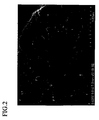
- Electron micrographs of the surface of the electrode having conductive layer that was made of carbon nanotubes and PEDOT are shown in FIGS. 2 and 3, An electron micrograph of a surface of a glass and a platinum layer formed above the glass by sputtering, in which the glass has an FTO film formed thereon, is shown in FIG. 4
- FIGS. 2 and 3 FIGS. 2 and 3 (FIG. 3 is a magnified picture of the center portion of the picture of FIG 2), it was confirmed that a matrix of carbon nanotubes was bound by a binder polymer in a conductive layer in the case in which the carbon nanotubes were bound by the conductive polymer. In addition, numerous spaces extending from the surface of the conductive layer in the direction of the depth were formed, and the carbon nonotubes were exposed in a large area. At the portions bound by the binder polymer, the carbon nonotubes were covered by the binder polymer.
- both the portion in which the carbon nonotubes are exposed and the portion covered by the binder polymers on the surface of the electrode can function as effective areas that contribute to charge transfer, reaction, and the like.
- Dye-sensitized photovoltaic cells having the electrodes of Examples 1-1 to 1-8 and Comparative Example 1-3 as counter electrodes were manufactured using the following procedures.
- the transparent electrode substrate 6 having the oxide semiconductive porous film 7 formed thereon was then immersed overnight in a dye solution so as to be sensitized by the dye to form a working electrode.
- a ruthenium bipyridine complex an N3 dye
- An ionic liquid based electrolytic solution prepared as follows was used as the electrolytic solution.
- the electrolytic solution was prepared by using 1-hexyl-3-methylimidazolium iodide (HMIm-I) as the ionic liquid and adding appropriate amounts of lithium iodide, iodine, and 4- tert -butylpyridine to the ionic liquid.
- HMIm-I 1-hexyl-3-methylimidazolium iodide
- the working electrode 8 was stacked on the counter electrode 1, and the electrolytic solution was supplied between the electrodes to form a dye-sensitized solar cell 10 that was a test cell.
- the photoelectric conversion characteristics of the cells were evaluated under light irradiating conditions of an AM (air mass) of 1.5 and an irradiance of 100 mW/cm 2 .
- each of the electrodes of Examples 1-1 to 1-8 exhibited characteristics comparative or even superior to those of the glass having a platinum layer. Furthermore, as indicated by Example 1-8, it is possible to obtain an excellent electrode and a dye-sensitized photovoltaic cell even when the first embodiment of the present invention is applied to a plastic substrate.
- Comparative Example 1-2 when carbon particles were bound using PVdF-HFP that is an insulative binder, the conductivity of the electrode was degraded since the electric connections between the carbon particles is inhibited by the insulating resin, resulting in a reduction in the photoelectric conversion efficiency. Furthermore, as indicated by Comparative Example 1-3, when the amount of the binder with respect to the amount of the carbon particles was reduced in order to improve the electric connection between the carbon particles in the case in which an insulative binder was used, a slight improvement in the photoelectric conversion efficiency was obtained although this was still inferior to those of the Examples. In addition, the coated film became unstable and was easily peeled off since the film strength of the conductive layer was degraded.
- the electrode according to the first embodiment of the present invention has a larger electrode surface area as well as higher conductivity, it was confirmed that it shows favorable photoelectric conversion characteristics when applied as a counter electrode of a dye-sensitized solar cell.
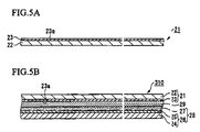
- FIG. 5A is a cross-sectional view illustrating one example of an electrode according to a second exemplary embodiment of the present invention.
- An electrode (also referred to as an electrode substrate) 21 includes, for example, a substrate 22 and a conductive layer 23 that contains platinum particles and a conductive binder for binding the platinum particles provided on the substrate 22.
- Examples of the substrate 22 include, but are not particularly limited to, a sheet or plate made of carbon, a glass, a plastic, a metal, a ceramic, or the like.
- Glasses that may be used as the substrate 22 include, for example, borosilicate glass, quartz glass, soda glass, phosphate glass, and the like.
- Plastics that may be used as the substrate 22 include, for example, polyethylene terephthalate (PET), polyethylene naphthalate (PEN), polybutylene terephthalate (PBT), a polyimide, and the like.
- Metals that may be used as the substrate 22 include, for example, titanium, nickel, and the like.
- the substrate 22 may be provided with a second conductive layer (not shown) made of a conductive metal oxide, such astin-doped indium oxide (ITO), fluorine-doped tin oxide (FTO), or FTO/ITO, or a metal formed on the surface above which the conductive layer 23 is to be provided.
- a conductive metal oxide such astin-doped indium oxide (ITO), fluorine-doped tin oxide (FTO), or FTO/ITO
- the material constituting the substrate and the second conductive layer is an exemplary material that is resistant to an electrolyte when in contact with the electrolyte.
- copper and silver are not suitable, for example, since they are attacked by iodine and easily dissolve into the electrolyte.
- the conductive layer 23 contains platinum particles and a conductive binder for binding the platinum particles, and spaces which communicate with a surface 3a of the conductive layer 3 are defined between the platinum particles.
- the platinum particles of the present invention can be, but are not particularly limited to, nanoparticle-like ones from the viewpoint of film forming properties and surface area, and platinum particles having good conductivity are exemplary.
- nanoparticle-like particles of the present invention means that the particles have a diameter in either main axis of 1000 nm or less. Fiber-like particles having a length more than 1000 nm in the longitudinal direction or spike-like particles having spikes having a length more than 1000 nm on the surface thereof can be regarded as nanoparticle-like particles of the present invention.
- platinum particles of spherical, polygonal, fiber-like, tree-needle-like, spike-like, flake-like, or porous particles, or the like may be used either alone or in combination.
- tree-needle-like particles, spike-like particles, and porous particles having a large surface area are preferred.
- platinum particles are bound by a conductive binder in order to form a film of the platinum particles above the substrate 22.
- the conductive binder is preferably one that requires no high temperature treatment and is easily applied to form a film, and a conductive polymer is preferred from the viewpoint of these properties.
- Examples of conductive polymers include, for example, polythiophenes, polyanilines, polypyrroles, and derivatives of these.
- a single conductive polymer may be used alone, or a combination of several conductive polymers may be used as a conductive binder.
- thiophenes and derivatives thereof a thiophene having unsubstituted hydrogen atoms on the thiophene ring, or thiophenes having, for example, one or more of substituent alkyl groups, halogen atoms, alkoxy groups, cyano groups or the like, may be used.
- Poly (3- alkylthiophene), poly (3,4- dialkyl thiophene), and poly (3,4- alkylene dioxythiophene), such as poly (3,4- ethylene dioxythiophene) (PEDOT), are exemplary.
- polypyrroles and derivatives thereof polypyrroles with unsubstituted hydrogen atoms on the pyrrole ring, or polypyrroles having, for example, one or more of substituent alkyl groups, halogen atoms, alkoxy groups, cyano groups or the like may be used.
- Poly (3-alkyl pyrrole), poly (3,4- dialkyl pyrrole), and poly (3,4- alkylene dioxypyrrole), or the like are exemplary.
- polyanilines and derivatives thereof polyanilines, poly (N-alkyl aniline), poly (arylamine), poly (phenylenediamine), and poly (aminopyrene), or the like are exemplary.
- the spaces are cavities that communicate with the surface 23a of the conductive layer 23, and the spaces define paths through which an electrolyte (an electrolytic solution or the like) infiltrates.
- an electrolyte an electrolytic solution or the like
- the electrolyte infiltrates inside the spaces, and the entire inner surfaces of the spaces can function as an effective area that contributes to charge transfer, reaction, and the like.
- nanoparticles are exemplary since they have a large apparent volume per weight and the spaces are effectively formed.
- a film of the platinum particles is formed using the conductive binder, it is possible to form the conductive layer 23 without requiring heat treatment at high temperature, allowing formation of the film on a base material with low heat resistance, such as one made of plastic.
- binder When nanoparticles that have a large apparent volume per weight are used, a relatively large amount of binder is required in order to improve the film formation properties and the film strength. For this reason, when an insulating resin, such as polyester, polyurethane, polyvinylidene fluoride (PVdF), polyvinylidene fluoride-hexafluoropropylene copolymer (PVdF-HFP), or the like is used as a binder, the binder inhibits the particles from coming into contact with each other, which may reduce the conductivity of the electrode 21. The amount to be added and the mixed state of the binder may be difficult to control.
- PVdF polyvinylidene fluoride
- PVdF-HFP polyvinylidene fluoride-hexafluoropropylene copolymer
- the use of a binder that exhibits conductivity is advantageous in that decrease in the conductivity due to presence of the binder between particles is prevented and increase in the internal resistance is suppressed.
- constraints in terms of the composition and the mixing method of the conductive layer 23 are few.
- the compounding ratio of the platinum particles to the conductive binder is appropriately selected according to types of platinum particles and conductive binder used. If too many platinum particles are present with respect to the amount of the conductive binder, the platinum particles may not be bound and a film may not be formed. Thus, the conductive binder is added at a compounding ratio such that the platinum particles are favorably bound to each other. If the amount of the platinum particles is too small with respect to the amount of the conductive binder, the platinum particles may be buried in the conductive binder and no spaces may be formed. Thus, the conductive binder is added at a compounding ratio such that spaces are formed.
- the method for forming the electrode 21 of the present invention is not particularly limited, but the conductive layer 23 may be formed by dispersing or dissolving the platinum particles and the conductive binder into a solvent, applying the resulting mixture onto the substrate 22, and drying it, for example.
- the solvent examples include, but not particularly limited to, tetrahydrofuran, ethyl methyl ketone, dimethylformamide, acetonitrile, methoxy acetonitrile, propionitrile, propylene carbonate, a diethyl carbonate, methanol, ⁇ - butyrolactone, and N-methylpyrrolidone.
- the platinum particles and the conductive binder be dispersed or dissolved in the solvent as evenly as possible, and the selection of the solvent is preferably made by taking the dispersibility and the solubility of the platinum particles and the conductive binder into consideration. It is desirable that the conductive binder have sufficient solubility or dispersibility with respect to the solvent.
- the method for applying the mixture is not particularly limited, and various coating methods may be applicable, such as the doctor blade method, the spin coating method, the dipping method, the printing method, and the like.
- two or more layers of the conductive layer 23 may be laminated by repeating steps of the coating and drying of the mixture several times.
- the effective area can be increased by laminating a plurality of conductive layers 23 to increase the film thickness since the spaces may communicate between the layers.
- the electrode of this example it is possible to manufacture an electrode exhibiting stable properties with simplified steps at low cost. Furthermore, by binding the platinum particles using the conductive binder, it is possible to form a conductive layer 23 with a porous structure having spaces on the surface 23a thereof, thereby increasing the effective area (surface area) of the electrode 21. Furthermore, it is possible to form a conductive layer 23 without requiring heat treatment at a high temperature, Thus, even when a base material with low heat resistance, such as one made from plastic, is used for the substrate 22, it is possible to prevent problems such as degradation of the base material. By using a plastic substrate as the substrate 22, it is possible to manufacture lightweight electrodes or flexible electrodes, which can be employed in various applications.
- a photoelectric conversion element 30 shown in FIG. 5B is a dye-sensitized solar cell having the electrode 21 shown in FIG. 5A as a counter electrode.
- This dye-sensitized solar cell 30 includes a transparent electrode substrate 26, a working electrode 28 having an oxide semiconductive porous film 27 made of oxide semiconductive fine particles formed on the transparent electrode substrate 26, and a counter electrode 21 provided facing the working electrode 28.
- a sensitizing dye is provided on the oxide semiconductive porous film 27, and an electrolyte layer 29 containing a redox couple is disposed between the working electrode 28 and the counter electrode 21,
- the transparent electrode substrate 26 used for the working electrode 28 may be prepared by forming a conductive layer 25 made of a glass plate, a plastic sheet, or the like, on a transparent base material 24 made of a conductive material. Having such a structure, the transparent electrode substrate 26 can function as a window through which light is introduced from outside.
- the transparent base material 24 is preferably made of a material having excellent optical transparence properties when taking its function into consideration, Other than a glass plate, transparent plastic sheets made of polyethylene terephthalate (PET), polyethylene naphthalate (PEN), polycarbonate (PC), polyether sulfone (PES), or the like; a polished plate of a ceramic, such as titanium oxide, alumina, or the like, may be used.
- PET polyethylene terephthalate
- PEN polyethylene naphthalate
- PC polycarbonate
- PES polyether sulfone
- a polished plate of a ceramic such as titanium oxide, alumina, or the like
- oxide semiconductors having excellent transparence properties such as ITO, tin oxide (SnO 2 ), FTO, or the like be used either alone or in a mixture of two or more thereof when taking the light transmittance of the transparent electrode substrate 26 into consideration.
- the material is not limited, and any suitable material having light transmittance and conductivity appropriate for use in the conductive layer 5 may be used.
- a metal wiring layer made of gold, silver, platinum, aluminum, nickel, titanium, or the like may be used in combination with the transparent conductive layer provided that an area ratio of the metal wiring layer is within the range that does not significantly degrade the light transmittance of the transparent electrode substrate 26.
- the metal wiring layer preferably has a grid-like, stripe-like, or comb-like pattern so that light is transmitted through the transparent electrode substrate 26 as evenly as possible.
- the method used to form the conductive layer 25 on the transparent base material 24 is not particularly limited, and examples thereof include any known thin film formation methods, such as sputtering methods, or CVD methods, spray decomposition methods (SPD), or evaporation methods when the conductive layer 25 is formed from a metal semiconductive material, such as ITO.
- any known thin film formation methods such as sputtering methods, or CVD methods, spray decomposition methods (SPD), or evaporation methods when the conductive layer 25 is formed from a metal semiconductive material, such as ITO.
- the oxide semiconductive porous film 27 is a porous thin layer containing as a main component oxide semiconductive fine particles that are made of titanium oxide (TiO 2 ), tin oxide (SnO 2 ), tungsten oxide (WO 3 ), zinc oxide (ZnO), and niobium oxide (Nb 2 O 5 ), used either alone or in a combination of two or more materials, and have an average particle diameter of between 1 nm to 1000 nm.
- the method for forming the oxide semiconductive porous film 27 is not particularly limited and it can be formed, for example, by employing methods such as a method in which a dispersion solution that is obtained by dispersing commercially available oxide semiconductive fine particles in a desired dispersion medium, or a colloid solution that can be prepared using a sol-gel method is applied, after desired additives have been added thereto if these are required, using a known coating method such as a screen printing method, an inkjet printing method, a roll coating method, a doctor blade method, a spin coating method, a spray coating method, or the like.
- Other methods include; a migration electrodeposition method in which the transparent electrode substrate 26 is immersed in colloid solution and oxide semiconductive fine particles are made to adhere to the transparent electrode substrate 26 by electrophoresis; a method in which a foaming agent is mixed in a colloid solution or dispersion solution which is then coated and baked so as to form a porous material; and a method in which polymer microbeads are mixed together and applied, and these polymer microbeads are then removed by thermal treatment or chemical treatment, so as to define spaces and thereby form a porous material.
- the dye that is provided in the oxide semiconductive porous film 27 is not particularly limited, and it is possible to use ruthenium complexes or iron complexes containing bipyridine structures, terpyridine structures, and the like in a ligand; metal complexes such as porphyrin and phthalocyanine; as well as organic dyes such as eosin, rhodamine, and melocyanine.
- the dye can be selected according to the application and the semiconductor that is used for the oxide semiconductive porous film 27,
- the electrolyte solution that is used for the electrolyte layer 29 it is possible to use an organic solvent or an ionic liquid (room temperature molten salt) that contains a redox pair. Furthermore, it is also possible to use what is known as a "gel electrolyte" which is quasi-solidified to reduce flowability and is obtained by adding a suitable gelling agent into the electrolyte solution. Furthermore, a polymer solid electrolyte or the like having electron transfer capability may be used.
- organic solvent examples include acetonitrile, methoxy acetonitrile, propionitrile, propylene carbonate, diethyl carbonate, and ⁇ - butyrolacton.
- the ionic liquid examples include salts made of cations, such as quaternary imidazolium based cations and anions, such as iodide ions or bistrifluoromethyl sulfonylimido anions, dicyanoamide anions, and the like.
- an electrolyte composition containing an ionic liquid and metal oxide particles and/or conductive particles may be used, as described in Japanese Patent Application No. 2003-347193 of the present applicant, for example.
- the metal oxide particles contained in the gel-form electrolyte may be one member or a mixture of two or members selected from the group consisting of TiO 2 , SnO 2 , WO 3 , ZnO, ITO, BaTiO 3 , Nb 2 O 5 , In 2 O 3 , ZrO 2 , Ta 2 O 5 , La 2 O 3 , SrTiO 3 , Y 2 O 3 , Ho 2 O 3 , Hi 2 O 3 , CeO 2 , and Al 2 O 3 .
- the metal oxide may be an oxide doped with a dopant, or a composite oxide.
- the conductive particles may be particles including carbon as a main component, and a specific example includes carbon-cased particles, such as carbon nanotubes, carbon fibers, carbon black, carbon nanohoms, or the like.
- the redox pair that is contained in the electrolyte layer 29 is not particularly limited.
- pairs such as iodine/iodide ions, bromine/bromide ions, and the like may be added.
- iodine/iodide ions iodine/iodide ions
- bromine/bromide ions iodide ions
- lithium salt, quaternary imidazolium salt, tetrabutylammonium salt, and the like of the above-described halogen salts may be used alone or in a combination.
- Additives such as tert -butylpyridine and the like can be added if necessary to this electrolyte solution.
- the method for forming the electrolyte layer 29 made of the electrolyte composition between the working electrode 28 and the counter electrode 21 is not particularly limited. Examples include, for example, a method in which the working electrode 28 and the counter electrode 21 are disposed facing each other and the electrolyte is supplied between the electrode 21 and 28 to form the electrolyte layer 29, or a method in which the electrolyte is dropped or applied on the counter electrode 21 or the working electrode 28 to form the electrolyte layer 29 and another electrode is stacked on the electrolyte layer 29.
- the gap between the working electrode 28 and the counter electrode 21 be sealed using a film if necessary, or that the working electrode 28, the electrolyte layer 29, and the counter electrode 21 be contained in an appropriate casing.
- the photoelectric conversion element 30 of this example can achieve photoelectric conversion efficiency that is comparable to or even superior to ones having a sputtered platinum film as an electrode.
- a commercially available glass having an FTO film formed thereon or a PET film having an ITO film formed thereon was used as the substrate. Furthermore, soluble polyaniline or poly (3,4- ethylene dioxythiophene) was used as the conductive binder.
- PEDOT represents poly (3,4- ethylene dioxythiophene).
- Platinum particles as shown in Table 2 were dissolved and dispersed in a solvent. After the resultant mixture was applied to a substrate using a doctor blade, the coated material was thoroughly dried, thereby obtaining an electrode to be used as a counter electrode. A commercially available glass having an FTO film formed thereon was used as the substrate.
- Platinum particles and an insulative binder in a composition listed in Table 2 was dissolved and dispersed in a solvent. After the resultant liquid material was applied to a substrate using a doctor blade, the coated material was thoroughly dried, thereby obtaining an electrode to be used as a counter electrode. A commercially available glass having an FTO film formed thereon was used as the substrate,
- PVdF-HFP represents polyvinylidene fluoride-hexafluoropropylene copolymer
- Examples 2-1 to 2-5 and Comparative Examples 2-1 to 2-3 were visually inspected for possible peel-off of the conductive layer, and the results were evaluated using the following three ranks: A, B, and C, wherein “A” means that no peeling off of the conductive layer was observed, “B” means that slight peeling off was observed, and “C” means that considerable peeling off was observed,
- the surfaces of the electrodes of Examples 2-1 to 2-5 and Comparative Example 2-3 were observed using a field emission scanning electron microscope (FE-SEM). It was confirmed that platinum particles were bound by a binder polymer. In addition, numerous spaces extending from the surface of the conductive layer in the direction of the depth were formed, and the platinum particles were exposed in a large area. At the portions bound by the binder polymer, the platinum particles were covered by the binder polymer.
- FE-SEM field emission scanning electron microscope
- both the portion in which the platinum particles are exposed and the portion covered by the binder polymers on the surface of the electrode can function as effective areas that contribute to charge transfer, reaction, and the like.
- Dye-sensitized photovoltaic cells having the electrodes of Examples 2-1 to 2-5 and Comparative Examples 2-1 to 2-3 as counter electrodes were manufactured using the following procedures.
- the transparent electrode substrate 26 having the oxide semiconductive porous film 27 formed thereon was then immersed overnight in a dye solution so as to be sensitized by the dye to form a working electrode.
- a ruthenium bipyridine complex an N3 dye
- An ionic liquid based electrolytic solution prepared as follows was used as the electrolytic solution.
- the electrolytic solution was prepared by using 1-hexyl-3-methylimidazolium iodide (HMIm-I) as the ionic liquid and adding appropriate amounts of lithium iodide, iodine, and 4- tert -butylpyridine to the ionic liquid.
- HMIm-I 1-hexyl-3-methylimidazolium iodide
- the working electrode 28 was stacked on the counter electrode 21, and the electrolytic solution was supplied between the electrodes to form a dye-sensitized solar cell 30 that was a test cell.
- the photoelectric conversion characteristics of the cells were evaluated under light irradiating conditions of an AM (air mass) of 1.5 and an irradiance of 100 mW/cm 2 .
- Example 2-1 Glass/FTO film Horn-like grain diameter of about 9 nm PEDOT 9:1 A 4.3
- Example 2-2 Glass/FTO film Tree-needle-like grain diameter of about 120 nm PBDOT 9:1 A 4.9
- Example 2-3 Glass/FTO film Tree-needle-like grain diameter of about 120 nm PEDOT 4:1 A 4.5
- Example 2-4 Glass/FTO film Tree-needle-like grain diameter of about 120 nm Soluble polypyrrole 9:1 A 4.5
- each of the electrodes of Examples 2-1 to 2-5 exhibited characteristics comparative or even superior to those of the glass having a platinum layer. Furthermore, as indicated by Example 2-5, it is possible to obtain an excellent electrode and a dye-sensitized photovoltaic cell even when the second embodiment of the present invention is applied to a plastic substrate.
- Comparative Example 2-2 when platinum particles were dispersed into the solvent without using a binder and the solution was coated on the substrate for forming the film, the platinum particles were not fixed on the substrate and the film easily peeled off. As a result, it was impossible to manufacture a dye-sensitized photovoltaic cell in Comparative Example 2-2.
- the electrode according to the second embodiment of the present invention has a larger electrode surface area as well as higher conductivity, it was confirmed that it shows favorable photoelectric conversion characteristics when applied as a counter electrode of a dye-sensitized solar cell.
- the electrode of the present invention is suited to be used as an electrode for photoelectric conversion elements, such as dye-sensitized solar cells, for example.
- the electrode is expected to be useful for use in various elements having electric or electrochemical action.
Landscapes
- Engineering & Computer Science (AREA)
- Chemical & Material Sciences (AREA)
- General Chemical & Material Sciences (AREA)
- Electrochemistry (AREA)
- Chemical Kinetics & Catalysis (AREA)
- Nanotechnology (AREA)
- Power Engineering (AREA)
- Physics & Mathematics (AREA)
- Crystallography & Structural Chemistry (AREA)
- Materials Engineering (AREA)
- Theoretical Computer Science (AREA)
- Mathematical Physics (AREA)
- Microelectronics & Electronic Packaging (AREA)
- Hybrid Cells (AREA)
- Photovoltaic Devices (AREA)
Priority Applications (1)
| Application Number | Priority Date | Filing Date | Title |
|---|---|---|---|
| EP19179371.0A EP3561829A1 (de) | 2004-11-22 | 2005-11-18 | Poröse gegenelektrode für eine farbstofsolarzelle |
Applications Claiming Priority (2)
| Application Number | Priority Date | Filing Date | Title |
|---|---|---|---|
| JP2004337530A JP4799852B2 (ja) | 2004-11-22 | 2004-11-22 | 光電変換素子用電極、光電変換素子および色素増感太陽電池 |
| JP2004337531A JP4799853B2 (ja) | 2004-11-22 | 2004-11-22 | 光電変換素子用電極、光電変換素子および色素増感太陽電池 |
Related Child Applications (2)
| Application Number | Title | Priority Date | Filing Date |
|---|---|---|---|
| EP19179371.0A Division-Into EP3561829A1 (de) | 2004-11-22 | 2005-11-18 | Poröse gegenelektrode für eine farbstofsolarzelle |
| EP19179371.0A Division EP3561829A1 (de) | 2004-11-22 | 2005-11-18 | Poröse gegenelektrode für eine farbstofsolarzelle |
Publications (3)
| Publication Number | Publication Date |
|---|---|
| EP1659600A2 true EP1659600A2 (de) | 2006-05-24 |
| EP1659600A3 EP1659600A3 (de) | 2010-07-07 |
| EP1659600B1 EP1659600B1 (de) | 2019-08-07 |
Family
ID=35588603
Family Applications (2)
| Application Number | Title | Priority Date | Filing Date |
|---|---|---|---|
| EP05025202.2A Expired - Lifetime EP1659600B1 (de) | 2004-11-22 | 2005-11-18 | Elektrode für eine Farbstoffsolarzelle |
| EP19179371.0A Withdrawn EP3561829A1 (de) | 2004-11-22 | 2005-11-18 | Poröse gegenelektrode für eine farbstofsolarzelle |
Family Applications After (1)
| Application Number | Title | Priority Date | Filing Date |
|---|---|---|---|
| EP19179371.0A Withdrawn EP3561829A1 (de) | 2004-11-22 | 2005-11-18 | Poröse gegenelektrode für eine farbstofsolarzelle |
Country Status (6)
| Country | Link |
|---|---|
| US (1) | US7569765B2 (de) |
| EP (2) | EP1659600B1 (de) |
| KR (1) | KR100661116B1 (de) |
| CN (1) | CN100505323C (de) |
| AU (1) | AU2005234667B2 (de) |
| TW (1) | TWI274424B (de) |
Cited By (2)
| Publication number | Priority date | Publication date | Assignee | Title |
|---|---|---|---|---|
| EP2192650A4 (de) * | 2007-09-26 | 2011-07-06 | Dai Ichi Kogyo Seiyaku Co Ltd | Verfahren zur herstellung einer elektrisch leitenden polymerelektrode und farbstoffsensibilisierte solarzelle mit der elektrisch leitenden polymerelektrode |
| CN102489799A (zh) * | 2011-11-25 | 2012-06-13 | 株洲南方燃气轮机成套制造安装有限公司 | 铝合金板料的线切割方法 |
Families Citing this family (52)
| Publication number | Priority date | Publication date | Assignee | Title |
|---|---|---|---|---|
| CA2590409A1 (en) * | 2005-03-28 | 2006-10-05 | Thermos K.K. | Heat insulated container |
| US20100132790A1 (en) * | 2005-05-09 | 2010-06-03 | Solaris Nanosciences, Inc. | Rechargeable Dye Sensitized Solar Cell |
| KR101156531B1 (ko) * | 2005-12-07 | 2012-06-20 | 삼성에스디아이 주식회사 | 플렉서블 반도체 전극의 제조방법 및 그에 의해 제조된반도체 전극, 이를 이용한 태양전지 |
| US20070215195A1 (en) * | 2006-03-18 | 2007-09-20 | Benyamin Buller | Elongated photovoltaic cells in tubular casings |
| JP5417170B2 (ja) | 2006-05-01 | 2014-02-12 | ウェイク フォレスト ユニバーシティ | 光起電性装置及びそれを含む光電子デバイス |
| ATE434837T1 (de) * | 2006-05-01 | 2009-07-15 | Univ Wake Forest | Organische optoelektronische bauelemente und anwendungen dafür |
| US20080149178A1 (en) * | 2006-06-27 | 2008-06-26 | Marisol Reyes-Reyes | Composite organic materials and applications thereof |
| EP2050151B1 (de) | 2006-08-07 | 2011-10-12 | Wake Forest University | Herstellung von organischen verbundmaterialien |
| SG175681A1 (en) | 2006-10-25 | 2011-11-28 | Proteus Biomedical Inc | Controlled activation ingestible identifier |
| CN101188257B (zh) * | 2006-11-16 | 2011-08-17 | 中国科学院物理研究所 | 一种用于染料敏化太阳能电池对电极的碳浆料及其制法 |
| EP2115782A1 (de) * | 2007-01-30 | 2009-11-11 | Solasta, Inc. | Photovoltaische zelle und verfahren zu ihrer herstellung |
| KR20090120474A (ko) * | 2007-02-12 | 2009-11-24 | 솔라스타, 인코포레이티드 | 고온 캐리어 냉각이 감소된 광전지 셀 |
| WO2008101107A1 (en) * | 2007-02-14 | 2008-08-21 | Proteus Biomedical, Inc. | In-body power source having high surface area electrode |
| CN103777417B (zh) * | 2007-04-20 | 2017-01-18 | 凯姆控股有限公司 | 复合透明导体及其形成方法 |
| TW200919751A (en) * | 2007-07-03 | 2009-05-01 | Solasta Inc | Distributed coax photovoltaic device |
| CN101842905B (zh) * | 2007-08-28 | 2013-01-16 | 3G太阳能光电有限公司 | 具有改善的辅助电极的光伏染料电池 |
| US20100307580A1 (en) * | 2007-11-01 | 2010-12-09 | David Loren Carroll | Lateral Organic Optoelectronic Devices And Applications Thereof |
| JP2009146625A (ja) * | 2007-12-12 | 2009-07-02 | Sony Corp | 色素増感光電変換素子モジュールおよびその製造方法ならびに光電変換素子モジュールおよびその製造方法ならびに電子機器 |
| CN101939875A (zh) * | 2008-02-25 | 2011-01-05 | 株式会社藤仓 | 对电极和具有该对电极的光电转换元件 |
| EP2313002B1 (de) | 2008-07-08 | 2018-08-29 | Proteus Digital Health, Inc. | Datengrundlage für einnehmbare ereignismarker |
| KR100984080B1 (ko) | 2008-11-03 | 2010-09-30 | 주식회사 은성 | 대면적이 가능한 염료감응형 태양전지 |
| US20100216023A1 (en) * | 2009-01-13 | 2010-08-26 | Di Wei | Process for producing carbon nanostructure on a flexible substrate, and energy storage devices comprising flexible carbon nanostructure electrodes |
| US9406985B2 (en) | 2009-01-13 | 2016-08-02 | Nokia Technologies Oy | High efficiency energy conversion and storage systems using carbon nanostructured materials |
| US20100186806A1 (en) * | 2009-01-26 | 2010-07-29 | Mitsubishi Electric Corporation | Photovoltaic module |
| EP2228855B1 (de) * | 2009-03-12 | 2014-02-26 | Belenos Clean Power Holding AG | Offen poröses elektrisch leitfähiges Nanoverbundmaterial |
| CN101515505B (zh) * | 2009-03-31 | 2011-04-13 | 彩虹集团公司 | 一种染料敏化太阳能电池铂电极的制备方法 |
| KR101061970B1 (ko) * | 2009-05-25 | 2011-09-05 | 한국과학기술연구원 | 전도성 비금속 필름을 이용한 광전극 및 이를 포함하는 염료감응 태양전지 |
| JP5182238B2 (ja) * | 2009-06-30 | 2013-04-17 | ソニー株式会社 | タッチパネル及びその製造方法 |
| TWI398469B (zh) * | 2009-10-19 | 2013-06-11 | Ind Tech Res Inst | 一階段固定TiO2奈米結晶粒於高分子基材的方法及其應用 |
| WO2011053250A1 (en) * | 2009-10-26 | 2011-05-05 | Agency For Science, Technology And Research | Photoelectrode with a polymer layer |
| TWI517050B (zh) | 2009-11-04 | 2016-01-11 | 普羅托斯數位健康公司 | 供應鏈管理之系統 |
| US8962188B2 (en) * | 2010-01-07 | 2015-02-24 | Nanotek Instruments, Inc. | Anode compositions for lithium secondary batteries |
| WO2011109114A2 (en) * | 2010-03-05 | 2011-09-09 | Carestream Health, Inc. | Transparent conductive films, articles, and methods |
| KR101146673B1 (ko) | 2010-05-06 | 2012-05-22 | 삼성에스디아이 주식회사 | 염료감응 태양전지용 전극, 그 제조방법 및 이를 이용한 염료감응 태양전지 |
| CN102270682A (zh) * | 2010-06-03 | 2011-12-07 | 上海空间电源研究所 | 超轻柔太阳电池阵及其制造方法 |
| JP2012014849A (ja) * | 2010-06-29 | 2012-01-19 | Sony Corp | 光電変換素子およびその製造方法ならびに光電変換素子モジュールおよびその製造方法 |
| CN102385999B (zh) * | 2010-09-01 | 2014-05-07 | 中国科学院物理研究所 | 一种染料敏化太阳能电池的柔性复合对电极及其制备方法 |
| TWI407579B (zh) | 2010-09-08 | 2013-09-01 | Ind Tech Res Inst | 基板電極結構的製造方法 |
| US20120145234A1 (en) * | 2010-10-10 | 2012-06-14 | The Trustees Of Princeton University | Graphene electrodes for solar cells |
| US8719317B1 (en) * | 2010-12-30 | 2014-05-06 | The United States Of America As Represented By The Secretary Of The Navy | Structured data conversion system |
| KR101279586B1 (ko) * | 2011-01-20 | 2013-06-27 | 한국과학기술연구원 | 플렉서블 광전극과 그 제조방법, 및 이를 이용한 염료감응 태양전지 |
| KR101193969B1 (ko) | 2011-02-22 | 2012-10-24 | 한양대학교 산학협력단 | 폴리피롤 나노입자를 이용한 염료감응형 태양전지 상대 전극의 제조 방법 및 이에 따라 제조된 염료감응형 태양전지 상대 전극 |
| JP5657780B2 (ja) * | 2011-04-14 | 2015-01-21 | シャープ株式会社 | 光電変換素子および光電変換モジュール |
| JP5947688B2 (ja) | 2011-12-28 | 2016-07-06 | パナソニック株式会社 | 電極複合体、及びこれを備える光電気素子 |
| JP2013177277A (ja) * | 2012-02-28 | 2013-09-09 | International Frontier Technology Laboratory Inc | ソーラーセル複合ガラス板 |
| KR101393609B1 (ko) * | 2012-05-03 | 2014-05-13 | 한양대학교 산학협력단 | 염료 감응형 태양전지의 상대전극, 이를 포함하는 염료 감응형 태양전지, 및 이의 제조방법 |
| CN104584162A (zh) * | 2012-12-14 | 2015-04-29 | 积水化学工业株式会社 | 电极基板及色素敏化太阳能电池 |
| CN103887069B (zh) * | 2012-12-20 | 2017-06-13 | 中国科学院过程工程研究所 | 一种基于离子液体金属络合物的电解质及其制备方法 |
| KR101429401B1 (ko) * | 2013-04-17 | 2014-08-14 | 서울시립대학교 산학협력단 | 전극체 및 그 제조방법 |
| CN108550469B (zh) * | 2018-04-20 | 2020-03-27 | 南京邮电大学 | 一种金属卟啉框架/聚吡咯复合柔性电极的制备方法和应用 |
| KR102740130B1 (ko) * | 2018-09-18 | 2024-12-09 | 주식회사 엘지화학 | 소자의 제조방법 |
| KR102460522B1 (ko) * | 2020-08-20 | 2022-10-31 | 한국과학기술원 | 고체산화물 연료전지 Hot-BOP에 적용되는 복합 코팅층 |
Family Cites Families (21)
| Publication number | Priority date | Publication date | Assignee | Title |
|---|---|---|---|---|
| CH674596A5 (de) * | 1988-02-12 | 1990-06-15 | Sulzer Ag | |
| NL1001611C2 (nl) * | 1995-11-09 | 1997-05-13 | Oce Nederland Bv | Fotogeleidend element. |
| WO1998054767A1 (de) * | 1997-05-31 | 1998-12-03 | Robert Bosch Gmbh | Leitfähiges schichtsystem und dessen verwendung in elektrolumineszierenden anordnungen |
| JP4440359B2 (ja) * | 1998-09-17 | 2010-03-24 | 大日本印刷株式会社 | 有機太陽電池の製造方法 |
| JP2000231942A (ja) | 1999-02-12 | 2000-08-22 | Nikon Corp | 色素増感型太陽電池 |
| JP2000285977A (ja) | 1999-03-31 | 2000-10-13 | Fuji Photo Film Co Ltd | 光電変換素子および光電池 |
| DE19929509A1 (de) * | 1999-06-29 | 2001-01-11 | Inst Angewandte Photovoltaik G | Photoelektrochemische Zelle und Verfahren zum Herstellen einer Gegenelektrode für eine photoelektrochemische Zelle |
| EP1207572A1 (de) | 2000-11-15 | 2002-05-22 | Dr. Sugnaux Consulting | Mesoporöse Elektroden für elektrochemische Zellen und Hestellungsverfahren |
| JP4552330B2 (ja) * | 2001-01-30 | 2010-09-29 | 住友金属鉱山株式会社 | 太陽電池付き表示装置 |
| CN1491419A (zh) * | 2001-02-16 | 2004-04-21 | ��Ļ���Ű˾ | 高电导率聚苯胺组合物及其用途 |
| JP2002298936A (ja) * | 2001-03-30 | 2002-10-11 | Fuji Xerox Co Ltd | 光電変換素子、及びその製造方法 |
| JP3879540B2 (ja) * | 2001-08-31 | 2007-02-14 | 凸版印刷株式会社 | 導電膜および導電膜の製造方法 |
| JP2003347193A (ja) | 2002-05-24 | 2003-12-05 | Canon Inc | 光学絞り装置、露光装置、デバイス製造方法、並びに、デバイス |
| KR100499271B1 (ko) * | 2002-09-09 | 2005-07-01 | 한국전자통신연구원 | 구부림이 가능한 염료감응 태양전지 및 그 제조방법 |
| DE10249246B4 (de) * | 2002-10-23 | 2013-01-17 | Fraunhofer-Gesellschaft zur Förderung der angewandten Forschung e.V. | Farbstoffsensibilisierte photovoltaische Zelle, ein Verfahren zur Herstellung dieser photovoltaischen Zellen sowie deren Verwendung |
| DE10302149A1 (de) * | 2003-01-21 | 2005-08-25 | Siemens Ag | Verwendung leitfähiger Carbon-black/Graphit-Mischungen für die Herstellung von low-cost Elektronik |
| JP2004241228A (ja) | 2003-02-05 | 2004-08-26 | Toin Gakuen | プラスチックフィルム電極及びそれを用いた光電池 |
| US7150801B2 (en) * | 2003-02-26 | 2006-12-19 | Mitsubishi Gas Chemical Company, Inc. | Process for producing cold field-emission cathodes |
| JP2004337531A (ja) | 2003-05-19 | 2004-12-02 | Tokai Ind Sewing Mach Co Ltd | 刺繍機 |
| JP2004337530A (ja) | 2003-05-19 | 2004-12-02 | Daito Boshoku Kk | 敷布団 |
| KR20060033158A (ko) * | 2004-10-14 | 2006-04-19 | 한국전기연구원 | 탄소나노튜브 전극을 이용한 염료감응형 태양전지 |
-
2005
- 2005-11-17 KR KR1020050110315A patent/KR100661116B1/ko not_active Expired - Fee Related
- 2005-11-18 US US11/281,411 patent/US7569765B2/en not_active Expired - Fee Related
- 2005-11-18 TW TW094140549A patent/TWI274424B/zh not_active IP Right Cessation
- 2005-11-18 AU AU2005234667A patent/AU2005234667B2/en not_active Ceased
- 2005-11-18 EP EP05025202.2A patent/EP1659600B1/de not_active Expired - Lifetime
- 2005-11-18 EP EP19179371.0A patent/EP3561829A1/de not_active Withdrawn
- 2005-11-18 CN CNB2005101236493A patent/CN100505323C/zh not_active Expired - Fee Related
Cited By (2)
| Publication number | Priority date | Publication date | Assignee | Title |
|---|---|---|---|---|
| EP2192650A4 (de) * | 2007-09-26 | 2011-07-06 | Dai Ichi Kogyo Seiyaku Co Ltd | Verfahren zur herstellung einer elektrisch leitenden polymerelektrode und farbstoffsensibilisierte solarzelle mit der elektrisch leitenden polymerelektrode |
| CN102489799A (zh) * | 2011-11-25 | 2012-06-13 | 株洲南方燃气轮机成套制造安装有限公司 | 铝合金板料的线切割方法 |
Also Published As
| Publication number | Publication date |
|---|---|
| US20060107997A1 (en) | 2006-05-25 |
| EP1659600A3 (de) | 2010-07-07 |
| TW200627654A (en) | 2006-08-01 |
| EP1659600B1 (de) | 2019-08-07 |
| EP3561829A1 (de) | 2019-10-30 |
| KR100661116B1 (ko) | 2006-12-22 |
| US7569765B2 (en) | 2009-08-04 |
| AU2005234667A1 (en) | 2006-06-08 |
| CN1783517A (zh) | 2006-06-07 |
| CN100505323C (zh) | 2009-06-24 |
| AU2005234667B2 (en) | 2007-11-15 |
| TWI274424B (en) | 2007-02-21 |
| KR20060056861A (ko) | 2006-05-25 |
Similar Documents
| Publication | Publication Date | Title |
|---|---|---|
| US7569765B2 (en) | Electrode, photoelectric conversion element, and dye-sensitized solar cell | |
| KR100882503B1 (ko) | 염료감응 태양전지용 고효율 대향전극 및 그 제조방법 | |
| AU2004256669B2 (en) | Electrolyte composition, and photoelectric converter and dye-sensitized solar cell using same | |
| JP5084730B2 (ja) | 色素増感太陽電池 | |
| EP1467386A2 (de) | Fotoelektrische Umwandlungsvorrichtung und Herstellungsverfahren | |
| KR101145322B1 (ko) | 광전변환소자용의 대극 및 광전변환소자 | |
| CN103493237B (zh) | 太阳能电池用电极体及其制造方法、具备该电极体的太阳能电池 | |
| TW201117455A (en) | Dye-sensitized photoelectric conversion element, method of manufacturing the same and electronic equipment | |
| US20230104362A1 (en) | Dye sensitized photovoltaic cells | |
| WO2013008642A1 (ja) | 光電変換素子およびその製造方法ならびに電子機器ならびに光電変換素子用対極ならびに建築物 | |
| WO2018207857A1 (ja) | 有機無機ハイブリッド材料ならびにこれを用いたペロブスカイト型太陽電池 | |
| KR101726127B1 (ko) | 블록 공중합체를 이용한 염료감응 태양전지용 상대전극 및 이를 포함하는 염료감응 태양전지 | |
| TWI577073B (zh) | 光電轉換層用組成物及光電轉換元件 | |
| CN103477461B (zh) | 太阳能电池用电极体及其制造方法、具备该电极体的太阳能电池 | |
| JP4799852B2 (ja) | 光電変換素子用電極、光電変換素子および色素増感太陽電池 | |
| JP5678801B2 (ja) | 光電変換素子 | |
| JP2012028200A (ja) | 光電変換素子用対向電極及びその製造方法、並びに光電変換素子 | |
| JP4799853B2 (ja) | 光電変換素子用電極、光電変換素子および色素増感太陽電池 | |
| JP5095126B2 (ja) | 光電変換素子 | |
| CN100533850C (zh) | 光电转换元件用对电极以及光电转换元件 | |
| US20090266417A1 (en) | Dye sensitized solar cell | |
| TWI389372B (zh) | 含觸媒之電極的形成方法及其應用 | |
| KR101541448B1 (ko) | 전도성 고분자 층 내에 금속 나노입자가 분산되어있는 복합재료를 포함하는 염료감응 태양전지의 상대전극 및 이의 제조방법 | |
| JP2011076935A (ja) | 色素増感型太陽電池、電解質層形成用液、及び太陽電池モジュール | |
| Aljafari | Fabrication and Characterization of Electrical Energy Storage and Harvesting Energy Devices Using Gel Electrolytes |
Legal Events
| Date | Code | Title | Description |
|---|---|---|---|
| PUAI | Public reference made under article 153(3) epc to a published international application that has entered the european phase |
Free format text: ORIGINAL CODE: 0009012 |
|
| 17P | Request for examination filed |
Effective date: 20051118 |
|
| AK | Designated contracting states |
Kind code of ref document: A2 Designated state(s): AT BE BG CH CY CZ DE DK EE ES FI FR GB GR HU IE IS IT LI LT LU LV MC NL PL PT RO SE SI SK TR |
|
| AX | Request for extension of the european patent |
Extension state: AL BA HR MK YU |
|
| PUAL | Search report despatched |
Free format text: ORIGINAL CODE: 0009013 |
|
| AK | Designated contracting states |
Kind code of ref document: A3 Designated state(s): AT BE BG CH CY CZ DE DK EE ES FI FR GB GR HU IE IS IT LI LT LU LV MC NL PL PT RO SE SI SK TR |
|
| AX | Request for extension of the european patent |
Extension state: AL BA HR MK YU |
|
| 17Q | First examination report despatched |
Effective date: 20101108 |
|
| AKX | Designation fees paid |
Designated state(s): AT BE BG CH CY CZ DE DK EE ES FI FR GB GR HU IE IS IT LI LT LU LV MC NL PL PT RO SE SI SK TR |
|
| STAA | Information on the status of an ep patent application or granted ep patent |
Free format text: STATUS: EXAMINATION IS IN PROGRESS |
|
| GRAP | Despatch of communication of intention to grant a patent |
Free format text: ORIGINAL CODE: EPIDOSNIGR1 |
|
| STAA | Information on the status of an ep patent application or granted ep patent |
Free format text: STATUS: GRANT OF PATENT IS INTENDED |
|
| RIC1 | Information provided on ipc code assigned before grant |
Ipc: H01L 51/44 20060101ALN20190226BHEP Ipc: H01G 9/20 20060101AFI20190226BHEP |
|
| INTG | Intention to grant announced |
Effective date: 20190319 |
|
| GRAS | Grant fee paid |
Free format text: ORIGINAL CODE: EPIDOSNIGR3 |
|
| GRAA | (expected) grant |
Free format text: ORIGINAL CODE: 0009210 |
|
| STAA | Information on the status of an ep patent application or granted ep patent |
Free format text: STATUS: THE PATENT HAS BEEN GRANTED |
|
| RAP1 | Party data changed (applicant data changed or rights of an application transferred) |
Owner name: FUJIKURA LTD. |
|
| AK | Designated contracting states |
Kind code of ref document: B1 Designated state(s): AT BE BG CH CY CZ DE DK EE ES FI FR GB GR HU IE IS IT LI LT LU LV MC NL PL PT RO SE SI SK TR |
|
| REG | Reference to a national code |
Ref country code: GB Ref legal event code: FG4D |
|
| REG | Reference to a national code |
Ref country code: CH Ref legal event code: EP Ref country code: AT Ref legal event code: REF Ref document number: 1165112 Country of ref document: AT Kind code of ref document: T Effective date: 20190815 |
|
| REG | Reference to a national code |
Ref country code: DE Ref legal event code: R096 Ref document number: 602005056106 Country of ref document: DE |
|
| REG | Reference to a national code |
Ref country code: IE Ref legal event code: FG4D |
|
| REG | Reference to a national code |
Ref country code: NL Ref legal event code: MP Effective date: 20190807 |
|
| REG | Reference to a national code |
Ref country code: LT Ref legal event code: MG4D |
|
| PG25 | Lapsed in a contracting state [announced via postgrant information from national office to epo] |
Ref country code: PT Free format text: LAPSE BECAUSE OF FAILURE TO SUBMIT A TRANSLATION OF THE DESCRIPTION OR TO PAY THE FEE WITHIN THE PRESCRIBED TIME-LIMIT Effective date: 20191209 Ref country code: SE Free format text: LAPSE BECAUSE OF FAILURE TO SUBMIT A TRANSLATION OF THE DESCRIPTION OR TO PAY THE FEE WITHIN THE PRESCRIBED TIME-LIMIT Effective date: 20190807 Ref country code: FI Free format text: LAPSE BECAUSE OF FAILURE TO SUBMIT A TRANSLATION OF THE DESCRIPTION OR TO PAY THE FEE WITHIN THE PRESCRIBED TIME-LIMIT Effective date: 20190807 Ref country code: LT Free format text: LAPSE BECAUSE OF FAILURE TO SUBMIT A TRANSLATION OF THE DESCRIPTION OR TO PAY THE FEE WITHIN THE PRESCRIBED TIME-LIMIT Effective date: 20190807 Ref country code: NL Free format text: LAPSE BECAUSE OF FAILURE TO SUBMIT A TRANSLATION OF THE DESCRIPTION OR TO PAY THE FEE WITHIN THE PRESCRIBED TIME-LIMIT Effective date: 20190807 Ref country code: BG Free format text: LAPSE BECAUSE OF FAILURE TO SUBMIT A TRANSLATION OF THE DESCRIPTION OR TO PAY THE FEE WITHIN THE PRESCRIBED TIME-LIMIT Effective date: 20191107 |
|
| PGFP | Annual fee paid to national office [announced via postgrant information from national office to epo] |
Ref country code: DE Payment date: 20191202 Year of fee payment: 15 |
|
| REG | Reference to a national code |
Ref country code: AT Ref legal event code: MK05 Ref document number: 1165112 Country of ref document: AT Kind code of ref document: T Effective date: 20190807 |
|
| PG25 | Lapsed in a contracting state [announced via postgrant information from national office to epo] |
Ref country code: GR Free format text: LAPSE BECAUSE OF FAILURE TO SUBMIT A TRANSLATION OF THE DESCRIPTION OR TO PAY THE FEE WITHIN THE PRESCRIBED TIME-LIMIT Effective date: 20191108 Ref country code: LV Free format text: LAPSE BECAUSE OF FAILURE TO SUBMIT A TRANSLATION OF THE DESCRIPTION OR TO PAY THE FEE WITHIN THE PRESCRIBED TIME-LIMIT Effective date: 20190807 Ref country code: ES Free format text: LAPSE BECAUSE OF FAILURE TO SUBMIT A TRANSLATION OF THE DESCRIPTION OR TO PAY THE FEE WITHIN THE PRESCRIBED TIME-LIMIT Effective date: 20190807 Ref country code: IS Free format text: LAPSE BECAUSE OF FAILURE TO SUBMIT A TRANSLATION OF THE DESCRIPTION OR TO PAY THE FEE WITHIN THE PRESCRIBED TIME-LIMIT Effective date: 20191207 |
|
| PGFP | Annual fee paid to national office [announced via postgrant information from national office to epo] |
Ref country code: FR Payment date: 20191124 Year of fee payment: 15 |
|
| PG25 | Lapsed in a contracting state [announced via postgrant information from national office to epo] |
Ref country code: TR Free format text: LAPSE BECAUSE OF FAILURE TO SUBMIT A TRANSLATION OF THE DESCRIPTION OR TO PAY THE FEE WITHIN THE PRESCRIBED TIME-LIMIT Effective date: 20190807 |
|
| PG25 | Lapsed in a contracting state [announced via postgrant information from national office to epo] |
Ref country code: RO Free format text: LAPSE BECAUSE OF FAILURE TO SUBMIT A TRANSLATION OF THE DESCRIPTION OR TO PAY THE FEE WITHIN THE PRESCRIBED TIME-LIMIT Effective date: 20190807 Ref country code: PL Free format text: LAPSE BECAUSE OF FAILURE TO SUBMIT A TRANSLATION OF THE DESCRIPTION OR TO PAY THE FEE WITHIN THE PRESCRIBED TIME-LIMIT Effective date: 20190807 Ref country code: EE Free format text: LAPSE BECAUSE OF FAILURE TO SUBMIT A TRANSLATION OF THE DESCRIPTION OR TO PAY THE FEE WITHIN THE PRESCRIBED TIME-LIMIT Effective date: 20190807 Ref country code: DK Free format text: LAPSE BECAUSE OF FAILURE TO SUBMIT A TRANSLATION OF THE DESCRIPTION OR TO PAY THE FEE WITHIN THE PRESCRIBED TIME-LIMIT Effective date: 20190807 Ref country code: IT Free format text: LAPSE BECAUSE OF FAILURE TO SUBMIT A TRANSLATION OF THE DESCRIPTION OR TO PAY THE FEE WITHIN THE PRESCRIBED TIME-LIMIT Effective date: 20190807 Ref country code: AT Free format text: LAPSE BECAUSE OF FAILURE TO SUBMIT A TRANSLATION OF THE DESCRIPTION OR TO PAY THE FEE WITHIN THE PRESCRIBED TIME-LIMIT Effective date: 20190807 |
|
| PGFP | Annual fee paid to national office [announced via postgrant information from national office to epo] |
Ref country code: GB Payment date: 20191122 Year of fee payment: 15 |
|
| PG25 | Lapsed in a contracting state [announced via postgrant information from national office to epo] |
Ref country code: IS Free format text: LAPSE BECAUSE OF FAILURE TO SUBMIT A TRANSLATION OF THE DESCRIPTION OR TO PAY THE FEE WITHIN THE PRESCRIBED TIME-LIMIT Effective date: 20200224 Ref country code: SK Free format text: LAPSE BECAUSE OF FAILURE TO SUBMIT A TRANSLATION OF THE DESCRIPTION OR TO PAY THE FEE WITHIN THE PRESCRIBED TIME-LIMIT Effective date: 20190807 Ref country code: CZ Free format text: LAPSE BECAUSE OF FAILURE TO SUBMIT A TRANSLATION OF THE DESCRIPTION OR TO PAY THE FEE WITHIN THE PRESCRIBED TIME-LIMIT Effective date: 20190807 |
|
| REG | Reference to a national code |
Ref country code: DE Ref legal event code: R097 Ref document number: 602005056106 Country of ref document: DE |
|
| REG | Reference to a national code |
Ref country code: CH Ref legal event code: PL |
|
| PLBE | No opposition filed within time limit |
Free format text: ORIGINAL CODE: 0009261 |
|
| STAA | Information on the status of an ep patent application or granted ep patent |
Free format text: STATUS: NO OPPOSITION FILED WITHIN TIME LIMIT |
|
| PG2D | Information on lapse in contracting state deleted |
Ref country code: IS |
|
| PG25 | Lapsed in a contracting state [announced via postgrant information from national office to epo] |
Ref country code: LI Free format text: LAPSE BECAUSE OF NON-PAYMENT OF DUE FEES Effective date: 20191130 Ref country code: CH Free format text: LAPSE BECAUSE OF NON-PAYMENT OF DUE FEES Effective date: 20191130 Ref country code: LU Free format text: LAPSE BECAUSE OF NON-PAYMENT OF DUE FEES Effective date: 20191118 Ref country code: MC Free format text: LAPSE BECAUSE OF FAILURE TO SUBMIT A TRANSLATION OF THE DESCRIPTION OR TO PAY THE FEE WITHIN THE PRESCRIBED TIME-LIMIT Effective date: 20190807 |
|
| 26N | No opposition filed |
Effective date: 20200603 |
|
| REG | Reference to a national code |
Ref country code: BE Ref legal event code: MM Effective date: 20191130 |
|
| PG25 | Lapsed in a contracting state [announced via postgrant information from national office to epo] |
Ref country code: SI Free format text: LAPSE BECAUSE OF FAILURE TO SUBMIT A TRANSLATION OF THE DESCRIPTION OR TO PAY THE FEE WITHIN THE PRESCRIBED TIME-LIMIT Effective date: 20190807 |
|
| PG25 | Lapsed in a contracting state [announced via postgrant information from national office to epo] |
Ref country code: IE Free format text: LAPSE BECAUSE OF NON-PAYMENT OF DUE FEES Effective date: 20191118 |
|
| PG25 | Lapsed in a contracting state [announced via postgrant information from national office to epo] |
Ref country code: BE Free format text: LAPSE BECAUSE OF NON-PAYMENT OF DUE FEES Effective date: 20191130 |
|
| PG25 | Lapsed in a contracting state [announced via postgrant information from national office to epo] |
Ref country code: CY Free format text: LAPSE BECAUSE OF FAILURE TO SUBMIT A TRANSLATION OF THE DESCRIPTION OR TO PAY THE FEE WITHIN THE PRESCRIBED TIME-LIMIT Effective date: 20190807 |
|
| REG | Reference to a national code |
Ref country code: DE Ref legal event code: R119 Ref document number: 602005056106 Country of ref document: DE |
|
| GBPC | Gb: european patent ceased through non-payment of renewal fee |
Effective date: 20201118 |
|
| PG25 | Lapsed in a contracting state [announced via postgrant information from national office to epo] |
Ref country code: HU Free format text: LAPSE BECAUSE OF FAILURE TO SUBMIT A TRANSLATION OF THE DESCRIPTION OR TO PAY THE FEE WITHIN THE PRESCRIBED TIME-LIMIT; INVALID AB INITIO Effective date: 20051118 |
|
| PG25 | Lapsed in a contracting state [announced via postgrant information from national office to epo] |
Ref country code: FR Free format text: LAPSE BECAUSE OF NON-PAYMENT OF DUE FEES Effective date: 20201130 |
|
| PG25 | Lapsed in a contracting state [announced via postgrant information from national office to epo] |
Ref country code: DE Free format text: LAPSE BECAUSE OF NON-PAYMENT OF DUE FEES Effective date: 20210601 Ref country code: GB Free format text: LAPSE BECAUSE OF NON-PAYMENT OF DUE FEES Effective date: 20201118 |