EP1662557B1 - Transistor bipolaire à hétérojonction - Google Patents
Transistor bipolaire à hétérojonction Download PDFInfo
- Publication number
- EP1662557B1 EP1662557B1 EP05765094A EP05765094A EP1662557B1 EP 1662557 B1 EP1662557 B1 EP 1662557B1 EP 05765094 A EP05765094 A EP 05765094A EP 05765094 A EP05765094 A EP 05765094A EP 1662557 B1 EP1662557 B1 EP 1662557B1
- Authority
- EP
- European Patent Office
- Prior art keywords
- layer
- bipolar transistor
- emitter
- heterostructure bipolar
- base layer
- Prior art date
- Legal status (The legal status is an assumption and is not a legal conclusion. Google has not performed a legal analysis and makes no representation as to the accuracy of the status listed.)
- Expired - Lifetime
Links
Images




Classifications
-
- H—ELECTRICITY
- H10—SEMICONDUCTOR DEVICES; ELECTRIC SOLID-STATE DEVICES NOT OTHERWISE PROVIDED FOR
- H10D—INORGANIC ELECTRIC SEMICONDUCTOR DEVICES
- H10D62/00—Semiconductor bodies, or regions thereof, of devices having potential barriers
- H10D62/10—Shapes, relative sizes or dispositions of the regions of the semiconductor bodies; Shapes of the semiconductor bodies
- H10D62/13—Semiconductor regions connected to electrodes carrying current to be rectified, amplified or switched, e.g. source or drain regions
- H10D62/133—Emitter regions of BJTs
- H10D62/136—Emitter regions of BJTs of heterojunction BJTs
-
- H—ELECTRICITY
- H10—SEMICONDUCTOR DEVICES; ELECTRIC SOLID-STATE DEVICES NOT OTHERWISE PROVIDED FOR
- H10D—INORGANIC ELECTRIC SEMICONDUCTOR DEVICES
- H10D10/00—Bipolar junction transistors [BJT]
- H10D10/80—Heterojunction BJTs
- H10D10/821—Vertical heterojunction BJTs
-
- H—ELECTRICITY
- H10—SEMICONDUCTOR DEVICES; ELECTRIC SOLID-STATE DEVICES NOT OTHERWISE PROVIDED FOR
- H10D—INORGANIC ELECTRIC SEMICONDUCTOR DEVICES
- H10D62/00—Semiconductor bodies, or regions thereof, of devices having potential barriers
- H10D62/80—Semiconductor bodies, or regions thereof, of devices having potential barriers characterised by the materials
- H10D62/82—Heterojunctions
- H10D62/824—Heterojunctions comprising only Group III-V materials heterojunctions, e.g. GaN/AlGaN heterojunctions
Definitions
- the present invention relates to a heterostructure bipolar transistor having a base made of GaAsSb.
- GaAsSb is attracting attention as a compound semiconductor used as a base layer material of an InP-based heterostructure bipolar transistor (HBT).
- GaAsSb lattice-matches an InP substrate by a composition GaAs (0.51) Sb (0.49) .
- An InP/GaAs (0.51) Sb (0.49) /InP-based HBT using GaAsSb as a base can realize good high-frequency characteristics and high-breakdown-voltage characteristics at the same time (reference 1: " 300 GHz InP/GaAsSb/InP Double HBTs with High Current Capability and BVceo ⁇ 6 V", M.W. Dvorak, Student Member, IEEE , C.R.
- Heterostructures include a type-I heterostructure in which a conduction band E CA and valence band E VA of a semiconductor A and a conduction band E CB and valence band E VB of a semiconductor B have potentials (energy potentials) represented by "E CA > E CB " and "E VA > E VB " as shown in Fig. 14 , and a type-II heterostructure in which "E CA ⁇ E CB " and "E VA ⁇ E VB " as shown in Fig. 15 .
- the heterostructure bipolar transistor described above is made of the type-II heterostructure.
- GaAs( 0.51 )Sb( 0.49 ) When GaAs( 0.51 )Sb( 0.49 ) is used as a base, the potential of this conduction band edge becomes higher than that of the conduction band edge of an InP collector layer, and this eliminates the current blocking effect in the collector which is a problem in an InGaAs/InP-based HBT. As described above, therefore, good high-frequency characteristics and high-breakdown-voltage characteristics can be obtained at the same time.
- GaAsSb when GaAsSb is applied to a base layer, carbon atoms having a small diffusion coefficient can be doped at a high concentration, and this is advantageous in reducing the base parasitic resistance.
- the InP/GaAsSb/InP-based HBT still has unsolved problems.
- One problem is the excess accumulation of emitter injection electrons caused by the discontinuity of the emitter/base conduction band edge, and the subsequent increase in emitter junction capacitance.
- the potential of a base layer made of p-type GaAsSb is higher than that of an emitter layer made of InP. This band discontinuity may cause excess electron accumulation in an emitter space-charge region.
- Method (1) described above can be realized by making the As content x of a GaAs (x) Sb (1-x) base layer larger than 0.51 (e.g., reference 2: Japanese Patent Laid-Open No. 2002-270616 ). It is basically possible to easily realize this method only by changing the GaAsSb film formation conditions, but tensile strain occurs because the lattice constant of GaAsSb becomes smaller than that of InP.
- the critical film thickness (a film thickness exceeding the accumulation limit of the strain, which is obtained from, e.g., the degree of lattice mismatching between the substrate and grown layer, and the elastic coefficient of the grown layer material) of the GaAsSb layer decreases, and microcracks form in the GaAsSb layer if the critical film thickness is exceeded.
- MOCVD metal organic chemical vapor deposition
- the increase in tensile strain described above poses the new problem that the hydrogen passivation resistance of carbon acceptors in carbon-doped GaAsSb largely decreases.
- Method (2) above is to use In (0.52) Al (0.48) As which lattice-matches InP (e.g., reference 3: Japanese Patent Laid-Open No. 2002-270615 ).
- the Al content is as large as 0.48, so the resistance against native oxidation is much lower than that of InP.
- This material system also poses the problem that carriers are readily passivated by fluorine (F) in InAlAs doped with Si generally used as an n-type dopant, in addition to the problem that the n-type doping efficiency of an InAlAs layer is low.
- the temperature is generally 600°C or more when crystal growth is performed by metal organic chemical vapor deposition. This increases the temperature difference from the growth temperature (about 500°C under the same condition) of the base layer, thereby deteriorating the crystal quality of the base layer and base/collector interface.
- a favorable InAlAs/GaAsSb interface is difficult to obtain.
- the present invention has been made to solve the above problems, and has its object to allow a heterostructure bipolar transistor using GaAsSb as a base to suppress the current gain drop and increase the operating speed, by, e.g., reducing the capacitive component near the emitter/base interface while problems in the fabrication process such as passivation of an impurity and deterioration of the interface are suppressed.
- a heterostructure bipolar transistor according to the present invention has a heterostructure bipolar transistor structure having at least one layer made of a material containing In, Al, and P in an emitter layer, as a heterostructure bipolar transistor structure having a GaAsSb-based material as a base layer.
- the constituent devices of a compound semiconductor forming the base layer contain at least Ga, As, and Sb, and the constituent devices of a compound semiconductor forming the emitter layer contain at least In, Al, and P.
- the potential of the emitter layer can be raised at the interface between the emitter layer and base layer in the conduction band edge.
- a heterostructure bipolar transistor comprises at least a substrate made of InP, a collector layer formed on the substrate and made of a compound semiconductor containing indium and phosphorus, a base layer formed on the collector layer and made of a p-type compound semiconductor containing gallium, arsenic, and antimony, and an emitter layer formed on the base layer and made of an n-type compound semiconductor containing indium, aluminum, and phosphorus, wherein the composition ratio of indium to aluminum in the emitter layer is in a range within which the potential, in the conduction band edge on the base layer side, of the emitter layer is equal to or higher than that in the conduction band edge of the base layer.
- At least one GaAs (x) Sb( 1-x ) layer is used in the base layer
- at least one In (1-y) Al (y) P layer is used in the emitter layer
- x and y represent mixed crystal compositions and preferably fall within the ranges of 0 ⁇ x ⁇ 1 and 0 ⁇ y ⁇ 1, respectively.
- the range of the composition x is preferably 0.2 ⁇ x ⁇ 0.8
- the range of the composition y is preferably 0 ⁇ y ⁇ 0.5.
- the relationship between x and y is preferably 0.49x + 1.554y ⁇ 0.25.
- the ranges of the compositions x and y are preferably 0.45 ⁇ x ⁇ 0.55 and 0 ⁇ y ⁇ 0.25, respectively, and the relationship between x and y is preferably 0.49x + 1.554y ⁇ 0.36.
- the composition ratio of Al in the emitter layer may also be a graded composition, i.e., may also decrease away from the base layer.
- the composition ratio of As in the base layer may also be a graded composition, i.e., may also decrease away from the base layer.
- the collector layer may also be made of a compound semiconductor containing indium, aluminum, and phosphorus.
- the base layer is made of GaAS (x) Sb (1-x)
- the collector layer is made of In (1-z) Al (z) P
- x and z represent mixed crystal compositions and preferably fall within the ranges of 0 ⁇ x ⁇ 1 and 0 ⁇ z ⁇ 1, respectively.
- the range of the composition z is preferably 0 ⁇ z ⁇ 0.18, and the relationship between x and z is preferably 0.49x + 1.554z ⁇ 0.36.
- the composition ratio of Al in the collector layer may also be a graded composition, i.e., may also decrease away from the base layer.
- the individual layers are preferably formed by metal organic chemical vapor deposition, and carbon is preferably doped as a dopant to the base layer. Note also that if the base layer is formed at a growth temperature of 480°C or more, the ratio of carbon acceptors passivated by hydrogen is decreased to 15% or less.
- an emitter layer is made of a compound semiconductor containing indium, aluminum, and phosphorus, so the emitter/base ⁇ Ec can be reduced or reversed.
- This achieves a remarkable effect of allowing a heterostructure bipolar transistor using GaAsSb as a base to suppress the current gain drop and increase the operating speed, by, e.g., reducing the base-emitter capacitance and increasing the current gain, without decreasing the resistance of GaAsSb against hydrogen passivation and the reliability of a device.
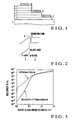
- Fig. 1 is a schematic sectional view showing an example of the arrangement of a heterostructure bipolar transistor according to an embodiment of the present invention.
- an n-type InP sub collector layer 2 heavily doped with silicon (Si)
- an InP collector layer 3 a p-type GaAs (0.51) Sb (0.49) base layer 4 heavily doped with carbon (C)
- an n-type InP cap layer 8 heavily doped with Si
- an n-type In (0.53) Ga( 0.47 )As contact layer 9 heavily doped with Si are stacked on an InP substrate 1 having a resistance increased by doping iron (Fe) as an impurity and having a (100) major surface.
- an ohmic-contact collector electrode 6 is formed on a region of the sub collector layer 2 where the collector layer 3 is not formed
- an ohmic-contact base electrode 5 is formed on a region of the base layer 4 where the emitter layer 7 is not formed
- an ohmic-contact emitter electrode 10 is formed on the contact layer 9.
- the sub-collector layer 2 is doped with, e.g., Si at 2 ⁇ 10 19 cm -3
- the base layer 4 is doped with, e.g., C at 1.1 ⁇ 10 20 cm -3
- the emitter layer 7 is doped with, e.g., Si at 5 ⁇ 10 17 cm -3
- the cap layer 8 is doped with, e.g., Si at 2 ⁇ 10 19 cm -3
- the contact layer 9 is doped with, e.g., Si at 3 ⁇ 10 19 cm -3 .
- the dopants and the constituent materials of the individual layers are not limited to those described above, and it is also possible to use other materials as long as a predetermined device operation can be realized.
- Sn can be applied as an n-type dopant instead of Si
- Zn or Be can be applied as a p-type dopant instead of C (carbon).
- a structure in which the compound semiconductor layers described above are sequentially formed (stacked) on the substrate 1 is obtained by the well-known crystal growth technique (apparatus) such as MBE (Molecular Beam Epitaxy) or MOCVD (Metal Organic Chemical Vapor Deposition). Then, a mesa structure as shown in Fig. 1 is formed by the well-known lithography technique and etching technique. A mask pattern having holes in electrode formation portions is then formed by lithography, and Ti/Pt/Au is deposited on this mask pattern. After that, the mask pattern is removed (lifted off) to form a base electrode 5, collector electrode 6, and emitter electrode 10.
- apparatus crystal growth technique
- MOCVD Metal Organic Chemical Vapor Deposition
- the emitter layer 7 is made of In (1-y) Al (y) P (y > 0). Therefore, as shown in a band diagram of Fig. 2 , in the conduction band edge, the emitter layer 7 has a higher potential than that of the base layer 4 at the interface between them. By contrast, in the band lineup near the emitter/base interface of the conventional InP/GaAsSb-based transistor, as shown in Fig. 16 , the potential in the conduction band edge on the side of an InP emitter is lower than that on the side of a GaAsSb base.
- this difference eliminates the barrier which exists near the emitter/base interface of the conventional device.
- electron accumulation near the emitter/base interface is suppressed, and this reduces the base-emitter capacitance.
- the difference between the conduction band on the side of the emitter layer 7 and the valance band on the side of the base layer 4 increases, so the tunneling recombination current at the emitter/base interface reduces.
- the current gain of the heterostructure bipolar transistor shown in Fig. 1 becomes larger than that of the conventional device.
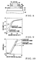
- Fig. 3 when compared to the dotted line indicating the conventional device in which the emitter is made of InP, the characteristic greatly improves as indicated by the solid line when the emitter layer is made of In (0.85) Al (0.15) P, although the Al content is low, 15%.
- Fig. 3 compares a base current I B , as a gummel-plot, of a heterostructure bipolar transistor using an emitter layer made of In (0.85) Al (0.15) P with that of a heterostructure bipolar transistor using an emitter layer made of InP.
- composition of InAlP forming the emitter layer and that of GaAsSb forming the base layer will be explained below.
- compositions by which the above-mentioned characteristics are obtained more effectively will be described from viewpoints indicated by (a), (b), (c), and (d) below.
- GaAs (x) Sb (1-x) formed on an InP substrate undergoes tensile strain when 0.51 ⁇ x ⁇ 1 and compression strain when 0 ⁇ x ⁇ 0.51 due to mismatching of the lattice constants.
- In (1-y) Al (y) P undergoes tensile strain as long as y > 0. It is generally impossible to make the film thickness of a strained layer larger than the critical film thickness. On the other hand, layers cannot be unlimitedly thinned for the reasons explained below.
- a doping concentration at which the crystal quality does not deteriorate is up to about 4 ⁇ 10 20 cm 3 in the case of carbon doping. Therefore, when the base resistance is decreased to increase the speed of a heterostructure bipolar transistor, e.g., when the base resistance is 600 ⁇ / ⁇ (cm 2 ), the film thickness is about 15 nm.
- the In (1-y) Al (y) P emitter layer when the In (1-y) Al (y) P emitter layer is thinned, its band bending becomes steep. Therefore, the conduction band of the In (1-y) Al (y) P layer approaches the valence band edge of the GaAsSb base layer and the emitter/base interface, and the increase in tunneling recombination current becomes significant. Accordingly, it is also impossible to unlimitedly thin the In (1-y) Al (y) P emitter layer.
- both the base layer made of GaAs (x) Sb (1-x) and the emitter layer made of In (1-y) Al (y) P must be so formed as to have a thickness which is equal to or smaller than the critical film thickness, and by which the device characteristics do not deteriorate. As conditions meeting this requirement, the ranges of the compositions x and y need only be 0.2 ⁇ x ⁇ 0.8 and 0 ⁇ y ⁇ 0.5, respectively.
- ⁇ Ec must be smaller than that in the case of GaAs (0.51) Sb (0.49 )/InP.
- the differences between the potential of the conduction band of InP and those of GaAS (x) Sb (1-x) and In (1-y) Al (y) can be estimated by the compositions x and y. Since ⁇ Ec of GaAs (0.51) Sb (0.49) /InP is estimated to be about 0.18 eV, the condition under which ⁇ Ec is 0.18 eV or less is 0.49x + 1.554y ⁇ 0.25 on the basis of the compositions x and y.
- Fig. 4 collectively shows the conditions derived from viewpoints (a), (b), (c), and (d) described above.
- a condition range indicated by a region 401 is a region where the effects of the present invention significantly appear.
- a region 402 is a region where the effects of the present invention are obtained.
- a region 403 is a region where the emitter/base conduction band edge discontinuity ( ⁇ Ec) becomes larger than that when the emitter is made of InP.
- a region 404 is a region where no device (heterostructure bipolar transistor) having a practical film thickness can be designed because the strain of the formed film is strong.
- the As content in the GaAsSb base layer may also be decreased away from the emitter layer side.
- the potential of the conduction band edge in the base layer lowers away from the emitter layer, and the internal electric field generated by this inclination accelerates the minority carriers in the base layer. This makes it possible to decrease the recombination probability of the minority carriers in the base layer, further increase the current gain, and also increase the operating speed of the device.
- FIG. 5A is a sectional view showing an example of the arrangement of the other heterostructure bipolar transistor according to the embodiment of the present invention
- Fig. 5B is a plan view. In this heterostructure bipolar transistor shown in Figs.
- Fe doping iron
- an ohmic-contact collector electrode 506 is formed on a region of the sub collector layer 502 where the collector layer 503 is not formed, an ohmic-contact base electrode 505 is formed on a region of the base layer 504 where the emitter layer 507 is not formed, and an ohmic-contact emitter electrode 510 is formed on the contact layer 509.
- the sub-collector layer 502 is doped with, e.g., Si at 2 ⁇ 10 19 cm -3
- the base layer 504 is doped with, e.g., C at 1.1 ⁇ 10 20 cm -3
- the emitter layer 507 is doped with, e.g., Si at 5 ⁇ 10 17 cm -3
- the cap layer 508 is doped with, e.g., Si at 2 ⁇ 10 19 cm -3
- the contact layer 509 is doped with, e.g., Si at 3 ⁇ 10 19 cm -3
- the film thicknesses of the collector layer 503, base layer 504, and emitter layer 507 are about 150, 20, and 30 nm, respectively.
- a structure in which the compound semiconductor layers described above are sequentially formed (stacked) on the substrate 501 is obtained by the well-known crystal growth technique (apparatus) such as MBE or MOCVD.
- apparatus crystal growth technique
- the substrate temperature during film formation is desirably 480°C or more in order to minimize the passivation of C acceptors by hydrogen.
- the substrate temperature may also be lower than the above-mentioned value if the passivation of C acceptors in the base layer 504 is suppressed, e.g., if the layers from the base layer 504 are to be formed by MBE after the layers up to the collector layer 503 are formed by MOCVD.
- a mesa structure as shown in Fig. 5A is formed by the well-known lithography technique and etching technique.
- an etching stopper layer or the like may also be used to obtain higher selectivity during the etching process, as long as the spirit and scope of the invention hold.
- a mask pattern having holes in electrode formation portions is then formed by lithography, and Ti/Pt/Au is deposited on this mask pattern. After that, the mask pattern is removed (lifted off) to form a base electrode 505, collector electrode 506, and emitter electrode 510.
- the stacked structures of these electrodes may also be made of other materials or may take different forms, provided that an ohmic contact with the underlying layer can be obtained in each electrode.
- the emitter layer 507 is made of InAlP. Therefore, as in the heterostructure bipolar transistor shown in Fig. 1 described above, in the conduction band edge, the emitter layer 507 has a higher potential than that of the base layer 504 at the interface between them. In the heterostructure bipolar transistor shown in Figs. 5A and 5B , this eliminates the barrier which exists near the emitter/base interface of the conventional device.
- the heterostructure bipolar transistor shown in Figs. 5A and 5B electron accumulation near the emitter/base interface is suppressed, and this reduces the base-emitter capacitance.
- the difference between the conduction band on the side of the emitter layer 507 and the valance band on the side of the base layer 504 increases, so the tunneling recombination current at the emitter/base interface decreases.
- the current gain increases in the heterostructure bipolar transistor shown in Figs. 5A and 5B as well when compared to that of the conventional device.
- Fig. 6 when compared to the dotted line indicating the conventional device in which the emitter is made of InP, the characteristic greatly improves as indicated by the solid line when the emitter layer is made of InAlP, although the Al content is decreased to 15%.
- Fig. 6 compares a base current I B , as a gummel-plot, of a heterostructure bipolar transistor using an emitter layer made of In (0.85) Al (0.15) P with that of a heterostructure bipolar transistor using an emitter layer made of InP.
- Fig. 7 shows the collector current I c - current grain characteristics.
- FIG. 8 is a sectional view showing an example of the arrangement of the heterostructure bipolar transistor according to the embodiment of the present invention. In this heterostructure bipolar transistor shown in Fig.
- the emitter layer 807 is in a graded composition state in which the In composition ratio changes from 0.75 to 1.00 and the Al composition ratio changes from 0.25 to 0, i.e., In increases and Al decreases, from the base layer 804 toward the cap layer 808.
- an ohmic-contact collector electrode 806 is formed on a region of the sub collector layer 802 where the collector layer 803 is not formed, an ohmic-contact base electrode 805 is formed on a region of the base layer 804 where the emitter layer 807 is not formed, and an ohmic-contact emitter electrode 810 is formed on the contact layer 809.
- the sub-collector layer 802 is doped with, e.g., Si at 2 ⁇ 10 19 cm -3
- the base layer 804 is doped with, e.g., C at 7 ⁇ 10 19 cm -3
- the emitter layer 807 is doped with, e.g., Si at 5 ⁇ 10 17 cm -3
- the cap layer 808 is doped with, e.g., Si at 1 ⁇ 10 19 cm -3
- the contact layer 809 is doped with, e.g., Si at 1.5 ⁇ 10 19 cm -3
- the film thicknesses of the collector layer 803, base layer 804, and emitter layer 807 are about 180, 20, and 30 nm, respectively.
- heterostructure bipolar transistor shown in Fig. 8 can be fabricated in the same manner as the heterostructure bipolar transistors shown in Fig. 1 and Figs. 5A and 5B described above.
- the emitter layer 807 is made of InAlP. Therefore, as in the heterostructure bipolar transistor shown in Fig. 1 described above, in the conduction band edge, the emitter layer 807 has a higher potential than that of the base layer 804 at the interface between them. In the heterostructure bipolar transistor shown in Fig. 8 , this eliminates the barrier which exists near the emitter/base interface of the conventional device.
- the heterostructure bipolar transistor shown in Fig. 8 As a consequence, in the heterostructure bipolar transistor shown in Fig. 8 , electron accumulation near the emitter/base interface is suppressed, and this reduces the base-emitter capacitance. At the same time, the difference between the conduction band on the side of the emitter layer 807 and the valance band on the side of the base layer 804 increases, so the tunneling recombination current at the emitter/base interface reduces. As a result of these effects, the current gain increases in the heterostructure bipolar transistor shown in Fig. 8 as well when compared to that of the conventional device.
- the emitter layer 807 has a graded composition, i.e., the Al composition ratio is high at the interface with the base layer 804 and lowers toward the cap layer 808. This alleviates the problem of strain caused by a high Al composition ratio.
- Fig. 9 when compared to the dotted line indicating the conventional device in which the emitter is made of InP, the characteristic greatly improves as indicated by the solid line when the emitter layer is made of InAlP having the graded composition as described above. Also, as is apparent from comparison with an emitter layer (an alternate long and two short dashed line) which has a similar graded composition and in which the composition is In (0.85 )Al (0.15) As at the interface with a base layer, as the Al composition ratio in the emitter layer in a region near the base layer rises, the recombination current component in a low-voltage region reduces. Note that Fig. 9 compares a base current I B , as a gummel-plot, of a heterostructure bipolar transistor using an emitter layer made of InAlP with that of a heterostructure bipolar transistor using an emitter layer made of InP.
- a base current I B as a gummel-plot
- the current gain characteristic improves as a whole and the characteristics of the heterostructure bipolar transistor greatly improve, when compared with the conventional device using InP as an emitter.
- the current gain is higher than that when the Al composition ratio in the emitter layer in the region near the base layer is low. This is probably because the high Al composition ratio adds the effect of discharging electrons from the emitter to the base.
- the emitter layer having the graded composition by which the Al composition ratio in the region near the base layer is high is used, a more notable current gain increasing effect can be obtained.
- FIG. 11 is a sectional view showing an example of the arrangement of the heterostructure bipolar transistor according to the embodiment of the present invention.
- this heterostructure bipolar transistor shown in Fig. 11 is a sectional view showing an example of the arrangement of the heterostructure bipolar transistor according to the embodiment of the present invention. In this heterostructure bipolar transistor shown in Fig.
- As contact layer 1110 heavily doped with Si are stacked on an InP substrate 1101 having a resistance increased by doping iron (Fe) as an impurity and having a (100) major surface.
- the collector compositionally-graded layer 1104 is in a graded composition state in which the In composition ratio changes from 1.00 to 0.92 and the Al composition ratio changes from 0 to 0.08, i.e., In reduces and Al increases, from collector layer 1103 toward the base layer 1105.
- the emitter layer 1108 is in a graded composition state in which the In composition ratio changes from 0.75 to 1.00 and the Al composition ratio changes from 0.25 to 0, i.e., In increases and Al reduces, from the base layer 1105 toward the cap layer 1109.
- an ohmic-contact collector electrode 1107 is formed on a region of the sub collector layer 1102 where the collector layer 1103 is not formed
- an ohmic-contact base electrode 1106 is formed on a region of the base layer 1105 where the emitter layer 1108 is not formed
- an ohmic-contact emitter electrode 1111 is formed on the contact layer 1110.
- the sub-collector layer 1102 is doped with, e.g., Si at 2 ⁇ 10 19 cm -3
- the base layer 1105 is doped with, e.g., C at 7 ⁇ 10 19 cm -3
- the emitter layer 1108 is doped with, e.g., Si at 5 ⁇ 10 17 cm -3
- the cap layer 1109 is doped with, e.g., Si at 1 ⁇ 10 19 cm -3
- the contact layer 1110 is doped with, e.g., Si at 1.5 ⁇ 10 19 cm -3
- the film thicknesses of the collector layer 1103, collector compositionally-graded layer 1104, base layer 1105, and emitter layer 1108 are about 1110, 30, 20, and 30 nm, respectively.
- heterostructure bipolar transistor shown in Fig. 11 can be fabricated in the same manner as the heterostructure bipolar transistors shown in Fig. 1 , Figs. 5A and 5B , and Fig. 8 described above.
- the emitter layer 1108 is made of InAlP. Therefore, as in the heterostructure bipolar transistors shown in Figs. 1 , 5A , and 8 described above, in the conduction band edge, the emitter layer 1108 has a higher potential than that of the base layer 1105 at the interface between them. In the heterostructure bipolar transistor shown in Fig. 8 , this eliminates the barrier which exists near the emitter/base interface of the conventional device.
- the heterostructure bipolar transistor shown in Fig. 11 As a consequence, in the heterostructure bipolar transistor shown in Fig. 11 , electron accumulation near the emitter/base interface is suppressed, and this reduces the base-emitter capacitance. At the same time, the difference between the conduction band on the side of the emitter layer 1108 and the valance band on the side of the base layer 1105 increases, so the tunneling recombination current at the emitter/base interface reduces. As a result of these effects, the current gain increases in the heterostructure bipolar transistor shown in Fig. 11 as well when compared to that of the conventional device.
- the emitter layer 1108 has a graded composition, i.e., the Al composition ratio is high at the interface with the base layer 1105 and lowers toward the cap layer 1109. This alleviates the problem of strain caused by a high Al composition ratio, so a higher current gain is obtained as in the heterostructure bipolar transistor shown in Fig. 8 .
- the composition of the collector in a region in contact with the base 1105 is InAlP. This makes it possible to solve the problem of a boundary layer at the collector/base interface to be explained below.
- the melting points of compound semiconductors containing Sb are lower than those of compound semiconductors made only of P and As as other group-V atoms.
- Examples of compound semiconductors made of two devices are GaSb (712°C) and InSb (524°C) against GaP (1,467°C), InP (1,060°C), GaAs (1,240°C), and InAs (942°C).
- a general growth temperature range of GaAsSb is 500°C to 600°C.
- this layer generates transition defects by locally producing a strong strain, and locally increases or decreases the potential in the conduction band edge or valence band edge near the interface. For example, if a boundary layer mainly containing InSb forms at the GaAsSb/InP interface, a local drop occurs in the conduction band edge as shown in Fig. 12 . Consequently, the recombination current increases via the defects to lower the current gain, and the drop or rise in the conduction band edge interferes with collector-to-base electron traveling, thereby deteriorating the device characteristics, e.g., decreasing the operating speed of the device.
- GaAsSb base layer lower than the melting point of InSb, thereby preventing the interface from changing into a liquid phase even when In-Sb bonds form on the contact surface between the collector layer made of InP and the base layer (GaAsSb).
- the heterostructure bipolar transistor shown in Fig. 11 includes the InAlP collector compositionally-graded layer 1104 in a region where the base layer 1105 is to be formed, so that the base layer 1105 is formed on this InAIP layer.
- the formation of the boundary layer made of In and Sb can be suppressed. The suppression of the boundary layer will be explained in more detail below.
- compound semiconductors containing Sb have low melting points
- compound semiconductors containing Al have high melting points.
- Examples are AlP (which sublimates at about 1,060°C), AlAs (1,740°C), and AlSb (1,080°C).
- the bonding energy of atoms increases in the order of Al-Sb > Ga-Sb > In-Sb, and is most stable in Al-Sb. Therefore, Al-Sb bonds form in preference to In-Sb bonds at the interface when a compound semiconductor containing aluminum is inserted at the interface between the collector layer and base layer, or when the collector layer is made of In (1-z) Al (z) P (z > 0).
- GaAs (x) Sb (1-x) formed on an InP substrate undergoes tensile strain when 0.51 ⁇ x ⁇ 1 and compression strain when 0 ⁇ x ⁇ 0.51 due to mismatching of the lattice constants.
- In (1-z) Al (z) P undergoes tensile strain as long as z > 0. It is generally impossible to make the film thickness of a strained layer larger than the critical film thickness. On the other hand, layers cannot be unlimitedly thinned for the reasons explained below.
- a doping concentration at which the crystal quality does not deteriorate is up to about 4 ⁇ 10 20 cm 3 in the case of carbon doping. Therefore, when the base resistance is to be decreased to increase the speed of a heterostructure bipolar transistor, a film thickness of about 15 nm is necessary for, e.g., a base resistance of 600 ⁇ / ⁇ (cm 2 ) and a doping concentration of 4 ⁇ 10 20 cm 3 , and a film thickness of about 35 nm is necessary for a doping concentration of 8 ⁇ 10 19 cm 3 .
- a film having a film thickness which is equal to or smaller than the critical film thickness and does not deteriorate the device characteristics must be formed for both GaAs (x) Sb (1-x) and In (1-z) Al (z) P.
- a practical range of x viewed from the critical film thickness is 0.2 ⁇ x ⁇ 0.8 which takes account of the base resistance and the process margin resulting from fluctuation of the film thickness, and by which no criticality is reached even with a film thickness of 15 nm.
- the problems of the boundary layer can be eliminated if the base layer is made of GaAs (z) Sb (1-x) , the interface on the collector layer side of the base layer is made of In (1-z) Al (z) P, the ranges of the compositions x and z are 0.40 ⁇ x ⁇ 0.55 and 0 ⁇ z ⁇ 0.18, respectively, and the relationship between x and z is 0.49x + 1.554z ⁇ 0.36.
- the composition of the base/collector interface steeply changes because the collector compositionally-graded layer 1104 is formed. Consequently, as shown in a band diagram of Fig. 13 , the local drop in the conduction band edge near the base/collector interface is suppressed, so a state in which there is no obstacle to the transit of electrons can be realized.
- the boundary layer described previously is formed at the interface. This may interfere with selective etching from the base layer to the collector layer when wet chemical etching for forming the structure as shown in Fig. 11 is performed. If the boundary layer exists at the base/collector interface, the etching behavior changes near the interface regardless of whether the etchant is for the base or collector, and this makes the designed structure difficult to realize.
- the present invention described above can provide a heterostructure bipolar transistor capable of high-speed operation.
Landscapes
- Bipolar Transistors (AREA)
- Electrodes Of Semiconductors (AREA)
Abstract
Claims (14)
- Transistor bipolaire à hétérostructure, caractérisé en ce que des dispositifs constituants d'un semi-conducteur composite formant une couche de base contiennent au moins du Ga, de l'As et du Sb, et des dispositifs constituants d'un semi-conducteur composite formant une couche d'émetteur contiennent au moins du In, de l'Al et du P.
- Transistor bipolaire à hétérostructure selon la revendication 1, caractérisé en ce qu'il comprend :un substrat réalisé à partir d'InP ;une couche de collecteur formée sur ledit substrat et réalisée à partir d'un semi-conducteur composite contenant de l'indium et du phosphore ;ladite couche de base formée sur ladite couche de collecteur et réalisée à partir d'un semi-conducteur composite de type p contenant du gallium, de l'arsenic et de l'antimoine ; etladite couche d'émetteur formée sur ladite couche de base et réalisée à partir d'un semi-conducteur composite de type n contenant de l'indium, de l'aluminium et du phosphore,dans lequel un rapport de composition d'indium sur aluminium dans ladite couche d'émetteur est dans la gamme dans laquelle une énergie potentielle, dans une bande de conduction sur un côté de ladite couche de base, de ladite couche d'émetteur n'est pas inférieure à celle dans une bande de conduction de ladite couche de base.
- Transistor bipolaire à hétérostructure selon la revendication 1, caractérisé en ce que au moins une couche de GaAs(x)Sb(1-x) est utilisée dans ladite couche de base, au moins une couche de In(1-y)Al(y)P est utilisée dans ladite couche d'émetteur, et x et y représentent des compositions cristallines mixtes et sont dans des gammes de 0 < x < 1 et 0 < y < 1, respectivement.
- Transistor bipolaire à hétérostructure selon la revendication 3, caractérisé en ce que la gamme de la composition x est 0,2 ≤ x ≤ 0,8, et la gamme de la composition y est 0 ≤ y ≤ 0,5.
- Transistor bipolaire à hétérostructure selon la revendication 4, caractérisé en ce qu'une relation entre x et y est 0,49x + 1,554y ≥ 0,25.
- Transistor bipolaire à hétérostructure selon la revendication 5, caractérisé en ce que les gammes des compositions x et y sont 0,45 ≤ x ≤ 0,55 et 0 ≤ y ≤ 0,25, respectivement, et la relation entre x et y est 0,49x + 1,554y ≥ 0,36.
- Transistor bipolaire à hétérostructure selon la revendication 1, caractérisé en ce que le rapport de composition de Al dans ladite couche d'émetteur diminue à mesure que l'on s'éloigne de ladite couche de base.
- Transistor bipolaire à hétérostructure selon la revendication 1, caractérisé en ce que le rapport de composition de As dans ladite couche de base diminue à mesure que l'on s'éloigne de ladite couche d'émetteur.
- Transistor bipolaire hétérorestructure selon la revendication 1, caractérisé en ce que la couche de collecteur est fabriquée à partir d'un semi-conducteur composite contenant de l'indium, de l'aluminium, et du phosphore.
- Transistor bipolaire à hétérostructure selon la revendication 1, caractérisé en ce que
ladite couche de base est fabriquée à partir de GaAs(x)Sb(1-x),
ladite couche de collecteur est fabriquée à partir de In(1-z)Al(z)P, et
x et y représentent des compositions cristallines mixtes et sont dans la gamme de 0 < x < 1 et 0 < z < 1, respectivement. - Transistor bipolaire à hétérostructure selon la revendication 10, caractérisé en ce que
la gamme de la composition z est 0 < z ≤ 0,18, et
la relation entre x et z est 0,49x + 1,554z ≥ 0,36. - Transistor bipolaire à hétérostructure selon la revendication 9, caractérisé en ce que le rapport de composition de Al dans ladite couche de collecteur diminué à mesure que l'on s'éloigne de ladite couche de base.
- Transistor bipolaire à hétérostructure selon la revendication 1, caractérisé en ce que
des couches incluant ladite couche de base et ladite couche d'émetteur formant le transistor bipolaire à hétérostructure sont formées par dépôt de vapeur chimique organique métallique, et
du carbone est introduit comme dopant dans ladite couche de base. - Transistor bipolaire à hétérostructure selon la revendication 13, caractérisé en ce que ladite couche de base est formée à une température de croissance qui n'est pas inférieure à 480°C.
Applications Claiming Priority (3)
| Application Number | Priority Date | Filing Date | Title |
|---|---|---|---|
| JP2004195533 | 2004-07-01 | ||
| JP2004265753 | 2004-09-13 | ||
| PCT/JP2005/011606 WO2006003845A1 (fr) | 2004-07-01 | 2005-06-24 | Transistor bipolaire à hétérojonction |
Publications (3)
| Publication Number | Publication Date |
|---|---|
| EP1662557A1 EP1662557A1 (fr) | 2006-05-31 |
| EP1662557A4 EP1662557A4 (fr) | 2009-04-08 |
| EP1662557B1 true EP1662557B1 (fr) | 2011-08-17 |
Family
ID=35782656
Family Applications (1)
| Application Number | Title | Priority Date | Filing Date |
|---|---|---|---|
| EP05765094A Expired - Lifetime EP1662557B1 (fr) | 2004-07-01 | 2005-06-24 | Transistor bipolaire à hétérojonction |
Country Status (5)
| Country | Link |
|---|---|
| US (1) | US7242038B2 (fr) |
| EP (1) | EP1662557B1 (fr) |
| JP (1) | JP4575378B2 (fr) |
| CA (1) | CA2529595C (fr) |
| WO (1) | WO2006003845A1 (fr) |
Families Citing this family (9)
| Publication number | Priority date | Publication date | Assignee | Title |
|---|---|---|---|---|
| JP4799938B2 (ja) * | 2005-07-14 | 2011-10-26 | 日本電信電話株式会社 | ヘテロ接合バイポーラトランジスタ |
| GB2447921B (en) * | 2007-03-28 | 2012-01-25 | Rfmd Uk Ltd | A Transistor |
| US8395237B2 (en) * | 2008-10-21 | 2013-03-12 | Nec Corporation | Group nitride bipolar transistor |
| JP5628681B2 (ja) | 2008-10-21 | 2014-11-19 | ルネサスエレクトロニクス株式会社 | バイポーラトランジスタ |
| JP5681031B2 (ja) * | 2011-04-18 | 2015-03-04 | 日本電信電話株式会社 | ヘテロ接合バイポーラトランジスタ |
| WO2013058640A2 (fr) * | 2011-10-20 | 2013-04-25 | Zepeda Lopez Hector Manuel | Procédé d'extraction, d'essai et de comptage d'extrait dialysé de leucocytes provenant de rate de requin, pour obtenir un facteur de transfert potentialisé, spécifiquement conçu pour être utilisé en tant que traitement contre la maladie connue sous le nom d'asthme |
| US9847407B2 (en) | 2011-11-16 | 2017-12-19 | Skyworks Solutions, Inc. | Devices and methods related to a gallium arsenide Schottky diode having low turn-on voltage |
| US9461153B2 (en) * | 2011-11-16 | 2016-10-04 | Skyworks Solutions, Inc. | Devices and methods related to a barrier for metallization of a gallium based semiconductor |
| TWI505409B (zh) * | 2012-06-13 | 2015-10-21 | Win Semiconductors Corp | 一種化合物半導體晶圓結構 |
Family Cites Families (11)
| Publication number | Priority date | Publication date | Assignee | Title |
|---|---|---|---|---|
| US4794440A (en) * | 1983-05-25 | 1988-12-27 | American Telephone And Telegraph Company, At&T Bell Laboratories | Heterojunction bipolar transistor |
| US4821082A (en) * | 1987-10-30 | 1989-04-11 | International Business Machines Corporation | Heterojunction bipolar transistor with substantially aligned energy levels |
| JPH06310521A (ja) * | 1993-04-23 | 1994-11-04 | Nippon Telegr & Teleph Corp <Ntt> | バイポーラトランジスタ |
| JPH11121461A (ja) * | 1997-10-08 | 1999-04-30 | Fujitsu Ltd | ヘテロ接合バイポーラトランジスタ |
| US6696710B2 (en) | 2001-02-27 | 2004-02-24 | Agilent Technologies, Inc. | Heterojunction bipolar transistor (HBT) having an improved emitter-base junction |
| US6762480B2 (en) | 2001-02-27 | 2004-07-13 | Agilent Technologies, Inc. | Thin gallium-arsenide-antimonide base heterojunction bipolar transistor (HBT) having improved gain |
| JP2003086602A (ja) * | 2001-09-14 | 2003-03-20 | Nippon Telegr & Teleph Corp <Ntt> | ヘテロ接合バイポーラトランジスタ |
| JP2003297849A (ja) * | 2002-04-05 | 2003-10-17 | Toshiba Corp | ヘテロ接合バイポーラトランジスタ及びその製造方法 |
| JP2004214576A (ja) * | 2003-01-09 | 2004-07-29 | Nippon Telegr & Teleph Corp <Ntt> | ヘテロバイポーラトランジスタ |
| US6822274B2 (en) * | 2003-02-03 | 2004-11-23 | Agilent Technologies, Inc. | Heterojunction semiconductor device having an intermediate layer for providing an improved junction |
| JP2005086135A (ja) * | 2003-09-11 | 2005-03-31 | Nippon Telegr & Teleph Corp <Ntt> | ヘテロバイポーラトランジスタ用エピタキシャルウエハおよびその製造方法 |
-
2005
- 2005-06-24 CA CA2529595A patent/CA2529595C/fr not_active Expired - Fee Related
- 2005-06-24 JP JP2006523763A patent/JP4575378B2/ja not_active Expired - Fee Related
- 2005-06-24 WO PCT/JP2005/011606 patent/WO2006003845A1/fr not_active Ceased
- 2005-06-24 US US10/560,756 patent/US7242038B2/en not_active Expired - Fee Related
- 2005-06-24 EP EP05765094A patent/EP1662557B1/fr not_active Expired - Lifetime
Also Published As
| Publication number | Publication date |
|---|---|
| WO2006003845A1 (fr) | 2006-01-12 |
| EP1662557A1 (fr) | 2006-05-31 |
| CA2529595A1 (fr) | 2006-01-01 |
| JPWO2006003845A1 (ja) | 2008-04-10 |
| US7242038B2 (en) | 2007-07-10 |
| US20060231859A1 (en) | 2006-10-19 |
| CA2529595C (fr) | 2013-02-26 |
| EP1662557A4 (fr) | 2009-04-08 |
| JP4575378B2 (ja) | 2010-11-04 |
Similar Documents
| Publication | Publication Date | Title |
|---|---|---|
| EP0445475B1 (fr) | Transistor bipolaire à hétérojonction | |
| US5903018A (en) | Bipolar transistor including a compound semiconductor | |
| US20020070390A1 (en) | Superlattice fabrication for InAs/GaSb/AISb semiconductor structures | |
| EP0619613B1 (fr) | Transisitor bipolaire à hétérojonction | |
| TWI695504B (zh) | 異質接面雙極性電晶體 | |
| US20030032253A1 (en) | InPSb/InAs BJT device and method of making | |
| JPH038340A (ja) | ヘテロ接合バイポーラトランジスタ | |
| US20060267007A1 (en) | Devices incorporating heavily defected semiconductor layers | |
| US7821037B2 (en) | Heterojunction bipolar transistor | |
| EP1662557B1 (fr) | Transistor bipolaire à hétérojonction | |
| US8441037B2 (en) | Semiconductor device having a thin film stacked structure | |
| US5571732A (en) | Method for fabricating a bipolar transistor | |
| US20070018192A1 (en) | Devices incorporating heavily defected semiconductor layers | |
| US6768141B2 (en) | Heterojunction bipolar transistor (HBT) having improved emitter-base grading structure | |
| CN100521234C (zh) | 异质结半导体器件及其制造方法 | |
| Hoshi et al. | InGaP/GaAsSb/InGaAsSb double heterojunction bipolar transistors with 703-GHz fmax and 5.4-V breakdown voltage | |
| CN100463121C (zh) | 异质结构双极型晶体管 | |
| JP4799938B2 (ja) | ヘテロ接合バイポーラトランジスタ | |
| Fang et al. | $ W_ {e}= 100\mathrm {nm} $ InP/lnGaAs DHBT with Self-aligned MOCVD Regrown p-GaAs Extrinsic Base Exhibiting $1\Omega-\mu\mathrm {m}^{2} $ Base Contact Resistivity | |
| CN115188805B (en) | Heterojunction bipolar transistor | |
| Ohkubo et al. | High-reliability InGaP/GaAs HBTs with 153 GHz f T and 170 GHz f max | |
| WO2025262958A1 (fr) | Transistor bipolaire à hétérojonction | |
| JP2002076015A (ja) | ヘテロ接合型バイポーラトランジスタ | |
| US20080230803A1 (en) | Integrated Contact Interface Layer | |
| Ohkubo et al. | High-reliability InGaP/GaAs HBTs with 153 GHz f^ sub T^ and 170 GHz f^ sub max^ |
Legal Events
| Date | Code | Title | Description |
|---|---|---|---|
| PUAI | Public reference made under article 153(3) epc to a published international application that has entered the european phase |
Free format text: ORIGINAL CODE: 0009012 |
|
| 17P | Request for examination filed |
Effective date: 20051220 |
|
| AK | Designated contracting states |
Kind code of ref document: A1 Designated state(s): AT BE BG CH CY CZ DE DK EE ES FI FR GB GR HU IE IS IT LI LT LU MC NL PL PT RO SE SI SK TR |
|
| AX | Request for extension of the european patent |
Extension state: AL BA HR LV MK YU |
|
| RBV | Designated contracting states (corrected) |
Designated state(s): DE FR GB |
|
| DAX | Request for extension of the european patent (deleted) | ||
| RBV | Designated contracting states (corrected) |
Designated state(s): DE FR GB |
|
| A4 | Supplementary search report drawn up and despatched |
Effective date: 20090310 |
|
| GRAP | Despatch of communication of intention to grant a patent |
Free format text: ORIGINAL CODE: EPIDOSNIGR1 |
|
| GRAS | Grant fee paid |
Free format text: ORIGINAL CODE: EPIDOSNIGR3 |
|
| GRAA | (expected) grant |
Free format text: ORIGINAL CODE: 0009210 |
|
| AK | Designated contracting states |
Kind code of ref document: B1 Designated state(s): DE FR GB |
|
| REG | Reference to a national code |
Ref country code: GB Ref legal event code: FG4D |
|
| REG | Reference to a national code |
Ref country code: DE Ref legal event code: R096 Ref document number: 602005029582 Country of ref document: DE Effective date: 20111020 |
|
| PLBE | No opposition filed within time limit |
Free format text: ORIGINAL CODE: 0009261 |
|
| STAA | Information on the status of an ep patent application or granted ep patent |
Free format text: STATUS: NO OPPOSITION FILED WITHIN TIME LIMIT |
|
| 26N | No opposition filed |
Effective date: 20120521 |
|
| REG | Reference to a national code |
Ref country code: DE Ref legal event code: R097 Ref document number: 602005029582 Country of ref document: DE Effective date: 20120521 |
|
| REG | Reference to a national code |
Ref country code: FR Ref legal event code: PLFP Year of fee payment: 12 |
|
| REG | Reference to a national code |
Ref country code: FR Ref legal event code: PLFP Year of fee payment: 13 |
|
| PGFP | Annual fee paid to national office [announced via postgrant information from national office to epo] |
Ref country code: GB Payment date: 20170620 Year of fee payment: 13 Ref country code: DE Payment date: 20170621 Year of fee payment: 13 Ref country code: FR Payment date: 20170621 Year of fee payment: 13 |
|
| REG | Reference to a national code |
Ref country code: DE Ref legal event code: R119 Ref document number: 602005029582 Country of ref document: DE |
|
| GBPC | Gb: european patent ceased through non-payment of renewal fee |
Effective date: 20180624 |
|
| PG25 | Lapsed in a contracting state [announced via postgrant information from national office to epo] |
Ref country code: FR Free format text: LAPSE BECAUSE OF NON-PAYMENT OF DUE FEES Effective date: 20180630 Ref country code: DE Free format text: LAPSE BECAUSE OF NON-PAYMENT OF DUE FEES Effective date: 20190101 Ref country code: GB Free format text: LAPSE BECAUSE OF NON-PAYMENT OF DUE FEES Effective date: 20180624 |