EP1662660A2 - Verfahren und Gerät zum Kompensieren gegen Temperatur-, Spannungs- und Herstellungsschwankungen - Google Patents
Verfahren und Gerät zum Kompensieren gegen Temperatur-, Spannungs- und Herstellungsschwankungen Download PDFInfo
- Publication number
- EP1662660A2 EP1662660A2 EP05025953A EP05025953A EP1662660A2 EP 1662660 A2 EP1662660 A2 EP 1662660A2 EP 05025953 A EP05025953 A EP 05025953A EP 05025953 A EP05025953 A EP 05025953A EP 1662660 A2 EP1662660 A2 EP 1662660A2
- Authority
- EP
- European Patent Office
- Prior art keywords
- circuit
- transistors
- pmos
- bulk
- nmos
- Prior art date
- Legal status (The legal status is an assumption and is not a legal conclusion. Google has not performed a legal analysis and makes no representation as to the accuracy of the status listed.)
- Ceased
Links
- 238000000034 method Methods 0.000 title claims abstract description 83
- 230000008569 process Effects 0.000 title claims abstract description 66
- 238000001514 detection method Methods 0.000 claims abstract description 29
- 239000000758 substrate Substances 0.000 claims description 20
- 230000007423 decrease Effects 0.000 claims description 19
- 230000000694 effects Effects 0.000 claims description 15
- 239000004065 semiconductor Substances 0.000 claims description 14
- 230000001965 increasing effect Effects 0.000 claims description 7
- 230000008859 change Effects 0.000 abstract description 10
- 230000007704 transition Effects 0.000 description 15
- 230000001276 controlling effect Effects 0.000 description 8
- 238000010586 diagram Methods 0.000 description 6
- 230000001419 dependent effect Effects 0.000 description 4
- 230000007613 environmental effect Effects 0.000 description 4
- 238000005513 bias potential Methods 0.000 description 3
- 230000005540 biological transmission Effects 0.000 description 3
- 230000006872 improvement Effects 0.000 description 3
- 238000004088 simulation Methods 0.000 description 3
- 238000004519 manufacturing process Methods 0.000 description 2
- 230000003071 parasitic effect Effects 0.000 description 2
- FDORQEIHOKEJNX-UHFFFAOYSA-N 2-[[3-(4-fluorophenyl)-3-(4-phenylphenoxy)propyl]-methylamino]acetic acid Chemical compound C=1C=C(F)C=CC=1C(CCN(C)CC(O)=O)OC(C=C1)=CC=C1C1=CC=CC=C1 FDORQEIHOKEJNX-UHFFFAOYSA-N 0.000 description 1
- 101150070189 CIN3 gene Proteins 0.000 description 1
- RYGMFSIKBFXOCR-UHFFFAOYSA-N Copper Chemical compound [Cu] RYGMFSIKBFXOCR-UHFFFAOYSA-N 0.000 description 1
- 101100508840 Daucus carota INV3 gene Proteins 0.000 description 1
- 241001506308 Potato virus T Species 0.000 description 1
- 230000003044 adaptive effect Effects 0.000 description 1
- 230000015556 catabolic process Effects 0.000 description 1
- 229910052802 copper Inorganic materials 0.000 description 1
- 239000010949 copper Substances 0.000 description 1
- 230000002596 correlated effect Effects 0.000 description 1
- 230000000875 corresponding effect Effects 0.000 description 1
- 230000003247 decreasing effect Effects 0.000 description 1
- 238000006731 degradation reaction Methods 0.000 description 1
- 230000002708 enhancing effect Effects 0.000 description 1
- 230000007246 mechanism Effects 0.000 description 1
- 238000006386 neutralization reaction Methods 0.000 description 1
- 229920002102 polyvinyl toluene Polymers 0.000 description 1
- 230000009467 reduction Effects 0.000 description 1
Images






Classifications
-
- H—ELECTRICITY
- H03—ELECTRONIC CIRCUITRY
- H03K—PULSE TECHNIQUE
- H03K3/00—Circuits for generating electric pulses; Monostable, bistable or multistable circuits
- H03K3/01—Details
- H03K3/011—Modifications of generator to compensate for variations in physical values, e.g. voltage, temperature
-
- H—ELECTRICITY
- H03—ELECTRONIC CIRCUITRY
- H03K—PULSE TECHNIQUE
- H03K17/00—Electronic switching or gating, i.e. not by contact-making and –breaking
- H03K17/14—Modifications for compensating variations of physical values, e.g. of temperature
- H03K17/145—Modifications for compensating variations of physical values, e.g. of temperature in field-effect transistor switches
-
- H—ELECTRICITY
- H03—ELECTRONIC CIRCUITRY
- H03K—PULSE TECHNIQUE
- H03K19/00—Logic circuits, i.e. having at least two inputs acting on one output; Inverting circuits
- H03K19/003—Modifications for increasing the reliability for protection
- H03K19/00369—Modifications for compensating variations of temperature, supply voltage or other physical parameters
- H03K19/00384—Modifications for compensating variations of temperature, supply voltage or other physical parameters in field effect transistor circuits
-
- H—ELECTRICITY
- H03—ELECTRONIC CIRCUITRY
- H03K—PULSE TECHNIQUE
- H03K3/00—Circuits for generating electric pulses; Monostable, bistable or multistable circuits
- H03K3/02—Generators characterised by the type of circuit or by the means used for producing pulses
- H03K3/353—Generators characterised by the type of circuit or by the means used for producing pulses by the use, as active elements, of field-effect transistors with internal or external positive feedback
- H03K3/356—Bistable circuits
- H03K3/3565—Bistables with hysteresis, e.g. Schmitt trigger
Definitions
- the present invention relates to a method and apparatus for providing compensation against temperature, process and supply voltage variation.
- the transmitted signal gets worst when the ground and supply references bounce (because of pin package inductance, for instance) thus making logic high and low levels equal to damped sinusoidal signals.
- a Schmitt trigger circuit is frequently used at the receiver end to filter the noise.
- a Schmitt trigger is an electronic circuit used to turn a signal having slow or asymmetrical transition into a signal with a sharp transition region. Such a Schmitt trigger circuit cleans up the input signal from noise and provides very sharp transitions.
- Schmitt trigger circuits are slower and consume more power compared to similar non-Schmitt circuits.
- the Schmitt circuit characteristic is very much dependent on process and temperature variations because process and temperature directly affects the threshold voltages, which is not under control.
- Schmitt trigger circuit For very slow transitions and long distance transmissions, a Schmitt trigger circuit with large value of hysteresis is thus required.
- FIG 1 diagrammatically shows a semiconductor integrated circuit incorporated with substrate bias control circuit, realised according to the prior art and described in the USPN 5461338.
- Bias potential generation circuits 5 and 6 generate bias voltage only if the circuit is in normal mode (not in standby mode).
- bias generation circuits 5 and 6 generate two separate signals for the well of PMOS transistors and the substrate of NMOS transistors which forward biases the body-source of the CMOS configurations. It helps in reduction of the threshold voltages of the CMOS configurations and hence better speed is achieved.
- bias potential must be smaller than the flat band voltage between semiconductor substrate and source junction of the transistors. This bias potential is not generated in standby mode to reduce power.
- switching circuits 2 and 3 have been introduced between the body and the source junctions of the transistors to take care of the standby signal.
- a separate standby detection circuit 4 generates the standby signal.
- the proposed architecture saves power in standby mode and achieves significant improvement in the operational speed especially when a high voltage device is operated at low voltages.
- the proposed integrated circuit does not take care of the process, temperature or supply voltage variations. So it is very sensitive to the process and environmental conditions and tt may lead to more power consumption if bias voltage becomes greater than the flat-band voltage.
- FIG. 2 diagrammatically shows another prior art control device aimed to enhance the operational speed even at very low supply voltages, as described in USPN 6515534.
- the illustrated diodes D1 and D2 are the parasitic diodes formed between body and source/drain junction of a PMOS transistor 21.
- INV3 and INV4 are two CMOS inverters, which detect a gate signal of the PMOS transistor 21 and generate a bias signal for the body of the PMOS transistor 21.
- the body (well) of the PMOS transistor 21 also goes low and diodes D 1 and D2 are forward biased. This reduces the threshold voltage of the PMOS transistor 21 and provides more drain current through diodes D1 and D2, which increase the operational speed of the PMOS transistor 21.
- the described circuit detects the signal from the gate of the MOS transistor or device and biases the body accordingly so that the device operates in a faster manner.
- Schmitt trigger circuits As already described, also known in the field of the invention are Schmitt trigger circuits.
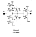
- FIG. 3 schematically shows a widely used conventional Schmitt trigger circuit.
- Such a circuit comprises four stacked parallel input MOSFET transistors P1, P2, N1 and N2 which are coupled by their respective gate electrodes to a trigger input terminal IN of the trigger circuit.
- VP or VN signals are generated by the input transistors, such signals being controlled by the transistor size ratios P3/P1 and N3/N1.
- MOS transistors M1 and M2 make an output inverter to provide a sharp transition at an output terminal OUT of the trigger circuit.
- the known Schmitt trigger circuit also comprises further MOS transistors, P3 and N3, which realise a feedback structure to control the input PMOS and NMOS transistors.
- the transistor P3 is OFF and the transistor N3 is ON and thus the signal at the output terminal OUT goes low.
- the transistor NMOS N1 begins to turn ON and the signal VN starts to fall down.
- a first or low-to-high trip point (Vih) of this Schmitt trigger circuit is defined when the signal at the trigger input terminal IN is equal to Vtn2+VN, therein Vtn2 is the threshold voltage of the NMOS transistor N2, such a condition corresponding to when the NMOS transistor N2 turns ON.
- the N2 transistor size is large when compared to the sizes of the transistors N1 and N3, then the low-to-high trip point (Vih) is accurately decided by the ratio of N3/N1. Similarly, a high-to-low trip point (Vil) is decided by the ratio of P3/P1.
- This known circuit is sensitive to the positive supply voltage VDDS as well as to the process because the threshold voltage Vth of the transistors P3 and N3 keeps on changing as the node VP or VN goes up or comes down respectively with the signal at the trigger input terminal IN. In summary, at low supply voltage this known circuit does not work properly.
- Another object of the invention is to an apparatus for providing compensation against temperature, process and supply voltage variation as claimed in claims 6 for a MOS circuit and in claim 9 for a CMOS circuit.
- Yet another object of the invention is a compensated circuit against temperature, process and supply voltage variation as claimed in claim 15.
- the present invention provides structures and methods for a very stable MOS circuit.
- the high and low threshold levels of the proposed circuit are very less sensitive to process, temperature and voltage, which provides stable hysteresis.
- Different implementations of the method have been presented for low power, high speed and minimum area.
- the method for providing compensation against temperature, process and supply voltage variation according to the present invention can be used to control any type of CMOS circuits.
- a block diagram showing the principles of the proposed method is shown in Figure 4.
- Figure 4 shows in a block diagram the detection of the change in process, temperature and supply voltage (also referred to as PVT - process, voltage, temperature variation) and its application in controlling a device characteristic and behavior, the device being generally indicated by 90.
- PVT - process also referred to as PVT - process, voltage, temperature variation
- a PVT detection circuit 100 includes bulk control circuits 91 & 95 and drive control circuits 92 & 96 to generate control signals for the substrates of the PMOS and NMOS transistors included in the device to be controlled and for driving respective PMOS and NMOS drive control circuits 93 & 94.
- the drive control circuits 92 & 96 are connected to the respective PMOS and NMOS drive control circuits, 93 and 94, which control the drive level of the MOS transistors included in the device to be controlled, in particular a CMOS device including PMOS and NMOS transistors.
- the bulk control circuit 91 is connected to a Nwell portion of a PMOS circuit block of the device 90 and the bulk control circuit 95 is connected to a substrate portion of a NMOS circuit block of the device 90, while the PMOS drive control circuit 93 is connected to a PMOS drive logic of the device 90 and the NMOS drive control circuit 94 is connected to a NMOS drive logic of the device 90.
- the drive control circuit 92 is connected to the PMOS drive control circuit 93 and the drive control circuit 96 is connected to the NMOS drive control circuit 94.
- the proposed PVT detection circuit 100 does not take any input or control signal from the device internal elements and it is completely independent of the modes of operation of the devices to be controlled. Moreover, the PVT detection circuit 100 can be different for the body-bias control or the drive control, being thus flexible for different possibility of implementation.
- the PVT detection circuit 100 separately generates four control signals namely control signals for Nwell (body of the PMOS transistors), substrate (body of the NMOS transistors) and two other signals for the PMOS and NMOS drive control circuits 93 & 94, which can be implemented in several ways.
- control signals assist in controlling the bulk voltage and drive level in a MOS circuit. Accordingly a stable threshold voltage is maintained in the transistors included in the device 90 to be controlled by providing compensation against temperature, process and supply voltage variation.
- the method for providing compensation against temperature, process and supply voltage variation in a device comprising MOS transistors advantageously comprises the steps of:
- the step of controlling the bulk bias voltage is achieved by increasing a bulk voltage with respect to an input diode below said input diode cut in voltage, as will be further explained in the following description.
- the step of controlling the drive level is achieved by switching in additional drive transistors connected to the MOS transistors to increase or decrease a drive current of the MOS transistors themselves.
- the step of controlling of the bulk bias voltage is done separately for N type semiconductor substrate and P type semiconductor substrate of the MOS transistors comprised in the device to be controlled.
- the step of controlling the drive level includes a step of generating separate drive control signals for PMOS and NMOS transistors.
- the method for providing compensation against temperature, process and supply voltage variation as above described can be implemented by a new process insensitive, stable Schmitt trigger circuit, which will be presented below as a first embodiment of a compensated circuit according to the present invention, schematically shown in Figure 5.
- the invention is not limited to the same and extends to MOS circuits.
- a stable MOS circuit which is stable against PVT variations is obtained.
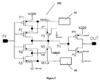
- Figure 5 shows a first embodiment of the compensated circuit according to the present invention, globally indicated by 200.
- the compensated circuit 200 has a basic structure similar to the trigger circuits already described with reference to the prior art solutions.
- the compensated circuit 200 comprises four input transistors P1, P2, N1 and N2 of the MOS type, in series to each other and connected between a first and a second voltage references, in particular a power supply voltage reference VDDS and a ground GND.
- the input transistors P1, P2, N1 and N2 are coupled by their respective gate electrodes to an input terminal IN of the compensated circuit 200. More particularly, the first and second input transistors P1 and P2 are PMOS transistors while the third and fourth input transistors N1 and N2 are NMOS transistors.
- the compensated circuit 200 also comprises further first and second control transistors, P3 and N3, of the MOS type, which realise a feedback structure to control the input PMOS and NMOS transistors.
- the first control transistor P3 is a PMOS transistor inserted between an interconnection node between the first and second input transistors P1 and P2 and the ground GND and has a gate terminal connected to the gate terminal of the second control transistor N3, which is in turn a NMOS transistor inserted between an interconnection node between the third and fourth input transistors N1 and N2 and the power supply voltage reference VDDS.
- VP or VN signals are generated at the interconnection nodes between the input transistors P1 and P2, respectively N1 and N2, such signals being controlled by the transistor size ratios P3/P1 and N3/N1.
- output transistors M 1 and M2 of the MOS type make an output inverter connected to an output terminal OUT of the compensated circuit 200.
- the output transistors M1 and M2 are inserted, in series to each other, between the power supply voltage reference VDDS and ground GND and have respective gate terminals connected to each other and to the common gate terminals of the control transistors P3 and N3, also indicated as node N.
- the first output transistor M 1 is of the PMOS type and has a bulk terminal connected to the power supply voltage VDDS and the second output transistor M2 is of the NMOS type and has a bulk terminal connected to ground GND.
- the first and second input transistors P1 and P2 as well as the first control transistor P3 of the compensated circuit 200 i.e. the transistors of the PMOS type, have bulk terminals connected together and to a first bulk control circuit 91 and receiving a NWELL signal.
- the third and fourth input transistors N 1 and N2 as well as the second control transistor N3 of the compensated circuit 200 i.e. the transistors of the NMOS type, have bulk terminals connected together and to a second bulk control circuit 95 and receiving a BULK signal.
- the threshold voltage of the NMOS and PMOS is controlled by the first and second bulk control circuits 91 & 95, according to the process variation of the circuit 200 itself.
- the bulk terminals of the NMOS transistors N1, N2, & N3 correspond to a substrate node, which is of P-type in a CMOS process while the bulk or nwell terminals of the PMOS transistors P1, P2 & P3 correspond to a substrate node, which is of N-type in a CMOS process.
- the high to low transition point Vil is determined by the ratio P 1 / P3 along with the NWELL signal.
- the low to high transition point Vih is determined by the ratio N1/N3 along with BULK signal.
- the NWELL and BULK signals can be generated by the bulk control circuits 91 and 95, respectively, such circuit being able to detect process variation.
- Figure 6 schematically shows a bulk control circuit 91 comprising a PMOS transistor M1p having same channel length as transistors P1 or P2 or P3.
- the transistor M1p is connected in diode configuration between the power supply voltage reference VDDS and a first control terminal providing the NWELL signal.
- the bulk control circuit 91 comprises a resistor R1' inserted between the first control terminal and ground GND, in series with the transistor M1p.
- the resistor R1 is required to set the bias current through the transistor M1p.
- the transistor M1p has a bulk terminal connected to the power supply voltage reference VDDS.
- the signal NWELL is at VDDS-
- This NWELL signal is also provided to the NWELL terminals of the PMOS transistors P1, P2 and P3, as shown in figure 5.
- the PMOS transistors P1, P2 and P3 have source-nwell and drain-nwell junction that form diodes. If the NWELL signal is below (VDDS-
- a grounded gate NMOS transistor M2p can be connected in place of the resistor R1, as shown in figure 8.
- the grounded gate NMOS transistor M2p has a bulk terminal and a gate terminal connected to the ground GND.
- the leakage current of the NMOS transistor M2p provides a ground path.
- the size of the NMOS transistor M2p should be kept large so that the leakage of the NMOS transistor M2p would be larger than the leakage of the NMOS transistor M1p in the OFF state.
- the NWELL signal is thus quickly pulled down to VDDS-
- the performance of the compensated circuit 200 would be dependent on the frequency of the input signal applied to the input terminal IN.
- the NWELL signal is dependent on the threshold voltage of the PMOS M1p that is again dependent on temperature and process. If process gets slow during fabrication, absolute threshold voltages of the PMOS transistors P1, P2 and P3 increases and change the value of transaction point voltage Vil. To keep the transaction point voltage Vil intact, threshold voltages of these PMOS transistors should be decreased. Since an increased value
- V t h V t h 0 + Y ( SQRT (
- Vth0 is the threshold voltage when Vsb is zero that is body effect is not present.
- two series PMOS transistors M1p and M3p can be used, as shown in figures 7 and 9.
- the effect of temperature and voltage is similar to the one correlated to the process. If the temperature increases, the threshold voltage of the PMOS transistors M1p and M3p would fall, which would increase the NWELL signal value and hence the threshold voltage of the PMOS transistors P1, P2 and P3 would increase to counterbalance the effect of increased temperature.
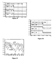
- the NWELL signal also changes as shown in the figure 19.
- the NWELL signal also makes a transition and settles at some value to stop DC current through the parasitic diodes of the PMOS transistors P1-P3.
- the NWELL signal is low when the signal at the input terminal IN is high, since the PMOS transistor P3 is ON and the channel-nwell junction also forms a diode increasing leakage current through the bulk terminals.
- the signal at the input terminal IN is low and the signal at the node N is high, which turns the PMOS transistor P3 OFF. This reduces the number of parallel paths for current through nwell and hence the NWELL signal rises.
- FIG. 10 Different embodiments of the bulk control circuit 95 according to the invention are shown in figures 10 to 13. These circuits generate the BULK signal for the control of the NMOS transistors N1, N2 and N3.
- Figure 10 schematically shows a bulk control circuit 91 comprising a NMOS transistor M1n which is connected in diode configuration between the a second control terminal providing the BULK signal and ground GND.
- the bulk control circuit 95 comprises a resistor R2 inserted between the power supply voltage reference VDDS and the second control terminal, in series with the transistor M1n.
- the transistor M1n has a bulk terminal connected to ground GND.
- a PMOS transistor M2n having a gate terminal connected to the power supply voltage reference VDDS can be connected in place of the resistor R2, as shown in figure 12.
- two series NMOS transistors M1n and M3n can be used, as shown in figures 11 and 13.
- the low to high transaction point Vih is determined by the ratio N1/N3 and by the BULK signal. Similar to the control of the NWELL signal, a control of the BULK signal is thus obtained. From the figures it is clear that when threshold voltage of the NMOS transistor M1n increases, either because of process or temperature variation, the BULK signal (which is proportional to the VtMln and VtM2n) increases and the threshold voltages of the NMOS transistors N1, N2 and N3 of the compensated circuit 200 decreases to stabilize the transaction point Vih.
- the BULK signal changes because of turn ON/OFF of the NMOS transistor N3 as shown in figure 20.
- the compensated circuit 200 comprising a threshold control, detects the change in process, temperature and voltage and controls the BULK and NWELL signals of the NMOS and PMOS transistors to neutralize the effect of the variation and therefore provides a very stable compensated circuit 200.
- the invention provides a self-adjusting circuit for bulk control in MOS devices against the PVT (process, voltage and temperature) variation.
- PVT process, voltage and temperature
- absolute threshold voltage values of all the transistors comprised in the circuit increases and the high to low transaction point Vil shifts towards ground (GND) while the low to high transaction point Vih shifts towards supply (VDDS).
- the compensated circuit according to the invention increases the hysteresis, but decreases the noise margin.
- the compensated circuit 200 is set to these values in the worst possible case.
- the high to low transaction point Vil is minimum when all the PMOS transistors are slow and all the NMOS transistors are fast while voltage and temperature is minimum
- the low to high transaction point Vih is maximum when all the NMOS transistors are slow and all the PMOS transistors are fast while voltage and temperature are maximum.
- hysteresis obtained is very low.
- the required hysteresis is not easily achieved or very low with the conventional circuits.
- the threshold voltage of the NMOS and PMOS transistors play major role at the device level in determining the high to low transaction point Vil and the low to high transaction point Vih, it is easy to stabilize the hysteresis if the threshold voltages of the MOS transistors can be controlled according to the PVT variation.
- Figure 14 shows a second embodiment of the compensated circuit 200 according to the invention, which employs bias blocks 97A and 97B, suitably connected to respective additional PVT detection circuits 98 and 99 to control the current drive while maintaining the threshold voltage.
- the additional PVT detection circuits 98 and 99 are drive control circuits.
- the first bias block 97A comprises a series of a first P4 and a second PMOS bias transistor P5 which are added in parallel with the first input PMOS transistor P1 to increase or decrease the current according to the PVT variation.
- the bias PMOS transistors P4 and P5 are connected, in series to each other, between the power supply voltage reference VDDS and the interconnection node between the first and second input PMOS transistors P1 and P2 and have respective bulk terminals also connected to the power supply voltage reference VDDS.
- the second bias PMOS transistor P5 has a gate terminal connected to the input terminal IN of the compensated circuit 200, while the first bias PMOS transistor P4 has a gate terminal connected to the first additional PVT detection circuit 98 and receive a first control signal PG therefrom.
- the second bias block 97B comprises a series of a first N4 and a second NMOS bias transistor N5 which are added in parallel with the first input NMOS transistor N 1 to increase or decrease the current according to the PVT variation.
- the bias NMOS transistors N4 and N5 are connected, in series to each other, between the interconnection node between the first and second input NMOS transistors N1 and N2 and ground GND have respective bulk terminals also connected to the ground GND.
- the second bias NMOS transistor N5 has a gate terminal connected to the input terminal IN of the compensated circuit 200, while the first bias NMOS transistor N4 has a gate terminal connected to the second additional PVT detection circuit 99 and receive a second control signal NG therefrom.
- the compensated circuit further comprises MOS transistors M1 and M2 to form an output inverter to provide sharp transition at the output terminal OUT.
- the bulk terminals of the NMOS transistors N1, N2 and N3 are connected to the bulk control circuit 91 and receive the signal BULK therefrom - as described earlier - while the bulk terminals of the PMOS transistors P1, P2 and P3 are connected to the bulk control circuit 95 and receive the signal NWELL therefrom.
- first additional PVT detection circuit 98 is shown in figures 15 and 16
- second additional PVT detection circuit 99 is shown in figures 17 and 18.
- the first additional PVT detection circuit 98 for generating the PG signal are similar to that of the bulk control circuit 91 for generating the NWELL signal, while the second additional PVT detection circuit 99 for generating the NG signal are similar to that of the bulk control circuit 95 for generating the BULK signal.
- figure 15 schematically shows the first additional PVT detection circuit 98 which comprises a first M1pg and a second PMOS transistor M2pg which are connected in diode configuration between the power supply voltage reference VDDS and a control terminal providing the PG signal.
- the first additional PVT detection circuit 98 comprises a resistor R1 inserted between the control terminal and ground GND, in series with the transistors M1pg and M2pg, according to a configuration increasing the insensitivity of the transaction point with respect to process variation.
- the transistors M1pg and M2pg have bulk terminals connected to the power supply voltage reference VDDS.
- NMOS transistor M3pg having a gate terminal connected to ground GND can be connected in place of the resistor R1, as shown in figure 16.
- figure 17 schematically shows the second additional PVT detection circuit 99 which comprises a first M1ng and a second NMOS transistor M2ng connected in diode configuration between a control terminal providing the NG signal and ground GND.
- the second additional PVT detection circuit 99 comprises a resistor R1ng inserted between the power supply voltage reference VDDS and the control terminal, in series with the transistors M1ng and M2ng, according to a configuration increasing the insensitivity of the transaction point with respect to process variation.
- the transistors M1ng and M2ng have bulk terminals connected to ground GND.
- a PMOS transistor M3ng having a gate terminal connected to the power supply voltage reference VDDS can be connected in place of the resistor R1ng, as shown in figure 17.
- the PMOS transistors P1, P2 and P5 are ON.
- the PMOS transistor P4 is also ON because its gate terminal is connected to the PG signal that is generated by the first additional PVT detection circuit 98.
- the voltage value of the PG signal would be (VDDS-
- the PMOS transistor P4 of the first bias block 97A is always ON.
- the voltage value of the PG signal changes according to the PVT variation. As the signal at the input terminal IN falls, the PMOS input transistors P1 and the second PMOS transistor P5 of the first bias block 97A turn ON and start charging the node VP.
- the voltage value of the high to low transaction point Vil is determined by the ratio (P1+P5)/P3 along with the NWELL and PG signals. When process gets slow or temperature increases, the driving of the transistors decreases and shifts the level of the high to low transaction point Vil towards ground GND or the high to low transaction point Vil should decrease.
- the signal PG also decreases and increases the driving of the first PMOS transistor P4 of the first bias block 97A and provides more current through the second PMOS transistor P5 of the first bias block 97A, the effect of temperature or process is counterbalanced. If voltage increases to increase the driving mechanism, the PG signal also increases to decrease the driving of the first PMOS transistor P4 of the first bias block 97A and hence the current is controlled. In this way the effect of PVT variation on current drive is neutralized up to certain extent and hence relatively more stable high to low transaction point Vil is achieved.
- the NMOS transistors N1, N2 and N5 are ON.
- the first NMOS transistor N4 of the second bias block 97B is also ON because its gate terminal is connected to the NG signal that is generated by the second additional PVT detection circuit 99.
- the voltage value of the NG signal will be (VtM 1+VtM2) provided the current through the NMOS transistors M1, M2 and M3 is very low.
- the first NMOS transistor N4 of the second bias block 97B is always ON.
- the voltage value of the NG signal will change according to the PVT variation.
- the first input NMOS transistor N1 and the second NMOS transistor N5 of the second bias block 97B turn ON and start charging the node VN.
- the voltage of the low to high transaction point Vih is determined by ratio (N1+N5)/N3 along with the BULK and NG signals.
- driving of the transistors decreases thus shifting the level of the low to high transaction point Vih towards the power supply voltage reference VDDS or the low to high transaction point Vih should increase.
- the invention thus relates to an apparatus for providing compensation against temperature, process and supply voltage variation in a MOS circuit comprising:
- the apparatus should comprise:
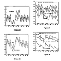
- x-axis represents the PVT variation, where process, voltage and temperature are varying together.
- PVT all possible combinations of 3-voltages, 3-tempetatures and 5-processes
- SLOW indicates the process when the PMOS transistors and the NMOS transistors both are slow (3-sigma).
- NFPS indicates the process when NMOS transistors are fast (6-sigma) and PMOS transistors are slow (6-sigma).
- NSPF indicates the process when NMOS transistors are slow (6-sigma) and PMOS transistors are fast (6-sigma).
- TYP indicates the centered process.
- FAST indicates the process when NMOS and PMOS transistors both are fast (3-sigma).
- the graphs shown in figure 27 and 28 compare a standard structure with the proposed compensated circuit with Vth (threshold voltage of MOSFETES) control and the proposed compensated circuit with Vth and current control respectively.
Landscapes
- Physics & Mathematics (AREA)
- Engineering & Computer Science (AREA)
- Computer Hardware Design (AREA)
- Computing Systems (AREA)
- General Engineering & Computer Science (AREA)
- Mathematical Physics (AREA)
- Logic Circuits (AREA)
- Metal-Oxide And Bipolar Metal-Oxide Semiconductor Integrated Circuits (AREA)
- Semiconductor Integrated Circuits (AREA)
- Control Of Electrical Variables (AREA)
Applications Claiming Priority (1)
| Application Number | Priority Date | Filing Date | Title |
|---|---|---|---|
| IN2384DE2004 | 2004-11-29 |
Publications (2)
| Publication Number | Publication Date |
|---|---|
| EP1662660A2 true EP1662660A2 (de) | 2006-05-31 |
| EP1662660A3 EP1662660A3 (de) | 2007-12-12 |
Family
ID=35986626
Family Applications (1)
| Application Number | Title | Priority Date | Filing Date |
|---|---|---|---|
| EP05025953A Ceased EP1662660A3 (de) | 2004-11-29 | 2005-11-29 | Verfahren und Gerät zum Kompensieren gegen Temperatur-, Spannungs- und Herstellungsschwankungen |
Country Status (2)
| Country | Link |
|---|---|
| US (1) | US7368976B2 (de) |
| EP (1) | EP1662660A3 (de) |
Cited By (2)
| Publication number | Priority date | Publication date | Assignee | Title |
|---|---|---|---|---|
| EP2933920A4 (de) * | 2012-12-17 | 2016-07-27 | Smarter Microelectronics Guang Zhou Co Ltd | Kleine schnelle flip-flop-schmitt-schaltung für soi- verfahren |
| EP2560284A3 (de) * | 2011-08-19 | 2017-05-17 | Altera Corporation | Vorrichtung zur Verbesserung der Leistung von feldprogrammierbaren Gate-Arrays und dazugehörige Verfahren |
Families Citing this family (30)
| Publication number | Priority date | Publication date | Assignee | Title |
|---|---|---|---|---|
| JP5184760B2 (ja) * | 2006-06-05 | 2013-04-17 | ラピスセミコンダクタ株式会社 | 電流駆動回路 |
| US7554853B2 (en) * | 2006-12-30 | 2009-06-30 | Sandisk Corporation | Non-volatile storage with bias based on selective word line |
| US7525843B2 (en) * | 2006-12-30 | 2009-04-28 | Sandisk Corporation | Non-volatile storage with adaptive body bias |
| US7468919B2 (en) * | 2006-12-30 | 2008-12-23 | Sandisk Corporation | Biasing non-volatile storage based on selected word line |
| US7583539B2 (en) * | 2006-12-30 | 2009-09-01 | Sandisk Corporation | Non-volatile storage with bias for temperature compensation |
| US7583535B2 (en) * | 2006-12-30 | 2009-09-01 | Sandisk Corporation | Biasing non-volatile storage to compensate for temperature variations |
| US7468920B2 (en) | 2006-12-30 | 2008-12-23 | Sandisk Corporation | Applying adaptive body bias to non-volatile storage |
| KR100862113B1 (ko) * | 2007-01-22 | 2008-10-09 | 삼성전자주식회사 | 공정 변화에 대한 정보를 이용하여 공급전압/공급주파수를제어할 수 있는 장치와 방법 |
| US7605601B2 (en) * | 2007-04-19 | 2009-10-20 | Kabushiki Kaisha Toshiba | Semiconductor integrated circuit device |
| US7606072B2 (en) * | 2007-04-24 | 2009-10-20 | Sandisk Corporation | Non-volatile storage with compensation for source voltage drop |
| US7606071B2 (en) * | 2007-04-24 | 2009-10-20 | Sandisk Corporation | Compensating source voltage drop in non-volatile storage |
| US9654108B2 (en) * | 2008-01-11 | 2017-05-16 | Intel Mobile Communications GmbH | Apparatus and method having reduced flicker noise |
| US7936208B2 (en) * | 2008-07-31 | 2011-05-03 | International Business Machines Corporation | Bias circuit for a MOS device |
| CN101819449B (zh) * | 2010-04-16 | 2012-01-04 | 上海理工大学 | 亚阈值mosfet带隙基准源 |
| US8411525B2 (en) * | 2010-04-29 | 2013-04-02 | Taiwan Semiconductor Manufacturing Company, Ltd. | Memory circuits having a diode-connected transistor with back-biased control |
| US8081026B1 (en) | 2010-05-26 | 2011-12-20 | Freescale Semiconductor, Inc. | Method for supplying an output supply voltage to a power gated circuit and an integrated circuit |
| US20100321094A1 (en) * | 2010-08-29 | 2010-12-23 | Hao Luo | Method and circuit implementation for reducing the parameter fluctuations in integrated circuits |
| KR101318423B1 (ko) * | 2011-06-24 | 2013-10-15 | 위니맥스 주식회사 | 정수필터 어셈블리 및 이를 구비한 냉장고 및 정수기 |
| US8461869B1 (en) * | 2011-08-19 | 2013-06-11 | Altera Corporation | Apparatus for configuring performance of field programmable gate arrays and associated methods |
| US8618842B2 (en) | 2011-09-30 | 2013-12-31 | Qualcomm Incorporated | Differential PVT/timing-skew-tolerant self-correcting circuits |
| US8975952B2 (en) * | 2012-11-13 | 2015-03-10 | Honeywell International Inc. | CMOS logic circuit using passive internal body tie bias |
| KR20150029262A (ko) * | 2013-09-10 | 2015-03-18 | 삼성전자주식회사 | 이미지 센서, 이를 포함하는 이미지 처리 시스템 및 이의 동작 방법 |
| JP6767225B2 (ja) | 2016-09-29 | 2020-10-14 | ルネサスエレクトロニクス株式会社 | 半導体装置 |
| CN108155901B (zh) * | 2016-12-05 | 2023-11-24 | 中国工程物理研究院电子工程研究所 | 一种抗参数漂移反相器 |
| CN106972850A (zh) * | 2017-03-03 | 2017-07-21 | 安徽大学 | 一种具有抗单粒子瞬态效应的反相器 |
| US10685703B2 (en) | 2018-09-12 | 2020-06-16 | Nxp B.V. | Transistor body bias control circuit for SRAM cells |
| WO2021111772A1 (ja) * | 2019-12-03 | 2021-06-10 | 富士電機株式会社 | 比較回路、半導体装置 |
| US11074946B2 (en) * | 2019-12-05 | 2021-07-27 | Nxp B.V. | Temperature dependent voltage differential sense-amplifier |
| US11444611B2 (en) | 2020-10-06 | 2022-09-13 | Mediatek Inc. | Chip having a receiver including a hysteresis circuit |
| CN113674694B (zh) * | 2021-08-23 | 2023-09-01 | 京东方科技集团股份有限公司 | 显示基板及显示装置 |
Citations (1)
| Publication number | Priority date | Publication date | Assignee | Title |
|---|---|---|---|---|
| US6147508A (en) | 1998-08-20 | 2000-11-14 | International Business Machines Corp. | Power consumption control mechanism and method therefor |
Family Cites Families (7)
| Publication number | Priority date | Publication date | Assignee | Title |
|---|---|---|---|---|
| US5017811A (en) * | 1989-10-27 | 1991-05-21 | Rockwell International Corporation | CMOS TTL input buffer using a ratioed inverter with a threshold voltage adjusted N channel field effect transistor |
| US5461338A (en) * | 1992-04-17 | 1995-10-24 | Nec Corporation | Semiconductor integrated circuit incorporated with substrate bias control circuit |
| US5406144A (en) * | 1993-09-07 | 1995-04-11 | Texas Instruments Incorporated | Power reduction in a temperature compensating transistor circuit |
| KR0169157B1 (ko) * | 1993-11-29 | 1999-02-01 | 기다오까 다까시 | 반도체 회로 및 mos-dram |
| JP2822881B2 (ja) * | 1994-03-30 | 1998-11-11 | 日本電気株式会社 | 半導体集積回路装置 |
| JP3614546B2 (ja) * | 1995-12-27 | 2005-01-26 | 富士通株式会社 | 半導体集積回路 |
| GB2340682B (en) * | 1998-08-10 | 2003-11-05 | Sgs Thomson Microelectronics | Variable threshold inverter |
-
2005
- 2005-11-29 EP EP05025953A patent/EP1662660A3/de not_active Ceased
- 2005-11-29 US US11/290,619 patent/US7368976B2/en not_active Expired - Fee Related
Patent Citations (1)
| Publication number | Priority date | Publication date | Assignee | Title |
|---|---|---|---|---|
| US6147508A (en) | 1998-08-20 | 2000-11-14 | International Business Machines Corp. | Power consumption control mechanism and method therefor |
Cited By (2)
| Publication number | Priority date | Publication date | Assignee | Title |
|---|---|---|---|---|
| EP2560284A3 (de) * | 2011-08-19 | 2017-05-17 | Altera Corporation | Vorrichtung zur Verbesserung der Leistung von feldprogrammierbaren Gate-Arrays und dazugehörige Verfahren |
| EP2933920A4 (de) * | 2012-12-17 | 2016-07-27 | Smarter Microelectronics Guang Zhou Co Ltd | Kleine schnelle flip-flop-schmitt-schaltung für soi- verfahren |
Also Published As
| Publication number | Publication date |
|---|---|
| US20060226889A1 (en) | 2006-10-12 |
| US7368976B2 (en) | 2008-05-06 |
| EP1662660A3 (de) | 2007-12-12 |
Similar Documents
| Publication | Publication Date | Title |
|---|---|---|
| EP1662660A2 (de) | Verfahren und Gerät zum Kompensieren gegen Temperatur-, Spannungs- und Herstellungsschwankungen | |
| US6853217B2 (en) | Level conversion circuit and semiconductor integrated circuit device employing the level conversion circuit | |
| US6791391B2 (en) | Level shifting circuit | |
| US20070115041A1 (en) | Level conversion circuit | |
| US7898321B2 (en) | Driver circuit | |
| US7173472B2 (en) | Input buffer structure with single gate oxide | |
| KR20010049227A (ko) | 레벨조정회로 및 이를 포함하는 데이터 출력회로 | |
| US7482847B2 (en) | Power-on reset circuit | |
| US11245388B2 (en) | Level shifter circuitry using current mirrors | |
| KR100885830B1 (ko) | 리미터 회로 | |
| US6559676B1 (en) | Output buffer circuit | |
| US6784700B1 (en) | Input buffer circuit | |
| US6753707B2 (en) | Delay circuit and semiconductor device using the same | |
| EP0541242A1 (de) | Komplementäre MOSFET-Pufferschaltung für digitale Signale mit geringem Verbrauch | |
| JP2011103607A (ja) | 入力回路 | |
| KR100300687B1 (ko) | 반도체집적회로 | |
| US7663403B2 (en) | High-speed asynchronous digital signal level conversion circuit | |
| US9608604B2 (en) | Voltage level shifter with single well voltage | |
| US7755407B2 (en) | Variable delay circuit, testing apparatus, and electronic device | |
| US20230080713A1 (en) | Level shifter and chip with overdrive capability | |
| US20020153944A1 (en) | Semiconductor integrated circuit | |
| US7737734B1 (en) | Adaptive output driver | |
| JP2006295322A (ja) | レベルシフタ回路 | |
| KR102617255B1 (ko) | 전자 장치 및 그의 동작 방법 | |
| US7053671B1 (en) | Low-jitter differential-to-single-ended data conversion circuits |
Legal Events
| Date | Code | Title | Description |
|---|---|---|---|
| PUAI | Public reference made under article 153(3) epc to a published international application that has entered the european phase |
Free format text: ORIGINAL CODE: 0009012 |
|
| AK | Designated contracting states |
Kind code of ref document: A2 Designated state(s): AT BE BG CH CY CZ DE DK EE ES FI FR GB GR HU IE IS IT LI LT LU LV MC NL PL PT RO SE SI SK TR |
|
| AX | Request for extension of the european patent |
Extension state: AL BA HR MK YU |
|
| PUAL | Search report despatched |
Free format text: ORIGINAL CODE: 0009013 |
|
| AK | Designated contracting states |
Kind code of ref document: A3 Designated state(s): AT BE BG CH CY CZ DE DK EE ES FI FR GB GR HU IE IS IT LI LT LU LV MC NL PL PT RO SE SI SK TR |
|
| AX | Request for extension of the european patent |
Extension state: AL BA HR MK YU |
|
| RIC1 | Information provided on ipc code assigned before grant |
Ipc: H03K 17/14 20060101ALI20071102BHEP Ipc: H03K 3/011 20060101ALI20071102BHEP Ipc: H03K 19/003 20060101AFI20060317BHEP |
|
| 17P | Request for examination filed |
Effective date: 20080611 |
|
| 17Q | First examination report despatched |
Effective date: 20080716 |
|
| AKX | Designation fees paid |
Designated state(s): AT BE BG CH LI |
|
| REG | Reference to a national code |
Ref country code: DE Ref legal event code: 8566 |
|
| STAA | Information on the status of an ep patent application or granted ep patent |
Free format text: STATUS: THE APPLICATION HAS BEEN REFUSED |
|
| 18R | Application refused |
Effective date: 20091006 |