EP1663852B1 - Procédé d'individualisation de composants - Google Patents
Procédé d'individualisation de composants Download PDFInfo
- Publication number
- EP1663852B1 EP1663852B1 EP04738871A EP04738871A EP1663852B1 EP 1663852 B1 EP1663852 B1 EP 1663852B1 EP 04738871 A EP04738871 A EP 04738871A EP 04738871 A EP04738871 A EP 04738871A EP 1663852 B1 EP1663852 B1 EP 1663852B1
- Authority
- EP
- European Patent Office
- Prior art keywords
- germanium
- etching
- containing layer
- layer
- etching process
- Prior art date
- Legal status (The legal status is an assumption and is not a legal conclusion. Google has not performed a legal analysis and makes no representation as to the accuracy of the status listed.)
- Expired - Lifetime
Links
Images

Classifications
-
- B—PERFORMING OPERATIONS; TRANSPORTING
- B81—MICROSTRUCTURAL TECHNOLOGY
- B81C—PROCESSES OR APPARATUS SPECIALLY ADAPTED FOR THE MANUFACTURE OR TREATMENT OF MICROSTRUCTURAL DEVICES OR SYSTEMS
- B81C1/00—Manufacture or treatment of devices or systems in or on a substrate
- B81C1/00015—Manufacture or treatment of devices or systems in or on a substrate for manufacturing microsystems
- B81C1/00023—Manufacture or treatment of devices or systems in or on a substrate for manufacturing microsystems without movable or flexible elements
- B81C1/00055—Grooves
- B81C1/00063—Trenches
-
- H—ELECTRICITY
- H10—SEMICONDUCTOR DEVICES; ELECTRIC SOLID-STATE DEVICES NOT OTHERWISE PROVIDED FOR
- H10D—INORGANIC ELECTRIC SEMICONDUCTOR DEVICES
- H10D64/00—Electrodes of devices having potential barriers
- H10D64/01—Manufacture or treatment
- H10D64/011—Manufacture or treatment of electrodes ohmically coupled to a semiconductor
-
- B—PERFORMING OPERATIONS; TRANSPORTING
- B81—MICROSTRUCTURAL TECHNOLOGY
- B81C—PROCESSES OR APPARATUS SPECIALLY ADAPTED FOR THE MANUFACTURE OR TREATMENT OF MICROSTRUCTURAL DEVICES OR SYSTEMS
- B81C1/00—Manufacture or treatment of devices or systems in or on a substrate
- B81C1/00865—Multistep processes for the separation of wafers into individual elements
- B81C1/00888—Multistep processes involving only mechanical separation, e.g. grooving followed by cleaving
Definitions
- the invention relates to a method for separating components based on silicon or a layered structure of silicon / insulator according to the preamble of claim 1.
- etching holes or etching trenches are relatively deep into a substrate, e.g. into a wafer or possibly completely through the substrate.
- complete penetration e.g. A wafer is not readily available in most processes.
- a method is known in which a silicon wafer is etched from the rear side at the locations where a continuous trench or through-hole is to be formed to a predetermined uncritical depth, for example with the aid of a KOH etching process. Subsequently, the resulting etching structures are filled with a paint, such as photoresist. Furthermore, from the front can be easily the through trench or through-hole is etched into the wafer, which serves as an etch stop and at the same time prevents etching medium from passing through the wafer onto the back side of the wafer into a corresponding area of the process plant or wafer clamping device, thereby stopping the process or the corresponding units are contaminated.
- the invention has for its object to provide a method for separating components.
- the invention is initially based on a method for producing etching holes and / or etching trenches of components based on silicon or a layer structure of silicon / insulator.
- the essence of the invention lies in the fact that a germanium-containing layer and / or a germanium layer is provided at the location at which or in the vicinity of which an etching process in the silicon or an insulator is to be terminated, that during the etching process Detection is carried out on germanium and / or germanium compounds and that, depending on the detection of germanium and / or germanium compounds, the etching process is controlled, in particular stopped.
- This procedure is based on the finding that germanium or germanium compounds can be detected comparatively well in an etching process with respect to etching products during the etching of silicon or insulators commonly used in the semiconductor field.
- a mass spectrometer or an optical emission spectrometer eg for the evaluation of an etching plasma, can be used.
- etching plasma based on fluorochemistry with an optical emission spectrometer after the occurrence of a GeF x line is monitored to determine the achievement of a germanium or germanium-containing layer.
- the emergence of a relevant line in the spectrum can be used as a "stop criterion" for the etching process, namely, when appropriate ⁇ tzgräben or etching holes to be introduced to the corresponding germanium or germanium-containing layer in eg a wafer.
- the germanium and / or germanium-containing layer is applied on the back side of a silicon wafer.
- an etching trench can be etched through the entire wafer by means of customary plasma etching processes, with the detection of germanium etch products making it easy to determine the complete throughput through the wafer.
- the etching is stopped, so that there is still no complete passage on the back side of the wafer.
- the germanium layer is a protective barrier, so that no For example, etching medium can get to a wafer clamping device on the back of the wafer or a holder of the wafer, for example, with a vacuum chuck is still possible.
- a germanium layer or a germanium-containing layer can be removed, for example, selectively with respect to silicon or common insulators used in semiconductor technology with the aid of hydrogen peroxide or hydrogen peroxide-containing etching solutions.
- a germanium or germanium containing layer e.g. a germanium-containing silicon layer (SiGe) can be deposited by means of CVD (Chemical Vapor Deposition) or PECVD (Plasma Enhanced Chemical Vapor Deposition), if this is compatible with the overall process, in particular preceding process steps.
- a germanium or germanium-containing layer can also be sputtered on, which is possible at comparatively lower temperatures.
- the germanium-containing layer may be coated with a metal capping layer, such as e.g. Tungsten-titanium. This has advantages in terms of contamination prevention.
- the germanium and / or germanium-containing layer which is applied to the backside of a wafer is advantageously used for singulating electronic components from the wafer by producing completely penetrating trenches in the wafer up to the germanium layer and then removing the germanium layer in a subsequent step Individual components corresponding to the etching trenches arise as a cohesion is no longer present by the back germanium and / or germanium-containing layer after their removal.
- the germanium and / or germanium-containing layer can also be buried in a layer structure.
- the germanium and / or germanium-containing layer can be used selectively as an "etch stop" layer by detecting germanium or germanium compounds during etching processes in a layer arranged above or a plurality of layers arranged above it (containing no germanium) , In this way, e.g. "Trench etching processes” or etching processes for generating a cavern defined to be made.
- a buried germanium and / or germanium-containing layer in the layer structure can be used simultaneously as a device function layer.
- this layer can be used as a membrane which can be formed in one or more etching processes by removal of adjacent material, such as e.g. Silicon or silicon-containing oxides is formed. Such a process is reliably possible by the comparatively exact detectability of reaching the germanium and / or germanium-containing layer.
- a germanium and / or germanium-containing layer can be used for the control of a lateral and / or vertical etching process on a substrate.
- FIG. 1 is shown in section an SOI wafer 1.
- the SOI wafer 1 consists of functional silicon 2 and an SOI oxide layer 3 on bulk silicon 4.
- FIG. 2 the layer structure after the structuring of the functional silicon 2 into partial regions 2a is shown with the aid of a photoresist mask 5 by an anisotropic etching process.
- the functional layer 2 was trimmed to the SOI oxide layer 3 (etched through).
- FIG. 3 shows a process stage according to the following steps:
- the resist mask 4 has been removed. Between the functional silicon regions 2 a, the "trimmed" regions 7 were filled with a filler oxide 6 and the filler oxide 6 was opened again in contact regions 8 via a further mask / photolithography step. In two subsequent sputtering steps, firstly the metallization for the contacts 8 on the front side and secondly a germanium layer 9 on the back side of the wafer 1 were sputtered on. Via another mask / photolithography process, the contact plane was structured in a metal dry etching process, for example. As result This process series remains the structured contact metal. 8
- a PECVD protective oxide layer 10 has been applied to the layer structure and the regions at which a "trench” is to be etched through the wafer 1 are defined by means of a photolithography process step.
- customary "trench processes” can be used for the etching of a trench 11.
- the trench 11 was etched through the layer structure of thin protective oxide 10, filler oxide 6, functional silicon 2a, thin SOI oxide 3 and thick bulk silicon 4.
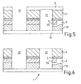
- FIG. 5 For example, the wafer fixed for sawing on blue tape 12 is depicted with an already sawed sawing road 13. The wafer 1 was fixed with the front on the "blue tape”.
- FIG. 6 shows the process stage with the germanium layer 9 removed.
- a hydrogen peroxide solution can be used, for example, in the manner of a spray developer.
- the individual components formed on the wafer can then be separated by removal from the "blue tape" 12.
Landscapes
- Engineering & Computer Science (AREA)
- Manufacturing & Machinery (AREA)
- Microelectronics & Electronic Packaging (AREA)
- Chemical & Material Sciences (AREA)
- Analytical Chemistry (AREA)
- Weting (AREA)
- Drying Of Semiconductors (AREA)
- Micromachines (AREA)
- Pressure Sensors (AREA)
- Testing Or Measuring Of Semiconductors Or The Like (AREA)
Claims (7)
- Procédé pour séparer un à un des composants à base de silicium ou d'une structure stratifiée de silicium et d'isolant, dans lequel une couche contenant du germanium et/ou une couche (9) de germanium est prévue en un emplacement d'un substrat sur lequel ou au voisinage duquel une opération de gravure doit se terminer,
l'opération de gravure formant des rainures gravées (11) sur le côté avant du substrat et les produits de gravure du germanium étant détectés pendant l'opération de gravure, l'opération de gravure étant interrompue en cas de détection du germanium et/ou du composé de germanium,
caractérisé en ce que
la couche (9) en germanium ou contenant du germanium est appliquée sur le côté arrière du substrat et est enlevée lorsque l'opération de gravure est terminée, pour séparer les différents composants en correspondance aux rainures gravées (11). - Procédé selon la revendication 1, caractérisé en ce que la couche (9) en germanium et/ou contenant du germanium est formée par CVD ("Chemical Vapor Déposition" - dépôt chimique de vapeur), en particulier par PECVD ("Plasma Enhanced Chemical Vapor Deposition"- dépôt chimique de vapeur renforcé par plasma) ou par pulvérisation.
- Procédé selon les revendications 1 ou 2, caractérisé en ce que la couche (9) en germanium et/ou contenant du germanium est enlevée au moyen de peroxyde d'hydrogène ou d'une solution de gravure contenant du peroxyde d'hydrogène, en particulier par un développeur à aspersion.
- Procédé selon l'une des revendications précédentes, caractérisé en ce que l'on y détecte le germanium et/ou les composés de germanium par spectroscopie à émission optique ou par spectroscopie de masse.
- Procédé selon l'une des revendications précédentes, caractérisé en ce qu'avant d'enlever la couche (9) en germanium et/ou contenant du germanium, le substrat est fixé sur une feuille par son côté avant.
- Procédé selon la revendication 5, caractérisé en ce qu'avant d'enlever la couche (9) en germanium et/ou contenant du germanium, le substrat est scié de manière à former des pistes sciées (13).
- Procédé selon les revendications 5 ou 6, caractérisé en ce que les différents composants sont retirés de la feuille après l'enlèvement de la couche (9) en germanium et/ou contenant du germanium.
Applications Claiming Priority (2)
| Application Number | Priority Date | Filing Date | Title |
|---|---|---|---|
| DE10342155A DE10342155A1 (de) | 2003-09-12 | 2003-09-12 | Verfahren zur Herstellung von Ätzlöchern und/oder Ätzgräben sowie Membransensoreinheit |
| PCT/DE2004/001449 WO2005026041A1 (fr) | 2003-09-12 | 2004-07-07 | Procede de production de trous graves et/ou de tranchees gravees, et unite detectrice a membrane |
Publications (2)
| Publication Number | Publication Date |
|---|---|
| EP1663852A1 EP1663852A1 (fr) | 2006-06-07 |
| EP1663852B1 true EP1663852B1 (fr) | 2008-12-31 |
Family
ID=34258603
Family Applications (1)
| Application Number | Title | Priority Date | Filing Date |
|---|---|---|---|
| EP04738871A Expired - Lifetime EP1663852B1 (fr) | 2003-09-12 | 2004-07-07 | Procédé d'individualisation de composants |
Country Status (6)
| Country | Link |
|---|---|
| US (1) | US20070087464A1 (fr) |
| EP (1) | EP1663852B1 (fr) |
| KR (1) | KR20060119961A (fr) |
| DE (2) | DE10342155A1 (fr) |
| TW (1) | TW200511426A (fr) |
| WO (1) | WO2005026041A1 (fr) |
Families Citing this family (2)
| Publication number | Priority date | Publication date | Assignee | Title |
|---|---|---|---|---|
| US9275916B2 (en) * | 2013-05-03 | 2016-03-01 | Infineon Technologies Ag | Removable indicator structure in electronic chips of a common substrate for process adjustment |
| DE102017213631A1 (de) | 2017-08-07 | 2019-02-07 | Robert Bosch Gmbh | Mikromechanische Vorrichtung und entsprechendes Herstellungsverfahren |
Citations (2)
| Publication number | Priority date | Publication date | Assignee | Title |
|---|---|---|---|---|
| US5961877A (en) * | 1994-11-10 | 1999-10-05 | Robinson; Mcdonald | Wet chemical etchants |
| DE10102993A1 (de) * | 2001-01-24 | 2002-07-25 | Bosch Gmbh Robert | Herstellungsverfahren für ein mikromechanisches Bauelement |
Family Cites Families (16)
| Publication number | Priority date | Publication date | Assignee | Title |
|---|---|---|---|---|
| US4093933A (en) * | 1976-05-14 | 1978-06-06 | Becton, Dickinson Electronics Company | Sculptured pressure diaphragm |
| GB8402654D0 (en) * | 1984-02-01 | 1984-03-07 | Secr Defence | Flatpanel display |
| JP2544435B2 (ja) * | 1988-04-06 | 1996-10-16 | 株式会社日立製作所 | 多機能センサ |
| US5335210A (en) * | 1992-10-28 | 1994-08-02 | The Charles Stark Draper Laboratory Inc. | Integrated liquid crystal acoustic transducer |
| US5413679A (en) * | 1993-06-30 | 1995-05-09 | The United States Of America As Represented By The Secretary Of The Navy | Method of producing a silicon membrane using a silicon alloy etch stop layer |
| US5310451A (en) * | 1993-08-19 | 1994-05-10 | International Business Machines Corporation | Method of forming an ultra-uniform silicon-on-insulator layer |
| US5904546A (en) * | 1996-02-12 | 1999-05-18 | Micron Technology, Inc. | Method and apparatus for dicing semiconductor wafers |
| US5888845A (en) * | 1996-05-02 | 1999-03-30 | National Semiconductor Corporation | Method of making high sensitivity micro-machined pressure sensors and acoustic transducers |
| US6159385A (en) * | 1998-05-08 | 2000-12-12 | Rockwell Technologies, Llc | Process for manufacture of micro electromechanical devices having high electrical isolation |
| US6198098B1 (en) * | 1998-05-26 | 2001-03-06 | Philips Laou | Microstructure for infrared detector and method of making same |
| WO2000042231A2 (fr) * | 1999-01-15 | 2000-07-20 | The Regents Of The University Of California | Films de polysilicium-germanium permettant de realiser des systemes micro-electromecaniques |
| KR100392166B1 (ko) * | 2000-03-17 | 2003-07-22 | 가부시끼가이샤 도시바 | 반도체 장치의 제조 방법 및 반도체 장치 |
| US7535100B2 (en) * | 2002-07-12 | 2009-05-19 | The United States Of America As Represented By The Secretary Of The Navy | Wafer bonding of thinned electronic materials and circuits to high performance substrates |
| US20040087054A1 (en) * | 2002-10-18 | 2004-05-06 | Applied Materials, Inc. | Disposable barrier technique for through wafer etching in MEMS |
| US6908846B2 (en) * | 2002-10-24 | 2005-06-21 | Lam Research Corporation | Method and apparatus for detecting endpoint during plasma etching of thin films |
| US6936491B2 (en) * | 2003-06-04 | 2005-08-30 | Robert Bosch Gmbh | Method of fabricating microelectromechanical systems and devices having trench isolated contacts |
-
2003
- 2003-09-12 DE DE10342155A patent/DE10342155A1/de not_active Withdrawn
-
2004
- 2004-07-07 DE DE502004008787T patent/DE502004008787D1/de not_active Expired - Lifetime
- 2004-07-07 WO PCT/DE2004/001449 patent/WO2005026041A1/fr not_active Ceased
- 2004-07-07 KR KR1020067004970A patent/KR20060119961A/ko not_active Ceased
- 2004-07-07 US US10/571,246 patent/US20070087464A1/en not_active Abandoned
- 2004-07-07 EP EP04738871A patent/EP1663852B1/fr not_active Expired - Lifetime
- 2004-07-14 TW TW093120949A patent/TW200511426A/zh unknown
Patent Citations (2)
| Publication number | Priority date | Publication date | Assignee | Title |
|---|---|---|---|---|
| US5961877A (en) * | 1994-11-10 | 1999-10-05 | Robinson; Mcdonald | Wet chemical etchants |
| DE10102993A1 (de) * | 2001-01-24 | 2002-07-25 | Bosch Gmbh Robert | Herstellungsverfahren für ein mikromechanisches Bauelement |
Also Published As
| Publication number | Publication date |
|---|---|
| KR20060119961A (ko) | 2006-11-24 |
| DE10342155A1 (de) | 2005-04-07 |
| DE502004008787D1 (de) | 2009-02-12 |
| TW200511426A (en) | 2005-03-16 |
| EP1663852A1 (fr) | 2006-06-07 |
| US20070087464A1 (en) | 2007-04-19 |
| WO2005026041A1 (fr) | 2005-03-24 |
Similar Documents
| Publication | Publication Date | Title |
|---|---|---|
| DE69912376T2 (de) | Verfahren zur herstellung eines halbleiterbauelements | |
| DE102014106132B4 (de) | Verfahren und Vorrichtung zur Verarbeitung einer Mehrzahl von gehäusten elektronischen Chips, elektronischer Chip, umfassend eine Indikatorschicht, und Artikel, umfassend eine Mehrzahl derartiger elektronischer Chips | |
| DE69508816T2 (de) | Substrat für integrierte Bauelemente mit einer Dünnschicht und Herstellungsverfahren | |
| DE102005007540A1 (de) | Mikromechanischer Membransensor mit Doppelmembran | |
| DE19715194B4 (de) | Verfahren zum Herstellen von Halbleitervorrichtungen unter Verwendung von Trockenätzen | |
| DE10031252A1 (de) | Verfahren zur Zertrennung eines Substratwafers in eine Anzahl von Substratchips | |
| DE102012208033A1 (de) | Hybrid integriertes Bauteil und Verfahren zu dessen Herstellung | |
| DE10051890A1 (de) | Halbleiterwaferteilungsverfahren | |
| DE102018124822A1 (de) | Verfahren zum herstellen eines mems-packages mit mehreren tiefen | |
| DE102020101520B4 (de) | Halbleitervorrichtung und verfahren | |
| DE102020213030A1 (de) | Herstellungsverfahren für ein mikromechanisches Bauteil für eine Sensor- oder Mikrofonvorrichtung | |
| DE102018221108A1 (de) | Verfahren zum Einstellen eines Drucks in einer mithilfe eines Substrats und einer Substratkappe ausgebildeten Kaverne, Halbleitersystem, insbesondere Wafersystem | |
| EP0906578B1 (fr) | Detecteur d'une valeur limite d'acceleration | |
| DE102019202794B3 (de) | Mikromechanische Sensorvorrichtung und entsprechendes Herstellungsverfahren | |
| DE102013111008A1 (de) | Silizium-auf-Nichts-Einheiten und Verfahren für ihre Herstellung | |
| DE102010061782B4 (de) | Verfahren zum Herstellen eines mikromechanischen Bauelements | |
| DE102005008750B4 (de) | Struktur zum Enthalten von Trocknungsmitteln, Verfahren zum Herstellen und Verwendung der Struktur | |
| WO2010060684A2 (fr) | Procédé de fabrication d'un composant micromécanique, composant micromécanique fabriqué selon ce procédé et son utilisation | |
| DE102013109375B4 (de) | Verfahren zum verarbeiten eines wafers | |
| DE102015223399B4 (de) | Verfahren zum Verpacken mindestens eines Halbleiterbauteils und Halbleitervorrichtung | |
| DE10342155A1 (de) | Verfahren zur Herstellung von Ätzlöchern und/oder Ätzgräben sowie Membransensoreinheit | |
| DE102013109590A1 (de) | Verfahren zum Bearbeiten eines Wafers und Verfahren zum Zertrennen eines Wafers | |
| EP2150488B1 (fr) | Procédé de fabrication d'un composant micromécanique comportant une couche de charge et une couche de masque | |
| DE102017213636A1 (de) | Verfahren zur Herstellung von dünnen MEMS Chips auf SOI Substrat und mikromechanisches Bauelement | |
| DE102023201034A1 (de) | Verfahren zur Herstellung einer mikromechanischen Vorrichtung mit einer Kaverne mit einem Schmelzverschluss |
Legal Events
| Date | Code | Title | Description |
|---|---|---|---|
| PUAI | Public reference made under article 153(3) epc to a published international application that has entered the european phase |
Free format text: ORIGINAL CODE: 0009012 |
|
| 17P | Request for examination filed |
Effective date: 20060412 |
|
| AK | Designated contracting states |
Kind code of ref document: A1 Designated state(s): DE FR GB |
|
| 17Q | First examination report despatched |
Effective date: 20060720 |
|
| DAX | Request for extension of the european patent (deleted) | ||
| RBV | Designated contracting states (corrected) |
Designated state(s): DE FR GB |
|
| GRAP | Despatch of communication of intention to grant a patent |
Free format text: ORIGINAL CODE: EPIDOSNIGR1 |
|
| RTI1 | Title (correction) |
Free format text: METHOD FOR SINGULATING DEVICES |
|
| RTI1 | Title (correction) |
Free format text: METHOD FOR SINGULATING DEVICES |
|
| GRAS | Grant fee paid |
Free format text: ORIGINAL CODE: EPIDOSNIGR3 |
|
| GRAA | (expected) grant |
Free format text: ORIGINAL CODE: 0009210 |
|
| AK | Designated contracting states |
Kind code of ref document: B1 Designated state(s): DE FR GB |
|
| REG | Reference to a national code |
Ref country code: GB Ref legal event code: FG4D Free format text: NOT ENGLISH |
|
| REF | Corresponds to: |
Ref document number: 502004008787 Country of ref document: DE Date of ref document: 20090212 Kind code of ref document: P |
|
| PLBE | No opposition filed within time limit |
Free format text: ORIGINAL CODE: 0009261 |
|
| STAA | Information on the status of an ep patent application or granted ep patent |
Free format text: STATUS: NO OPPOSITION FILED WITHIN TIME LIMIT |
|
| 26N | No opposition filed |
Effective date: 20091001 |
|
| REG | Reference to a national code |
Ref country code: FR Ref legal event code: PLFP Year of fee payment: 13 |
|
| PGFP | Annual fee paid to national office [announced via postgrant information from national office to epo] |
Ref country code: DE Payment date: 20160927 Year of fee payment: 13 Ref country code: GB Payment date: 20160722 Year of fee payment: 13 |
|
| PGFP | Annual fee paid to national office [announced via postgrant information from national office to epo] |
Ref country code: FR Payment date: 20160722 Year of fee payment: 13 |
|
| REG | Reference to a national code |
Ref country code: DE Ref legal event code: R119 Ref document number: 502004008787 Country of ref document: DE |
|
| GBPC | Gb: european patent ceased through non-payment of renewal fee |
Effective date: 20170707 |
|
| REG | Reference to a national code |
Ref country code: FR Ref legal event code: ST Effective date: 20180330 |
|
| PG25 | Lapsed in a contracting state [announced via postgrant information from national office to epo] |
Ref country code: DE Free format text: LAPSE BECAUSE OF NON-PAYMENT OF DUE FEES Effective date: 20180201 Ref country code: GB Free format text: LAPSE BECAUSE OF NON-PAYMENT OF DUE FEES Effective date: 20170707 |
|
| PG25 | Lapsed in a contracting state [announced via postgrant information from national office to epo] |
Ref country code: FR Free format text: LAPSE BECAUSE OF NON-PAYMENT OF DUE FEES Effective date: 20170731 |