EP1667178A1 - Verfahren zur Anodisierung von Ventilmetallen mit einer gesteuerten Leistungsversorgung und anodisierte Ventilmetallstruktur - Google Patents
Verfahren zur Anodisierung von Ventilmetallen mit einer gesteuerten Leistungsversorgung und anodisierte Ventilmetallstruktur Download PDFInfo
- Publication number
- EP1667178A1 EP1667178A1 EP05026466A EP05026466A EP1667178A1 EP 1667178 A1 EP1667178 A1 EP 1667178A1 EP 05026466 A EP05026466 A EP 05026466A EP 05026466 A EP05026466 A EP 05026466A EP 1667178 A1 EP1667178 A1 EP 1667178A1
- Authority
- EP
- European Patent Office
- Prior art keywords
- power
- anode
- anodizing
- valve metal
- voltage
- Prior art date
- Legal status (The legal status is an assumption and is not a legal conclusion. Google has not performed a legal analysis and makes no representation as to the accuracy of the status listed.)
- Granted
Links
- 238000007743 anodising Methods 0.000 title claims abstract description 45
- 229910052751 metal Inorganic materials 0.000 title claims abstract description 33
- 239000002184 metal Substances 0.000 title claims abstract description 33
- 238000000034 method Methods 0.000 title claims abstract description 26
- 150000002739 metals Chemical class 0.000 title description 7
- 230000015572 biosynthetic process Effects 0.000 claims abstract description 20
- 238000002048 anodisation reaction Methods 0.000 claims description 41
- 239000003792 electrolyte Substances 0.000 claims description 30
- GUVRBAGPIYLISA-UHFFFAOYSA-N tantalum atom Chemical compound [Ta] GUVRBAGPIYLISA-UHFFFAOYSA-N 0.000 claims description 7
- LYCAIKOWRPUZTN-UHFFFAOYSA-N Ethylene glycol Chemical compound OCCO LYCAIKOWRPUZTN-UHFFFAOYSA-N 0.000 claims description 6
- NBIIXXVUZAFLBC-UHFFFAOYSA-N Phosphoric acid Chemical compound OP(O)(O)=O NBIIXXVUZAFLBC-UHFFFAOYSA-N 0.000 claims description 6
- 239000002202 Polyethylene glycol Substances 0.000 claims description 6
- 230000003247 decreasing effect Effects 0.000 claims description 6
- 229920001223 polyethylene glycol Polymers 0.000 claims description 6
- 229910052715 tantalum Inorganic materials 0.000 claims description 6
- 239000007864 aqueous solution Substances 0.000 claims description 4
- RTAQQCXQSZGOHL-UHFFFAOYSA-N Titanium Chemical compound [Ti] RTAQQCXQSZGOHL-UHFFFAOYSA-N 0.000 claims description 2
- QCWXUUIWCKQGHC-UHFFFAOYSA-N Zirconium Chemical compound [Zr] QCWXUUIWCKQGHC-UHFFFAOYSA-N 0.000 claims description 2
- 229910045601 alloy Inorganic materials 0.000 claims description 2
- 239000000956 alloy Substances 0.000 claims description 2
- 229910052782 aluminium Inorganic materials 0.000 claims description 2
- XAGFODPZIPBFFR-UHFFFAOYSA-N aluminium Chemical compound [Al] XAGFODPZIPBFFR-UHFFFAOYSA-N 0.000 claims description 2
- 229910052735 hafnium Inorganic materials 0.000 claims description 2
- VBJZVLUMGGDVMO-UHFFFAOYSA-N hafnium atom Chemical compound [Hf] VBJZVLUMGGDVMO-UHFFFAOYSA-N 0.000 claims description 2
- 229910052758 niobium Inorganic materials 0.000 claims description 2
- 239000010955 niobium Substances 0.000 claims description 2
- GUCVJGMIXFAOAE-UHFFFAOYSA-N niobium atom Chemical compound [Nb] GUCVJGMIXFAOAE-UHFFFAOYSA-N 0.000 claims description 2
- 229910052719 titanium Inorganic materials 0.000 claims description 2
- 239000010936 titanium Substances 0.000 claims description 2
- 229910052726 zirconium Inorganic materials 0.000 claims description 2
- 238000013459 approach Methods 0.000 claims 1
- 230000001105 regulatory effect Effects 0.000 claims 1
- 239000008188 pellet Substances 0.000 description 10
- 238000013019 agitation Methods 0.000 description 7
- 238000010438 heat treatment Methods 0.000 description 6
- 239000003990 capacitor Substances 0.000 description 5
- 230000015556 catabolic process Effects 0.000 description 5
- 230000007423 decrease Effects 0.000 description 5
- 239000000463 material Substances 0.000 description 5
- 238000005259 measurement Methods 0.000 description 4
- 230000008569 process Effects 0.000 description 4
- 238000004519 manufacturing process Methods 0.000 description 3
- 230000007246 mechanism Effects 0.000 description 3
- 239000000203 mixture Substances 0.000 description 3
- 239000000843 powder Substances 0.000 description 3
- 230000032258 transport Effects 0.000 description 3
- DGAQECJNVWCQMB-PUAWFVPOSA-M Ilexoside XXIX Chemical compound C[C@@H]1CC[C@@]2(CC[C@@]3(C(=CC[C@H]4[C@]3(CC[C@@H]5[C@@]4(CC[C@@H](C5(C)C)OS(=O)(=O)[O-])C)C)[C@@H]2[C@]1(C)O)C)C(=O)O[C@H]6[C@@H]([C@H]([C@@H]([C@H](O6)CO)O)O)O.[Na+] DGAQECJNVWCQMB-PUAWFVPOSA-M 0.000 description 2
- 230000007547 defect Effects 0.000 description 2
- 239000008367 deionised water Substances 0.000 description 2
- 239000011888 foil Substances 0.000 description 2
- 239000007769 metal material Substances 0.000 description 2
- 229910052708 sodium Inorganic materials 0.000 description 2
- 239000011734 sodium Substances 0.000 description 2
- XLYOFNOQVPJJNP-UHFFFAOYSA-N water Substances O XLYOFNOQVPJJNP-UHFFFAOYSA-N 0.000 description 2
- 229910000147 aluminium phosphate Inorganic materials 0.000 description 1
- 239000010407 anodic oxide Substances 0.000 description 1
- 230000008859 change Effects 0.000 description 1
- 238000000576 coating method Methods 0.000 description 1
- 150000007522 mineralic acids Chemical class 0.000 description 1
- 230000004048 modification Effects 0.000 description 1
- 238000012986 modification Methods 0.000 description 1
- 150000007524 organic acids Chemical class 0.000 description 1
- 235000005985 organic acids Nutrition 0.000 description 1
- 239000003960 organic solvent Substances 0.000 description 1
- 230000009467 reduction Effects 0.000 description 1
- 230000004044 response Effects 0.000 description 1
- 230000000630 rising effect Effects 0.000 description 1
- 150000003839 salts Chemical class 0.000 description 1
Images




Classifications
-
- H—ELECTRICITY
- H01—ELECTRIC ELEMENTS
- H01G—CAPACITORS; CAPACITORS, RECTIFIERS, DETECTORS, SWITCHING DEVICES, LIGHT-SENSITIVE OR TEMPERATURE-SENSITIVE DEVICES OF THE ELECTROLYTIC TYPE
- H01G9/00—Electrolytic capacitors, rectifiers, detectors, switching devices, light-sensitive or temperature-sensitive devices; Processes of their manufacture
- H01G9/0029—Processes of manufacture
- H01G9/0032—Processes of manufacture formation of the dielectric layer
-
- C—CHEMISTRY; METALLURGY
- C25—ELECTROLYTIC OR ELECTROPHORETIC PROCESSES; APPARATUS THEREFOR
- C25D—PROCESSES FOR THE ELECTROLYTIC OR ELECTROPHORETIC PRODUCTION OF COATINGS; ELECTROFORMING; APPARATUS THEREFOR
- C25D11/00—Electrolytic coating by surface reaction, i.e. forming conversion layers
- C25D11/02—Anodisation
- C25D11/024—Anodisation under pulsed or modulated current or potential
-
- C—CHEMISTRY; METALLURGY
- C25—ELECTROLYTIC OR ELECTROPHORETIC PROCESSES; APPARATUS THEREFOR
- C25D—PROCESSES FOR THE ELECTROLYTIC OR ELECTROPHORETIC PRODUCTION OF COATINGS; ELECTROFORMING; APPARATUS THEREFOR
- C25D11/00—Electrolytic coating by surface reaction, i.e. forming conversion layers
- C25D11/02—Anodisation
- C25D11/04—Anodisation of aluminium or alloys based thereon
-
- C—CHEMISTRY; METALLURGY
- C25—ELECTROLYTIC OR ELECTROPHORETIC PROCESSES; APPARATUS THEREFOR
- C25D—PROCESSES FOR THE ELECTROLYTIC OR ELECTROPHORETIC PRODUCTION OF COATINGS; ELECTROFORMING; APPARATUS THEREFOR
- C25D11/00—Electrolytic coating by surface reaction, i.e. forming conversion layers
- C25D11/02—Anodisation
- C25D11/04—Anodisation of aluminium or alloys based thereon
- C25D11/06—Anodisation of aluminium or alloys based thereon characterised by the electrolytes used
-
- C—CHEMISTRY; METALLURGY
- C25—ELECTROLYTIC OR ELECTROPHORETIC PROCESSES; APPARATUS THEREFOR
- C25D—PROCESSES FOR THE ELECTROLYTIC OR ELECTROPHORETIC PRODUCTION OF COATINGS; ELECTROFORMING; APPARATUS THEREFOR
- C25D11/00—Electrolytic coating by surface reaction, i.e. forming conversion layers
- C25D11/02—Anodisation
- C25D11/04—Anodisation of aluminium or alloys based thereon
- C25D11/12—Anodising more than once, e.g. in different baths
-
- C—CHEMISTRY; METALLURGY
- C25—ELECTROLYTIC OR ELECTROPHORETIC PROCESSES; APPARATUS THEREFOR
- C25D—PROCESSES FOR THE ELECTROLYTIC OR ELECTROPHORETIC PRODUCTION OF COATINGS; ELECTROFORMING; APPARATUS THEREFOR
- C25D11/00—Electrolytic coating by surface reaction, i.e. forming conversion layers
- C25D11/02—Anodisation
- C25D11/26—Anodisation of refractory metals or alloys based thereon
Definitions
- an electrolytic capacitor comprises an anode, a cathode and a separator material.
- the separator material separates the anode and the cathode.
- Impregnated in the separator material is an lonlcain conductive electrolyte.
- the electrolyte typically comprises water, organic solvent(s), and salt(s) of weak inorganic and/or organic acids.
- the anode is a valve metal.
- Valve metals include and are not limited to aluminum, tantalum, niobium, titanium, zirconium, hafnium and alloys thereof.
- the valve metals can be in any conventional form. Examples of such forms include and are not limited to etched foil, sintered powders, or other porous structure forms.
- the valve metal has its exterior surface coated with a film of its corresponding oxide to serve as a dielectric.
- the oxide film is formed by anodizing the valve metals in an appropriate anodizing electrolyte.
- the oxide film thickness increases in accordance with the anodizing voltage applied to it during the anodization process.
- the desired oxide film thickness is determined by numerous factors. Some of those factors include and are not limited to the capacitor working voltage, operating temperature and other performance requirements.
- the maximum anodizing voltage and the quality of the oxide formed depend on the valve metal material, the anodizing electrolyte composition, and the anodizing protocol.
- the anodizing protocol refers to a series of voltage/current sequences and profiles.
- Figure 1 illustrates an example of a prior anodization protocol that is disclosed in U.S. Patent No. 6,802,951.
- the current (2) is maintained and the power (4) Increases over time.
- the anodizing protocol described in the '951 patent is adequate for low voltage anodization because there are few oxide defects, gray-outs, and early anodizing breakdown is generally not a problem.
- High voltage anodization is when the anodizing voltage increases to over 200 volts during the course of the anodization protocol.
- temperature in the porous valve metal anode increases. The locally excessive temperature promotes oxide defects, gray-out, and early anodizing breakdown in the anodes. Such results are undesirable.
- valve metal anode such as the kind typically used in an electrolytic capacitor.
- An exemplary formation protocol for a sodium reduced tantalum powder pellet is as follows. Exemplary sodium reduction tantalum pellets are available from H.C. Starck Inc., Newton, Mass. under the "NH" family designation. In this exemplary protocol, the pellet has a weight of about eight grams and the desired target formation voltage is 231 volts.
- the formation electrolyte is of polyethylene glycol, de-ionized water and H 3 PO 4 having a conductivity of about 2,500 ⁇ S[/cm] to about 2,600 ⁇ S[/cm] at 40°C.
- the power supply is turned on at an initial current [2a] of 80 mA until the voltage [4a] reached 75 volts. The power supply is then turned off [5a] for about three hours.
- the power supply is turned back on [with the current 2b set] at 80 mA, [and the voltage 4b which is initially at] 75 volts and [rises] to 115 volts. The power supply is then turned off [5b] for about three hours.
- the power supply is turned back on [with the current 2c set] at 49 mA, [and the voltage 4c which is initially at] 115 volts and [rises] to 145 [volts]. The power supply is then turned off [5c] for about three hours.
- the power supply is turned back on [with the current 2d set] at 49 mA, [and the voltage 4d which is initially set at] 145 volts and [rises] to 175 [volts]. The power supply is then turned off [5d] for about three hours.
- the power supply is turned back on [with the current 2e set] at 40 mA, [and the voltage 4e which is initially set at] 175 volts and [rises] to 205 [volts]. The power supply is then turned off [5e] for about three hours.
- the power supply is turned back on [with the current 2f set] at 36 mA, [and the voltage 4f which is initially set at] 205 volts and [rises] to 225 [volts]. The power supply is then turned off [5f] for three hours.
- the power supply is turned back on [with the current 2g set] at 36 mA, [and the voltage 4g is which is initially set] at 205 volts and [rises] to 231 [volts].
- the pellet is held at 231 volts for about one hour to complete the formation process.
- the anodized pellet is then rinsed and dried.
- the formation process is periodically interrupted and the anodized pellet is subjected to a heat treatment step.
- a heat treatment step This consists of removing the anode pellet from the anodization electrolyte bath.
- the anode pellet is then rinsed and dried followed by heat treatment according to the procedure described by D. M. Smyth et al., "Heat-Treatment of Anodic Oxide Films on Tantalum", journal of the Electrochemical Society, vol. 110, No. 12, pp. 1264-1271, December 1963.
- the anodization protocol illustrated in Figure 2 controls the current and decreases the heat generated in comparison to the protocol illustrated in FIG. 1. By decreasing the heat, the Figure 2 anodization protocol obtains an anode having decreased DC leakage.
- the present invention is directed to an anodization protocol for valve metal structures.
- the anodization protocol calls for valve metal structures to be positioned in an anodizing electrolyte, and a supply system Is electrically interconnected to the valve metal structures.
- the supply system provides a source voltage, a source current, and a controlled power.
- the supply system can be any device that provides the controlled power.
- the anodizing protocol subjects the valve metal structure to (a) the source current, (b) the formation (source) voltage and (c) the controlled power level.
- the power is controlled to decrease excessive heating in the structure during anodization.
- the present invention also includes the components for performing the method.
- the anodization protocol of the present invention provides acceptable anodizing voltage and oxide quality at a desired rate in relation to the prior art protocols.
- Figure 1 illustrates a representative sample of the anodizing protocol disclosed in many prior art references.
- Figure 2 illustrates a representative sample of the anodizing protocol disclosed in U.S. Patent No. 6,231,993 to Stephenson et al.
- FIG. 3a illustrates an electrical schematic of the present invention.
- Figure 3b Illustrates a flow chart of the supply system of the present invention.
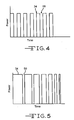
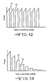
- FIGS 4 to 13 illustrate different controlled power protocols of the present invention.
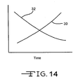
- Figure 14 illustrates the source voltage and the source current during the anodization on-time period.
- the present invention is directed to an anodization protocol for valve metals 14.
- Figure 3a illustrates some of the components used for the anodization protocol.
- the first component is a supply system 10.
- the supply system 10 provides controlled power, a source current and a source voltage.
- the controlled power, the source current and the source voltage are collectively referred to as "output".
- the supply system's 10 output traverses a first electrical conduit 202 to current limiting devices 12A, 12B and 12C.
- Each current limiting device can alter a portion of the supply system's 10 output if the current exceeds a predetermined current level.
- Each current limiting device 12A, 12B and 12C delivers an altered output, which may or may not be altered in relation to the output, through a second electrical conduit 203 to the anode(s) 14 associated with the respective current limiting device 12A, 12B and 12C.
- the anode(s) 14 are submerged in an anodizing electrolyte within a formation tank(s) 16,
- a cathode 18 is positioned in each formation tank 16 and receives a resulting output from the anode and/or the electrolyte.
- the cathode 18 directs the resulting output through a third electrical conduit 204 to the supply system 10.
- This anodization protocol controls the power and current with or without brief interruptions.
- the anodization protocol offers the following advantages over the prior art: 1) controlled power throughout the course of anodizing to decrease and/or avoid excessive heating of the anode; 2) short anodizing time; and 3) smooth change in current and power that avoids disruptive changes in the current and voltage.
- the claimed anodization protocol also results in desired anode electrical properties. Those desired electrical properties include and are not limited to desired DC leakage, a stable shelf life, desired charge/discharge energy efficiency and capacitance, and desired stability during the anode's operating life. These properties are desired for critical applications.
- One such critical application is implantable cardioverter defibrillators.
- the voltage 30 applied to an anode increases with anodizing time, and the current 32 decreases at the same time, as illustrated in Figure 14.
- the power 34 (illustrated in Figures 4 to 13) received by an anode is controlled for a desired power level(s) at specific times:
- the desired power level(s) is designed not to overheat the valve metal 14 (illustrated in Figures 3a and 3b) and simultaneously obtain a desired DC leakage for the anode.
- This output control is smooth and does not interrupt the anodizing process.
- the control is accomplished through electronics that one of ordinary skill in the power fields can manufacture and conforms to the flow chart illustrated in Figure 3b.
- the supply system 10 has a power control unit 100, a voltmeter 200, an ampmeter 240, a multiplier 206, and a difference unit 212.
- the voltmeter 200 measures the output's voltage that traverses the first conduit 202.
- the voltmeter 200 transmits the voltage measurement 208 to the multiplier 206.
- the ampmeter 240 measures the current that traverses the first conduit 202.
- the ampmeter 240 transmits the current measurement 205 to the multiplier 206.
- the multiplier 206 computes the measured power value 210. For example, the multiplier 206 may multiply the current measurement 205 and the voltage measurement 208 to obtain a measured power value 210. The multiplier 206 transmits the measured power value 210 to a difference unit 212.
- the difference unit 212 (which could also be a part of the multiplier 206) also receives a desired power value 214.
- the desired power value 214 can be pre-programmed into the difference unit 212 or alternatively inputted by the user or any third party who desires to input the desired power value 214 for the anode 14.
- the difference unit 212 compares the desired power value 214 to the measured power value 210. If the difference unit 212 calculates that the difference between the desired power value 214 and the measured power value 210 is not zero, the difference unit 212 transmits a first signal 216 to the power control unit 100. In response to the first signal 216, the power control unit 100 adjusts the power control unit's output 202 by adjusting the current and/or the voltage so the difference between the desired power value 214 and the measured power value 210 equals or is adjusted toward zero.
- the difference unit 212 calculates that the difference between the desired power value 214 and the measured power value 210 is zero, the difference unit 212 transmits a second signal 218 to the power control unit 100.
- the second signal 218 instructs the power control unit not to alter the power supply output in conduit 202. It is doubtful the second signal 218 will ever be used since the power supply output in conduit 202 is normally constantly changing to obtain the desired power value. Additionally, the second signal 218 may not even be a transmitted signal.
- the current limiting devices 12A, 12B and 12C receive the output from the electrical conduit 202.
- the current limiting devices are designed to ensure the current that is eventually transmitted to the anodes does not exceed a predetermined value.
- the current limiting devices can be a resistor, a fuse, or any other type of device that can limit the current. If the current limiting device limits the current passing through it or allows the current to pass through it without altering the current, the current limiting device 12A, 12B and 12C transmits what is referred to as the altered output through the second conduit 203.
- the specific limitation of the current varies depending on the desired anode properties.
- the valve metal material 14 receives the altered output from the second conduit 203.
- Each valve metal anode 14 and/or set of anodes 14 is positioned within the formation tank (16).
- the anodizing (formation) electrolyte can be any conventional anodizing electrolyte. Examples of effective anodizing electrolytes are disclosed in commoniy assigned U.S. Patent No. 6,231,993 to Stephenson et al., which is Incorporated herein by reference.
- the electrolyte can be an aqueous solution of ethylene glycol or an aqueous solution of polyethylene glycol and H 3 PO 4 .
- An exemplary formation electrolyte can comprise 10-80 volume percent polyethylene glycol (PEG400) plus 0.1-10 volume percent H 3 PO 4 and de-ionized water having a conductivity of about 10 ⁇ S/cm to about 50,000 ⁇ S/cm at 40°C.
- PEG400 polyethylene glycol
- H 3 PO 4 de-ionized water having a conductivity of about 10 ⁇ S/cm to about 50,000 ⁇ S/cm at 40°C.
- other electrolyte compositions can be used that are designed to obtain desired anode
- the cathode 18 is positioned in each tank 16.
- the cathode 18 returns the resulting output to the supply system 10.
- the resulting output is the current, voltage and power applied to the anode and/or the electrolyte.
- the anodization protocol may incorporate a timing mechanism 98 within a circuitry area 99.
- the circuitry area 99 is the area between and/or including the supply system 10 and the valve metal 14 - but not including the valve metal itself.
- the timing mechanism 98 provides a rest time 50 during the anodization protocol in which the anode 14 is not subject to any controlled power, current or voltage, as illustrated in Figures 4 to 13.
- the rest time 50 can be obtained by the timing mechanism turning on and off a switch, not shown, along the conduit(s) that transports the current, voltage and power to the anodes 14,
- the "on-times" (when the anode 14 receives the desired power, current and voltage) and “off-times” can range from seconds to hours.
- the on-times and off-times can be the same or different, preferably the off-times are shorter than the on-times.
- the on-times and the off-times can be fixed or varied during the course of anodizing.
- the anodes can be anodized continuously. That means the anodizing protocol has no rest or off-time throughout the entire anodization protocol.
- the anodizing methods of the present Invention apply to all valve metals for electrolytic capacitor anodes.
- the valve metal anodes include and are not limited to etched foils, pressed and sintered powder bodies, or other forms of porous structures.
- the anodizing methods of the present invention are particularly useful for anodizing large and high voltage sintered powder anodes. Such anodes are used In tantalum electrolytic capacitors.
- Figures 4 to 13 illustrate some examples of the anodizing protocols of the present invention.
- the x-axis in the figures can be time or voltage.
- the controlled power 34 can also be applied to the anode within the following protocol to obtain the desired decreased DC leakage:
- Constant power 34 anodizing with constant on-times and off-times 50 at a set power value, as illustrated in Figure 4.
- Constant power 34 anodizing with varied on-time and constant off-times 50, as shown in Figure 5.
- Constant power 34 within each pulse varied power between pulses with constant on-times and off-times 50, as exemplified in Figure 6.
- valve metals formed in accordance to the present Invention are for anodes able to handle more than 200 volts without "gray-out” or significant breakdown during anodization, and acceptable anode electrical properties.
- the electrolyte can be agitated during the anodizing.
- the agitation can be created by any conventional agitation device 400.
- Examples of agitation devices 400 include: mechanical stirrers, ultrasonic agitation devices or subsonic agitation devices, and moving the anodes. All of these agitation devices and methods are known to those of ordinary skill in the art.
- the anodization protocol of the present invention was compared to a variation of the anodization protocol described by Stephenson et al. in U.S. Patent No. 6,231,993.
- the valve metal pellets were taken from the same lot of Greatbatch, Inc,'s regular production line and had similar weights - averaged 7.3 grams.
- the electrolyte was 15% PEG400 and 85% water with a sufficient amount of phosphoric acid added to provide a conductivity of 2550 ⁇ S/cm at 40°C. Each pellet was positioned within a formation tank that could contain 300 ml of electrolyte, and were maintained at 40°C.
- the anodes were formed to 240 volts in accordance to the two protocols.
- the prior art anodization protocol took 28.25 hours, and the anode's DC leakage was 0.91 nA/ ⁇ FV.
- the anodization protocol used in this example is referred to as the 17 watt constant power pulse protocol. That protocol has a pulse limited to a maximum power of 17 watts and a maximum current of 1 50 mA. The power-on period was for 50 seconds, and the power-off period was for 10 seconds. No additional rests were taken.
- the resulting anode was formed in 22.8 hours and the anode's DC leakage was 0.92 nA/ ⁇ FV.
Landscapes
- Chemical & Material Sciences (AREA)
- Engineering & Computer Science (AREA)
- Chemical Kinetics & Catalysis (AREA)
- Electrochemistry (AREA)
- Materials Engineering (AREA)
- Metallurgy (AREA)
- Organic Chemistry (AREA)
- Power Engineering (AREA)
- Manufacturing & Machinery (AREA)
- Microelectronics & Electronic Packaging (AREA)
- Electrical Discharge Machining, Electrochemical Machining, And Combined Machining (AREA)
Applications Claiming Priority (1)
| Application Number | Priority Date | Filing Date | Title |
|---|---|---|---|
| US63362404P | 2004-12-06 | 2004-12-06 |
Publications (2)
| Publication Number | Publication Date |
|---|---|
| EP1667178A1 true EP1667178A1 (de) | 2006-06-07 |
| EP1667178B1 EP1667178B1 (de) | 2008-10-08 |
Family
ID=35722394
Family Applications (1)
| Application Number | Title | Priority Date | Filing Date |
|---|---|---|---|
| EP05026466A Expired - Lifetime EP1667178B1 (de) | 2004-12-06 | 2005-12-05 | Verfahren zur Anodisierung von Ventilmetallen mit einer gesteuerten Leistungsversorgung und anodisierte Ventilmetallstruktur |
Country Status (3)
| Country | Link |
|---|---|
| US (1) | US20060191796A1 (de) |
| EP (1) | EP1667178B1 (de) |
| DE (1) | DE602005010191D1 (de) |
Cited By (4)
| Publication number | Priority date | Publication date | Assignee | Title |
|---|---|---|---|---|
| EP1860210A1 (de) * | 2006-05-22 | 2007-11-28 | Siemens Aktiengesellschaft | Verfahren zur elektrolytischen Bearbeitung eines Bauteils |
| WO2018089961A1 (en) * | 2016-11-14 | 2018-05-17 | Avx Corporation | Wet electrolytic capacitor for an implantable medical device |
| WO2018089963A1 (en) * | 2016-11-14 | 2018-05-17 | Avx Corporation | Solid electrolytic capacitor for high voltage environments |
| US10957493B2 (en) | 2017-12-05 | 2021-03-23 | Avx Corporation | Wet electrolytic capacitor for an implantable medical device |
Families Citing this family (12)
| Publication number | Priority date | Publication date | Assignee | Title |
|---|---|---|---|---|
| US20100155645A1 (en) * | 2004-04-01 | 2010-06-24 | Greatbatch Ltd. | Anodizing electrolytes for high voltage capacitor anodes |
| US7952853B2 (en) * | 2004-04-27 | 2011-05-31 | Medtronic, Inc. | Capacitor electrolyte |
| US9548166B2 (en) | 2005-06-30 | 2017-01-17 | Medtronic, Inc. | Capacitor electrolyte |
| US7879217B2 (en) | 2005-12-02 | 2011-02-01 | Greatbatch Ltd. | Method of forming valve metal anode pellets for capacitors using forced convection of liquid electrolyte during anodization |
| CA2661469A1 (en) * | 2008-04-11 | 2009-10-11 | Andre Foucault | Leg rehabilitation apparatus |
| US8605411B2 (en) | 2010-09-16 | 2013-12-10 | Avx Corporation | Abrasive blasted conductive polymer cathode for use in a wet electrolytic capacitor |
| US8514547B2 (en) | 2010-11-01 | 2013-08-20 | Avx Corporation | Volumetrically efficient wet electrolytic capacitor |
| US8259435B2 (en) | 2010-11-01 | 2012-09-04 | Avx Corporation | Hermetically sealed wet electrolytic capacitor |
| US9275799B2 (en) | 2011-12-20 | 2016-03-01 | Avx Corporation | Wet electrolytic capacitor containing an improved anode |
| GB2512481B (en) | 2013-03-15 | 2018-05-30 | Avx Corp | Wet electrolytic capacitor for use at high temperatures |
| GB2512486B (en) | 2013-03-15 | 2018-07-18 | Avx Corp | Wet electrolytic capacitor |
| US11791104B2 (en) * | 2020-05-29 | 2023-10-17 | Pacesetter, Inc. | Reducing variance in capacitor electrodes |
Citations (7)
| Publication number | Priority date | Publication date | Assignee | Title |
|---|---|---|---|---|
| US4026781A (en) * | 1969-08-07 | 1977-05-31 | Scionics Of California Inc. | Anodizing means and techniques |
| US4478689A (en) * | 1981-07-31 | 1984-10-23 | The Boeing Company | Automated alternating polarity direct current pulse electrolytic processing of metals |
| US4517059A (en) * | 1981-07-31 | 1985-05-14 | The Boeing Company | Automated alternating polarity direct current pulse electrolytic processing of metals |
| US4839002A (en) * | 1987-12-23 | 1989-06-13 | International Hardcoat, Inc. | Method and capacitive discharge apparatus for aluminum anodizing |
| US6231993B1 (en) * | 1998-10-01 | 2001-05-15 | Wilson Greatbatch Ltd. | Anodized tantalum pellet for an electrolytic capacitor |
| US20040182717A1 (en) * | 2003-03-17 | 2004-09-23 | Kinard John Tony | Capacitor containing aluminum anode foil anodized in low water content glycerine-phosphate electrolyte without a pre-anodizing hydration step |
| US6802951B2 (en) * | 2002-01-28 | 2004-10-12 | Medtronic, Inc. | Methods of anodizing valve metal anodes |
Family Cites Families (10)
| Publication number | Priority date | Publication date | Assignee | Title |
|---|---|---|---|---|
| US3864219A (en) * | 1974-01-08 | 1975-02-04 | Atomic Energy Commission | Process and electrolyte for applying barrier layer anodic coatings |
| GB8426264D0 (en) * | 1984-10-17 | 1984-11-21 | Alcan Int Ltd | Porous films |
| GB8602582D0 (en) * | 1986-02-03 | 1986-03-12 | Alcan Int Ltd | Porous anodic aluminium oxide films |
| US4936957A (en) * | 1988-03-28 | 1990-06-26 | The United States Of America As Represented By The Secretary Of The Air Force | Thin film oxide dielectric structure and method |
| US4891103A (en) * | 1988-08-23 | 1990-01-02 | Texas Instruments Incorporated | Anadization system with remote voltage sensing and active feedback control capabilities |
| US5185075A (en) * | 1990-10-25 | 1993-02-09 | The Alta Group | Surface treated titanium/titanium alloy articles and process for producing |
| EP0523677A3 (en) * | 1991-07-16 | 1994-10-19 | Canon Kk | Method and apparatus for anodic oxidation treatment |
| US5211832A (en) * | 1992-04-22 | 1993-05-18 | The Alta Group | Process for producing electrically impervious anodized films on valve metals and product thereof |
| AU9652098A (en) * | 1997-11-18 | 1999-06-07 | Mitsubishi Chemical Corporation | Chemical conversion fluid for forming metal oxide film |
| US6777831B2 (en) * | 2000-10-18 | 2004-08-17 | Tecnu, Inc. | Electrochemical processing power device |
-
2005
- 2005-12-01 US US11/164,682 patent/US20060191796A1/en not_active Abandoned
- 2005-12-05 EP EP05026466A patent/EP1667178B1/de not_active Expired - Lifetime
- 2005-12-05 DE DE602005010191T patent/DE602005010191D1/de not_active Expired - Lifetime
Patent Citations (7)
| Publication number | Priority date | Publication date | Assignee | Title |
|---|---|---|---|---|
| US4026781A (en) * | 1969-08-07 | 1977-05-31 | Scionics Of California Inc. | Anodizing means and techniques |
| US4478689A (en) * | 1981-07-31 | 1984-10-23 | The Boeing Company | Automated alternating polarity direct current pulse electrolytic processing of metals |
| US4517059A (en) * | 1981-07-31 | 1985-05-14 | The Boeing Company | Automated alternating polarity direct current pulse electrolytic processing of metals |
| US4839002A (en) * | 1987-12-23 | 1989-06-13 | International Hardcoat, Inc. | Method and capacitive discharge apparatus for aluminum anodizing |
| US6231993B1 (en) * | 1998-10-01 | 2001-05-15 | Wilson Greatbatch Ltd. | Anodized tantalum pellet for an electrolytic capacitor |
| US6802951B2 (en) * | 2002-01-28 | 2004-10-12 | Medtronic, Inc. | Methods of anodizing valve metal anodes |
| US20040182717A1 (en) * | 2003-03-17 | 2004-09-23 | Kinard John Tony | Capacitor containing aluminum anode foil anodized in low water content glycerine-phosphate electrolyte without a pre-anodizing hydration step |
Cited By (7)
| Publication number | Priority date | Publication date | Assignee | Title |
|---|---|---|---|---|
| EP1860210A1 (de) * | 2006-05-22 | 2007-11-28 | Siemens Aktiengesellschaft | Verfahren zur elektrolytischen Bearbeitung eines Bauteils |
| WO2007134917A3 (de) * | 2006-05-22 | 2008-03-20 | Siemens Ag | Verfahren zur elektrolytischen bearbeitung eines bauteils |
| WO2018089961A1 (en) * | 2016-11-14 | 2018-05-17 | Avx Corporation | Wet electrolytic capacitor for an implantable medical device |
| WO2018089963A1 (en) * | 2016-11-14 | 2018-05-17 | Avx Corporation | Solid electrolytic capacitor for high voltage environments |
| US10431389B2 (en) | 2016-11-14 | 2019-10-01 | Avx Corporation | Solid electrolytic capacitor for high voltage environments |
| US10832871B2 (en) | 2016-11-14 | 2020-11-10 | Avx Corporation | Wet electrolytic capacitor for an implantable medical device |
| US10957493B2 (en) | 2017-12-05 | 2021-03-23 | Avx Corporation | Wet electrolytic capacitor for an implantable medical device |
Also Published As
| Publication number | Publication date |
|---|---|
| DE602005010191D1 (de) | 2008-11-20 |
| EP1667178B1 (de) | 2008-10-08 |
| US20060191796A1 (en) | 2006-08-31 |
Similar Documents
| Publication | Publication Date | Title |
|---|---|---|
| US7727372B2 (en) | Anodizing valve metals by self-adjusted current and power | |
| EP1667178B1 (de) | Verfahren zur Anodisierung von Ventilmetallen mit einer gesteuerten Leistungsversorgung und anodisierte Ventilmetallstruktur | |
| US6802951B2 (en) | Methods of anodizing valve metal anodes | |
| US8313621B2 (en) | Valve metal anode pellets for capacitors formed using forced convection of liquid electrolyte during anodization | |
| US6965510B1 (en) | Sintered valve metal powders for implantable capacitors | |
| US6231993B1 (en) | Anodized tantalum pellet for an electrolytic capacitor | |
| US20060091020A1 (en) | Processes and systems for formation of high voltage, anodic oxide on a valve metal anode | |
| US8675348B2 (en) | Capacitor electrolyte | |
| EP1826297A2 (de) | Eloxierung von Elektrolyten unter Verwendung eines zweifachen Säuresystems für Hochspannungselektrolytkondensatoranoden | |
| EP2045367A1 (de) | Verfahren zur anodischen oxidation von aluminiumlegierung und stromversorgung für die anodische oxidation von aluminiumlegierung | |
| US9548166B2 (en) | Capacitor electrolyte | |
| US6334945B1 (en) | Aging process for solid electrode capacitor | |
| CN112267127A (zh) | 一种电解控制电路、消毒液制造装置及电解控制方法 | |
| RU2613250C2 (ru) | Устройство для микродугового оксидирования | |
| KR960010109B1 (ko) | 탄탈 콘덴서의 계단식 화성전압 상승 화성 제조방법 | |
| RU2456697C1 (ru) | Способ получения оксидного слоя на анодах оксидно-полупроводниковых и электролитических конденсаторов | |
| Gladstein et al. | A new method of current density control during the pulse plating process | |
| KR20150141075A (ko) | 다층 접착 코팅을 포함하는 고체 전해 커패시터 | |
| RU2344204C1 (ru) | Способ интенсификации электрохимических процессов | |
| WO2007005914A2 (en) | Capacitor electrolyte | |
| JPH05159981A (ja) | 固体電解コンデンサの製造方法 | |
| JPH05243104A (ja) | 固体電解コンデンサの製造方法 | |
| Debuyck et al. | Correlation between the thickness and the specific mass of an anodization layer on aluminium and the measured current transient |
Legal Events
| Date | Code | Title | Description |
|---|---|---|---|
| PUAI | Public reference made under article 153(3) epc to a published international application that has entered the european phase |
Free format text: ORIGINAL CODE: 0009012 |
|
| AK | Designated contracting states |
Kind code of ref document: A1 Designated state(s): AT BE BG CH CY CZ DE DK EE ES FI FR GB GR HU IE IS IT LI LT LU LV MC NL PL PT RO SE SI SK TR |
|
| AX | Request for extension of the european patent |
Extension state: AL BA HR MK YU |
|
| 17P | Request for examination filed |
Effective date: 20060609 |
|
| 17Q | First examination report despatched |
Effective date: 20060727 |
|
| AKX | Designation fees paid |
Designated state(s): DE FR GB SE |
|
| GRAP | Despatch of communication of intention to grant a patent |
Free format text: ORIGINAL CODE: EPIDOSNIGR1 |
|
| GRAS | Grant fee paid |
Free format text: ORIGINAL CODE: EPIDOSNIGR3 |
|
| GRAA | (expected) grant |
Free format text: ORIGINAL CODE: 0009210 |
|
| AK | Designated contracting states |
Kind code of ref document: B1 Designated state(s): DE FR GB SE |
|
| REG | Reference to a national code |
Ref country code: GB Ref legal event code: FG4D |
|
| RAP2 | Party data changed (patent owner data changed or rights of a patent transferred) |
Owner name: GREATBATCH, INC. |
|
| REF | Corresponds to: |
Ref document number: 602005010191 Country of ref document: DE Date of ref document: 20081120 Kind code of ref document: P |
|
| REG | Reference to a national code |
Ref country code: SE Ref legal event code: TRGR |
|
| RAP2 | Party data changed (patent owner data changed or rights of a patent transferred) |
Owner name: GREATBATCH LTD. |
|
| PLBE | No opposition filed within time limit |
Free format text: ORIGINAL CODE: 0009261 |
|
| STAA | Information on the status of an ep patent application or granted ep patent |
Free format text: STATUS: NO OPPOSITION FILED WITHIN TIME LIMIT |
|
| REG | Reference to a national code |
Ref country code: FR Ref legal event code: TP |
|
| 26N | No opposition filed |
Effective date: 20090709 |
|
| GBPC | Gb: european patent ceased through non-payment of renewal fee |
Effective date: 20091205 |
|
| PG25 | Lapsed in a contracting state [announced via postgrant information from national office to epo] |
Ref country code: GB Free format text: LAPSE BECAUSE OF NON-PAYMENT OF DUE FEES Effective date: 20091205 |
|
| PGFP | Annual fee paid to national office [announced via postgrant information from national office to epo] |
Ref country code: SE Payment date: 20101229 Year of fee payment: 6 |
|
| PGFP | Annual fee paid to national office [announced via postgrant information from national office to epo] |
Ref country code: FR Payment date: 20120104 Year of fee payment: 7 |
|
| REG | Reference to a national code |
Ref country code: SE Ref legal event code: EUG |
|
| PG25 | Lapsed in a contracting state [announced via postgrant information from national office to epo] |
Ref country code: SE Free format text: LAPSE BECAUSE OF NON-PAYMENT OF DUE FEES Effective date: 20111206 |
|
| REG | Reference to a national code |
Ref country code: FR Ref legal event code: ST Effective date: 20130830 |
|
| PG25 | Lapsed in a contracting state [announced via postgrant information from national office to epo] |
Ref country code: FR Free format text: LAPSE BECAUSE OF NON-PAYMENT OF DUE FEES Effective date: 20130102 |
|
| PGFP | Annual fee paid to national office [announced via postgrant information from national office to epo] |
Ref country code: DE Payment date: 20181120 Year of fee payment: 14 |
|
| REG | Reference to a national code |
Ref country code: DE Ref legal event code: R119 Ref document number: 602005010191 Country of ref document: DE |
|
| PG25 | Lapsed in a contracting state [announced via postgrant information from national office to epo] |
Ref country code: DE Free format text: LAPSE BECAUSE OF NON-PAYMENT OF DUE FEES Effective date: 20200701 |