EP1668745B1 - Flexible baugruppe gestapelter chips - Google Patents
Flexible baugruppe gestapelter chips Download PDFInfo
- Publication number
- EP1668745B1 EP1668745B1 EP03770552A EP03770552A EP1668745B1 EP 1668745 B1 EP1668745 B1 EP 1668745B1 EP 03770552 A EP03770552 A EP 03770552A EP 03770552 A EP03770552 A EP 03770552A EP 1668745 B1 EP1668745 B1 EP 1668745B1
- Authority
- EP
- European Patent Office
- Prior art keywords
- chip
- chips
- stacked
- flexible
- folded
- Prior art date
- Legal status (The legal status is an assumption and is not a legal conclusion. Google has not performed a legal analysis and makes no representation as to the accuracy of the status listed.)
- Expired - Lifetime
Links
Images


Classifications
-
- H—ELECTRICITY
- H10—SEMICONDUCTOR DEVICES; ELECTRIC SOLID-STATE DEVICES NOT OTHERWISE PROVIDED FOR
- H10P—GENERIC PROCESSES OR APPARATUS FOR THE MANUFACTURE OR TREATMENT OF DEVICES COVERED BY CLASS H10
- H10P72/00—Handling or holding of wafers, substrates or devices during manufacture or treatment thereof
- H10P72/70—Handling or holding of wafers, substrates or devices during manufacture or treatment thereof for supporting or gripping
- H10P72/74—Handling or holding of wafers, substrates or devices during manufacture or treatment thereof for supporting or gripping using temporarily an auxiliary support
-
- H—ELECTRICITY
- H10—SEMICONDUCTOR DEVICES; ELECTRIC SOLID-STATE DEVICES NOT OTHERWISE PROVIDED FOR
- H10W—GENERIC PACKAGES, INTERCONNECTIONS, CONNECTORS OR OTHER CONSTRUCTIONAL DETAILS OF DEVICES COVERED BY CLASS H10
- H10W70/00—Package substrates; Interposers; Redistribution layers [RDL]
- H10W70/60—Insulating or insulated package substrates; Interposers; Redistribution layers
- H10W70/611—Insulating or insulated package substrates; Interposers; Redistribution layers for connecting multiple chips together
-
- H—ELECTRICITY
- H10—SEMICONDUCTOR DEVICES; ELECTRIC SOLID-STATE DEVICES NOT OTHERWISE PROVIDED FOR
- H10W—GENERIC PACKAGES, INTERCONNECTIONS, CONNECTORS OR OTHER CONSTRUCTIONAL DETAILS OF DEVICES COVERED BY CLASS H10
- H10W70/00—Package substrates; Interposers; Redistribution layers [RDL]
- H10W70/60—Insulating or insulated package substrates; Interposers; Redistribution layers
- H10W70/67—Insulating or insulated package substrates; Interposers; Redistribution layers characterised by their insulating layers or insulating parts
- H10W70/688—Flexible insulating substrates
-
- H—ELECTRICITY
- H10—SEMICONDUCTOR DEVICES; ELECTRIC SOLID-STATE DEVICES NOT OTHERWISE PROVIDED FOR
- H10W—GENERIC PACKAGES, INTERCONNECTIONS, CONNECTORS OR OTHER CONSTRUCTIONAL DETAILS OF DEVICES COVERED BY CLASS H10
- H10W90/00—Package configurations
-
- H—ELECTRICITY
- H10—SEMICONDUCTOR DEVICES; ELECTRIC SOLID-STATE DEVICES NOT OTHERWISE PROVIDED FOR
- H10P—GENERIC PROCESSES OR APPARATUS FOR THE MANUFACTURE OR TREATMENT OF DEVICES COVERED BY CLASS H10
- H10P72/00—Handling or holding of wafers, substrates or devices during manufacture or treatment thereof
- H10P72/70—Handling or holding of wafers, substrates or devices during manufacture or treatment thereof for supporting or gripping
- H10P72/74—Handling or holding of wafers, substrates or devices during manufacture or treatment thereof for supporting or gripping using temporarily an auxiliary support
- H10P72/743—Handling or holding of wafers, substrates or devices during manufacture or treatment thereof for supporting or gripping using temporarily an auxiliary support used as a support during manufacture of interconnect decals or build up layers
-
- H—ELECTRICITY
- H10—SEMICONDUCTOR DEVICES; ELECTRIC SOLID-STATE DEVICES NOT OTHERWISE PROVIDED FOR
- H10P—GENERIC PROCESSES OR APPARATUS FOR THE MANUFACTURE OR TREATMENT OF DEVICES COVERED BY CLASS H10
- H10P72/00—Handling or holding of wafers, substrates or devices during manufacture or treatment thereof
- H10P72/70—Handling or holding of wafers, substrates or devices during manufacture or treatment thereof for supporting or gripping
- H10P72/74—Handling or holding of wafers, substrates or devices during manufacture or treatment thereof for supporting or gripping using temporarily an auxiliary support
- H10P72/7436—Handling or holding of wafers, substrates or devices during manufacture or treatment thereof for supporting or gripping using temporarily an auxiliary support used to support a device or a wafer when forming electrical connections thereto
-
- H—ELECTRICITY
- H10—SEMICONDUCTOR DEVICES; ELECTRIC SOLID-STATE DEVICES NOT OTHERWISE PROVIDED FOR
- H10W—GENERIC PACKAGES, INTERCONNECTIONS, CONNECTORS OR OTHER CONSTRUCTIONAL DETAILS OF DEVICES COVERED BY CLASS H10
- H10W70/00—Package substrates; Interposers; Redistribution layers [RDL]
- H10W70/01—Manufacture or treatment
- H10W70/05—Manufacture or treatment of insulating or insulated package substrates, or of interposers, or of redistribution layers
- H10W70/093—Connecting or disconnecting other interconnections thereto or therefrom, e.g. connecting bond wires or bumps
-
- H—ELECTRICITY
- H10—SEMICONDUCTOR DEVICES; ELECTRIC SOLID-STATE DEVICES NOT OTHERWISE PROVIDED FOR
- H10W—GENERIC PACKAGES, INTERCONNECTIONS, CONNECTORS OR OTHER CONSTRUCTIONAL DETAILS OF DEVICES COVERED BY CLASS H10
- H10W70/00—Package substrates; Interposers; Redistribution layers [RDL]
- H10W70/60—Insulating or insulated package substrates; Interposers; Redistribution layers
-
- H—ELECTRICITY
- H10—SEMICONDUCTOR DEVICES; ELECTRIC SOLID-STATE DEVICES NOT OTHERWISE PROVIDED FOR
- H10W—GENERIC PACKAGES, INTERCONNECTIONS, CONNECTORS OR OTHER CONSTRUCTIONAL DETAILS OF DEVICES COVERED BY CLASS H10
- H10W72/00—Interconnections or connectors in packages
- H10W72/01—Manufacture or treatment
-
- H—ELECTRICITY
- H10—SEMICONDUCTOR DEVICES; ELECTRIC SOLID-STATE DEVICES NOT OTHERWISE PROVIDED FOR
- H10W—GENERIC PACKAGES, INTERCONNECTIONS, CONNECTORS OR OTHER CONSTRUCTIONAL DETAILS OF DEVICES COVERED BY CLASS H10
- H10W72/00—Interconnections or connectors in packages
- H10W72/071—Connecting or disconnecting
- H10W72/075—Connecting or disconnecting of bond wires
- H10W72/07541—Controlling the environment, e.g. atmosphere composition or temperature
- H10W72/07554—Controlling the environment, e.g. atmosphere composition or temperature changes in dispositions
-
- H—ELECTRICITY
- H10—SEMICONDUCTOR DEVICES; ELECTRIC SOLID-STATE DEVICES NOT OTHERWISE PROVIDED FOR
- H10W—GENERIC PACKAGES, INTERCONNECTIONS, CONNECTORS OR OTHER CONSTRUCTIONAL DETAILS OF DEVICES COVERED BY CLASS H10
- H10W72/00—Interconnections or connectors in packages
- H10W72/50—Bond wires
- H10W72/541—Dispositions of bond wires
- H10W72/547—Dispositions of multiple bond wires
-
- H—ELECTRICITY
- H10—SEMICONDUCTOR DEVICES; ELECTRIC SOLID-STATE DEVICES NOT OTHERWISE PROVIDED FOR
- H10W—GENERIC PACKAGES, INTERCONNECTIONS, CONNECTORS OR OTHER CONSTRUCTIONAL DETAILS OF DEVICES COVERED BY CLASS H10
- H10W72/00—Interconnections or connectors in packages
- H10W72/50—Bond wires
- H10W72/59—Bond pads specially adapted therefor
-
- H—ELECTRICITY
- H10—SEMICONDUCTOR DEVICES; ELECTRIC SOLID-STATE DEVICES NOT OTHERWISE PROVIDED FOR
- H10W—GENERIC PACKAGES, INTERCONNECTIONS, CONNECTORS OR OTHER CONSTRUCTIONAL DETAILS OF DEVICES COVERED BY CLASS H10
- H10W72/00—Interconnections or connectors in packages
- H10W72/60—Strap connectors, e.g. thick copper clips for grounding of power devices
-
- H—ELECTRICITY
- H10—SEMICONDUCTOR DEVICES; ELECTRIC SOLID-STATE DEVICES NOT OTHERWISE PROVIDED FOR
- H10W—GENERIC PACKAGES, INTERCONNECTIONS, CONNECTORS OR OTHER CONSTRUCTIONAL DETAILS OF DEVICES COVERED BY CLASS H10
- H10W72/00—Interconnections or connectors in packages
- H10W72/851—Dispositions of multiple connectors or interconnections
- H10W72/853—On the same surface
-
- H—ELECTRICITY
- H10—SEMICONDUCTOR DEVICES; ELECTRIC SOLID-STATE DEVICES NOT OTHERWISE PROVIDED FOR
- H10W—GENERIC PACKAGES, INTERCONNECTIONS, CONNECTORS OR OTHER CONSTRUCTIONAL DETAILS OF DEVICES COVERED BY CLASS H10
- H10W72/00—Interconnections or connectors in packages
- H10W72/851—Dispositions of multiple connectors or interconnections
- H10W72/874—On different surfaces
-
- H—ELECTRICITY
- H10—SEMICONDUCTOR DEVICES; ELECTRIC SOLID-STATE DEVICES NOT OTHERWISE PROVIDED FOR
- H10W—GENERIC PACKAGES, INTERCONNECTIONS, CONNECTORS OR OTHER CONSTRUCTIONAL DETAILS OF DEVICES COVERED BY CLASS H10
- H10W72/00—Interconnections or connectors in packages
- H10W72/90—Bond pads, in general
- H10W72/931—Shapes of bond pads
- H10W72/932—Plan-view shape, i.e. in top view
-
- H—ELECTRICITY
- H10—SEMICONDUCTOR DEVICES; ELECTRIC SOLID-STATE DEVICES NOT OTHERWISE PROVIDED FOR
- H10W—GENERIC PACKAGES, INTERCONNECTIONS, CONNECTORS OR OTHER CONSTRUCTIONAL DETAILS OF DEVICES COVERED BY CLASS H10
- H10W72/00—Interconnections or connectors in packages
- H10W72/90—Bond pads, in general
- H10W72/941—Dispositions of bond pads
- H10W72/9413—Dispositions of bond pads on encapsulations
-
- H—ELECTRICITY
- H10—SEMICONDUCTOR DEVICES; ELECTRIC SOLID-STATE DEVICES NOT OTHERWISE PROVIDED FOR
- H10W—GENERIC PACKAGES, INTERCONNECTIONS, CONNECTORS OR OTHER CONSTRUCTIONAL DETAILS OF DEVICES COVERED BY CLASS H10
- H10W74/00—Encapsulations, e.g. protective coatings
- H10W74/01—Manufacture or treatment
- H10W74/019—Manufacture or treatment using temporary auxiliary substrates
-
- H—ELECTRICITY
- H10—SEMICONDUCTOR DEVICES; ELECTRIC SOLID-STATE DEVICES NOT OTHERWISE PROVIDED FOR
- H10W—GENERIC PACKAGES, INTERCONNECTIONS, CONNECTORS OR OTHER CONSTRUCTIONAL DETAILS OF DEVICES COVERED BY CLASS H10
- H10W90/00—Package configurations
- H10W90/10—Configurations of laterally-adjacent chips
-
- H—ELECTRICITY
- H10—SEMICONDUCTOR DEVICES; ELECTRIC SOLID-STATE DEVICES NOT OTHERWISE PROVIDED FOR
- H10W—GENERIC PACKAGES, INTERCONNECTIONS, CONNECTORS OR OTHER CONSTRUCTIONAL DETAILS OF DEVICES COVERED BY CLASS H10
- H10W90/00—Package configurations
- H10W90/20—Configurations of stacked chips
-
- H—ELECTRICITY
- H10—SEMICONDUCTOR DEVICES; ELECTRIC SOLID-STATE DEVICES NOT OTHERWISE PROVIDED FOR
- H10W—GENERIC PACKAGES, INTERCONNECTIONS, CONNECTORS OR OTHER CONSTRUCTIONAL DETAILS OF DEVICES COVERED BY CLASS H10
- H10W90/00—Package configurations
- H10W90/20—Configurations of stacked chips
- H10W90/288—Configurations of stacked chips characterised by arrangements for thermal management of the stacked chips
-
- H—ELECTRICITY
- H10—SEMICONDUCTOR DEVICES; ELECTRIC SOLID-STATE DEVICES NOT OTHERWISE PROVIDED FOR
- H10W—GENERIC PACKAGES, INTERCONNECTIONS, CONNECTORS OR OTHER CONSTRUCTIONAL DETAILS OF DEVICES COVERED BY CLASS H10
- H10W90/00—Package configurations
- H10W90/701—Package configurations characterised by the relative positions of pads or connectors relative to package parts
- H10W90/751—Package configurations characterised by the relative positions of pads or connectors relative to package parts of bond wires
- H10W90/754—Package configurations characterised by the relative positions of pads or connectors relative to package parts of bond wires between a chip and a stacked insulating package substrate, interposer or RDL
Definitions
- the present invention relates generally to stacking chips and to an improved thermal extraction from the stacked chips structure and, more particularly, to interconnecting chips that electrically form a system-on-a-package (SOP) or which are attached to another SOP, while physically being folded into a three-dimensional arrangement which significantly reduces the footprint of the final assembly.
- SOP system-on-a-package
- NiCr tiecoat significantly improves adhesion retention after plating from neutral potassium gold cyanide bath. Its performance is comparable to samples with chromium tiecoat and better than samples with monel tiecoat. Peel loss after gold plating results from copper undercut, at the copper-polyimide interface, by components of the plating solution.
- Typical stacked die applications require that the chips be thinned to a range of 50 to 125 ⁇ m. This results in special handling requirements as well as special tooling to deal with warpage.
- the typical stacked die arrangements also require high placement accuracy, as one chip is placed upon another which, otherwise, ends up with electrical failures.
- Other problems associated with stacked die applications include excessive epoxy covering bonding pads and special substrate design rules and loop heights for wire bonding have to be applied to prevent shorts.
- the present invention solves these and other problems while still providing many of the same benefits such as reduced space, weight savings and even enhanced performance.
- US 6121676 describes a stacked microelectronic assembly in which conductive terminals are provided at the base of the stack for electrical interconnection by means of solder balls to conductive pads on a circuit board.
- the object of the invention is to provide for an electrically complete system or subsystem consisting of at least two chips folded into a three-dimensional arrangement.
- a three-dimensional flexible package consisting of a plurality of stacked chips, the package including at least two integrated circuit chips where at least one of them provides interconnect pathways for electrical connection to additional chips and at least one chip having additional interconnect wiring to an external package or PCB.
- a flexible structure and a method of interconnecting chips that are folded over into a three-dimensional arrangement that consumes less aerial space when mounted on an external package or PCB.
- a thermally conductive membrane or conduit is folded into the assembly to provide a means for extracting waste heat.
- the three-dimensional extended chip arrangement is attached to a silicon carrier or some other system-on-package (SOP) in order to significantly reduce the amount of SOP real estate utilized by each arrangement and to greatly extend the capabilities of the SOP.
- SOP system-on-package
- the stacked structure does not require excessive thinning of the substrates. Substrates of 200 to 300um thickness can advantageously be used.
- a method of forming a flexible chip stacked chip assembly comprising the steps of: folding a plurality of chips over one another, connecting one chip of said plurality of chips to another by flexible discrete insulated interconnects; and mounting at least one chip on a chip carrier electrically coupled to said plurality of folded chips to provide electrical connection between said plurality of stacked chips to pads on said chip carrier.
- a method of providing a flexible chip stacked chip assembly comprising the steps of: folding a plurality of chips over one another, connecting one chip of said plurality of chips to another by flexible discrete insulated interconnects, wherein the bottommost chip of said plurality of chips is provided with a grid array of solder balls making electrical contact between said plurality of stacked chips to pads on a chip carrier.
- Figure 1 illustrates a cross- sectional view of a temporary carrier 10 upon which a release layer 20 is deposited.
- the purpose of the release layer is to make it possible to attach thereon integrated circuit chips 100, 110, 120 and other constructs associated with the chips, the latter being separated from the temporary carrier at a later step.
- the temporary chip carrier 10 is a transparent substrate such as quartz, boro-silicate or some like type material that can withstand BEOL process temperatures, although other materials can also be used, as it is well known to those skilled in the art.
- Release layer 20 is preferably a spin-on organic insulating layer, such as polyimide. The release process is described in U.S. Patent No.
- Chips 100, 110 and 120 may consist of any structure, device, or module, such as a fully integrated circuit or micro-electromechanical system (MEMS) interconnected to each other or attached to a common module.
- MEMS micro-electromechanical system
- Figure 2 shows the same cross-section of Figure 1 having a dielectric layer 30 with a blanket deposition thereon.
- the dielectric material should preferably be flexible and have good dielectric properties. Examples of such material include polyimide or benzocyclobutene (BCB).
- the purpose of having layer 30 is to physically connect the various chips or modules 100, 110, 120, and to provide a medium for interconnections by way of conductive wires and the like to be formed therein. It also serves as a mechanical support for the final configuration of the assembly.
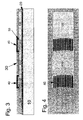
- Figure 3 illustrates the addition of interconnect lines 40 and studs (also referred hereinafter as vias) 50 placed in or on the flexible layer 30.
- the interconnections are preferably made of conductive material such as aluminum or copper, to provide adequate electrical connections between the individual chips 100, 110 and 120.
- the metal lines are preferably scaled to accommodate the necessary signals and power, as required. They are also shaped to provide optimum reliability with regards to the bending required to achieve folding the chips into their final assembly.
- the interconnections are constructed to be 30 ⁇ m wide but only 2 ⁇ m deep or thick. In this manner, they are more likely to bend easily while still having a large cross sectional area. Ideally, they are formed or bent only once during their final assembly.
- Figure 4 is a planar view of Figure 3 . Therein is illustrated in more detail the plurality of parallel interconnects 40 formed within the flexible layer 30, interconnecting the individual chips 100, 110 and 120.
- Figure 5 illustrates a planar view of four chips 100,110, 120 and 130 physically joined by the flexible dielectric layer 30 and electrically connected through the various interconnect wiring 40. Moreover, Figure 5 shows chip 130 being provided with bonding pads 60 that are made available for connecting them to a carrier, package or any other means for providing an electrical connection to the final assembly.
- Figure 6 shows a cross-sectional view how the chips are released from carrier 10 by selectively removing release layer 20 to allow them to be folded over to form the stacked assembly.
- interconnects 40 are determined partially by the order in which the chips are folded.
- interconnects 40 linking chip 100 to chip 110 are, preferably, shorter than the ones linking chips 110 and 120. This is illustrated in Figure 7 showing all three chips in a fully folded arrangement.
- FIG 8 illustrates a similar arrangement to the one shown in Figure 7 .
- a thermally conductive layer or pipeline 300 also referred to thermal sink, which is folded into the stack to provide an efficient means for extracting waste heat generated by the various chips.
- the thermal conductor 300 can be connected to a heat exchanger (not shown) external to the package.
- thermally conductive vias 200 may be incorporated into the interconnect level during the construction of the assembly to allow direct thermal contact between some interior sections of the chips to the thermal sink layer 300.
- Figure 9 is a top-down view of the same structure as shown in Figure 5 after successively folding chips 100 and 120 over 110. Additionally, Figure 9 illustrates how the folded assembly may be wire-bonded to a carrier or package 500. Wire bond pads 60 along the periphery of chip 130 are connected by discrete wires 520 to the package 500 at pads 510, thereby providing the necessary interconnection to the second level package, i.e., silicon substrate 500. Practitioners of the art will recognize that substrate 500 is typically provided with various wiring planes to interconnect all the chips forming the various assemblies. The respective chips 130 of each stacked assembly are provided with their own distinctive footprints, which may vary from one assembly to the next.
- Figure 10 illustrates an even more compact assembly that is made possible when the chip 110 is configured with a ball grid array (BGA) or C4's (Controlled Collapsible Chip Connectors, also referred as 'solder balls') interconnect system 550.
- BGA ball grid array
- C4's Controlled Collapsible Chip Connectors, also referred as 'solder balls' interconnect system 550.
- chip 110 is shown having through connections to the backside for the flexible interconnects.
- Chip 110 may be configured in a conventional manner wherein flexible interconnects are connected on the chip side as the BGA or C4 illustrated in Figure 11 .
- Figure 12 illustrates how the flexible chip arrangements 650 is used to extend the capabilities and reduce the amount aerial space required on a silicon carrier 700 or similar SOP device.
- the SOP device may contain other chips, single or multiple levels of interconnect wiring and passive elements which require large amounts of real estate, such as inductors, transformers and capacitors.
- This invention is used in the field of wireless communications and more particularly, in all phones and the like.
Landscapes
- Structure Of Printed Boards (AREA)
- Cooling Or The Like Of Semiconductors Or Solid State Devices (AREA)
- Battery Mounting, Suspending (AREA)
- Structures For Mounting Electric Components On Printed Circuit Boards (AREA)
- Toys (AREA)
- Wire Bonding (AREA)
Claims (9)
- Flexible Baugruppe gestapelter Chips, welche das Folgende umfasst:mehrere Chips (100, 110, 120), welche zu einem vertikalen Stapel übereinander gefaltet sind und durch diskrete isolierte Zwischenverbindungen (40) flexibel miteinander verbunden sind;gekennzeichnet durcheinen Chip (130), welcher von dem vertikalen Stapel versetzt ist und keinen Teil desselben bildet, auf einem Chipträger (500) angebracht ist, flexibel mit den mehreren gefalteten Chips (100, 110, 120) verbunden ist, und über Drahtverbindungs-Kontaktflecken (60) entlang dem Rand des Chips (150), der durch diskrete Drahtverbindungen (520) an den Kontaktflecken (510) mit dem Chipträger (500) verbunden ist, für eine elektrische Verbindung von den mehreren gestapelten Chips auf dem Chipträger (500) zu Kontaktflecken (510) sorgt.
- Flexible Baugruppe gestapelter Chips nach Anspruch 1, wobei die diskreten isolierten Zwischenverbindungen aus einem leitfähigen Material hergestellt sind, das aus der Gruppe ausgewählt ist, die aus Aluminium und Kupfer besteht.
- Flexible Baugruppe gestapelter Chips nach Anspruch 1, wobei die Länge der Zwischenverbindungen durch die Reihenfolge bestimmt wird, in welcher die Chips gefaltet werden.
- Flexible Baugruppe gestapelter Chips nach Anspruch 1, welche ferner einen Wärmedurchlass umfasst, der in die mehreren gefalteten gestapelten Chips gefaltet ist, um ein Mittel zum Ableiten von überschüssiger Wärme bereitzustellen, die durch die mehreren gefalteten gestapelten Chips erzeugt wird.
- Flexible Baugruppe gestapelter Chips nach Anspruch 4, wobei mindestens ein Chip eine physische Verbindung zu dem Wärmedurchlass herstellt.
- Flexible Baugruppe gestapelter Chips nach Anspruch 1, wobei die Bodenfläche des ersten Chips der mehreren Chips der Bodenfläche des zweiten Chips der Baugruppe gegenüber liegt, während der Boden des dritten Chips der Oberseite des zweiten Chips der Baugruppe gegenüber liegt.
- Flexible Baugruppe gestapelter Chips nach Anspruch 1, wobei die mehreren Chips (100, 110, 120) so angeordnet sind, dass die Chips im Wesentlichen parallel zueinander angeordnet sind.
- Flexible Baugruppe gestapelter Chips nach Anspruch 1, wobei der Chipträger (500) aus der Gruppe ausgewählt ist, die aus einem Siliciumsubstrat, einem System-on-Package, einem Umsetzer und einer Leiterplatte besteht.
- Matrix von Mehr-Chip-Baugruppen, welche mehrere flexible Baugruppen gestapelter Chips umfasst, welche jeweils das Folgende umfassen:mehrere Chips (100, 110, 120), welche zu einem vertikalen Stapel übereinander gefaltet sind und durch diskrete isolierte Zwischenverbindungen flexibel miteinander verbunden sind;gekennzeichnet durcheinen Chip (130), welcher von dem vertikalen Stapel versetzt ist und keinen Teil desselben bildet und flexibel mit den mehreren gefalteten Chips verbunden ist;wobei die Matrix ferner einen Chipträger (700) umfasst, wobei dieser eine Chip (130) auf jeder flexiblen Baugruppe gestapelter Chips jeweils durch Drahtkontaktierung an dem Chipträger angebracht ist.
Applications Claiming Priority (1)
| Application Number | Priority Date | Filing Date | Title |
|---|---|---|---|
| PCT/US2003/030640 WO2005041360A1 (en) | 2003-09-30 | 2003-09-30 | Flexible assembly of stacked chips |
Publications (3)
| Publication Number | Publication Date |
|---|---|
| EP1668745A1 EP1668745A1 (de) | 2006-06-14 |
| EP1668745A4 EP1668745A4 (de) | 2008-12-03 |
| EP1668745B1 true EP1668745B1 (de) | 2011-08-31 |
Family
ID=34519496
Family Applications (1)
| Application Number | Title | Priority Date | Filing Date |
|---|---|---|---|
| EP03770552A Expired - Lifetime EP1668745B1 (de) | 2003-09-30 | 2003-09-30 | Flexible baugruppe gestapelter chips |
Country Status (8)
| Country | Link |
|---|---|
| US (1) | US7355271B2 (de) |
| EP (1) | EP1668745B1 (de) |
| JP (1) | JP4425217B2 (de) |
| CN (1) | CN100448104C (de) |
| AT (1) | ATE522953T1 (de) |
| AU (1) | AU2003279044A1 (de) |
| IL (1) | IL174504A0 (de) |
| WO (1) | WO2005041360A1 (de) |
Families Citing this family (14)
| Publication number | Priority date | Publication date | Assignee | Title |
|---|---|---|---|---|
| US7759167B2 (en) * | 2005-11-23 | 2010-07-20 | Imec | Method for embedding dies |
| KR100726892B1 (ko) | 2006-03-17 | 2007-06-14 | 한국과학기술원 | 3차원 칩 적층 패키지 모듈 및 이의 제조방법 |
| CN101488497B (zh) * | 2007-10-04 | 2012-07-04 | 三星电子株式会社 | 具有可配置垂直输入输出的堆叠半导体装置 |
| US7473618B1 (en) | 2008-04-22 | 2009-01-06 | International Business Machines Corporation | Temporary structure to reduce stress and warpage in a flip chip organic package |
| WO2013087101A1 (en) * | 2011-12-14 | 2013-06-20 | Reinhardt Microtech Gmbh | Substrate-supported circuit parts with free-standing three-dimensional structures |
| WO2014105725A1 (en) * | 2012-12-28 | 2014-07-03 | Volcano Corporation | Intravascular ultrasound imaging apparatus, interface architecture, and method of manufacturing |
| US20140224882A1 (en) * | 2013-02-14 | 2014-08-14 | Douglas R. Hackler, Sr. | Flexible Smart Card Transponder |
| CN103523739A (zh) * | 2013-11-05 | 2014-01-22 | 华进半导体封装先导技术研发中心有限公司 | 环境mems传感器三维柔性基板封装结构及制作方法 |
| CN104465548A (zh) * | 2014-12-10 | 2015-03-25 | 华进半导体封装先导技术研发中心有限公司 | 一种三维柔性封装结构及其注塑成型方法 |
| US9984962B2 (en) * | 2015-08-31 | 2018-05-29 | Arizona Board Of Regents On Behalf Of Arizona State University | Systems and methods for hybrid flexible electronics with rigid integrated circuits |
| KR102497583B1 (ko) | 2015-10-27 | 2023-02-10 | 삼성전자주식회사 | 유연한 연결부를 갖는 반도체 장치 및 그 제조방법 |
| EP3206229B1 (de) | 2016-02-09 | 2020-10-07 | AT & S Austria Technologie & Systemtechnik Aktiengesellschaft | Verfahren zur herstellung von flexiblen elektronischen vorrichtungen |
| CN113161338B (zh) * | 2021-03-30 | 2025-06-13 | 广东汇芯半导体有限公司 | 智能功率模块和智能功率模块的制备方法 |
| CN115565890B (zh) * | 2022-12-07 | 2023-04-18 | 西北工业大学 | 一种折叠式多芯片柔性集成封装方法及柔性集成封装芯片 |
Citations (1)
| Publication number | Priority date | Publication date | Assignee | Title |
|---|---|---|---|---|
| US6121676A (en) * | 1996-12-13 | 2000-09-19 | Tessera, Inc. | Stacked microelectronic assembly and method therefor |
Family Cites Families (22)
| Publication number | Priority date | Publication date | Assignee | Title |
|---|---|---|---|---|
| JP2985484B2 (ja) * | 1992-03-19 | 1999-11-29 | 株式会社日立製作所 | 半導体装置とその製造方法 |
| US4933810A (en) * | 1987-04-30 | 1990-06-12 | Honeywell Inc. | Integrated circuit interconnector |
| US5028983A (en) * | 1988-10-28 | 1991-07-02 | International Business Machines Corporation | Multilevel integrated circuit packaging structures |
| US5239448A (en) * | 1991-10-28 | 1993-08-24 | International Business Machines Corporation | Formulation of multichip modules |
| US5198965A (en) * | 1991-12-18 | 1993-03-30 | International Business Machines Corporation | Free form packaging of specific functions within a computer system |
| FR2704690B1 (fr) * | 1993-04-27 | 1995-06-23 | Thomson Csf | Procédé d'encapsulation de pastilles semi-conductrices, dispositif obtenu par ce procédé et application à l'interconnexion de pastilles en trois dimensions. |
| JP3611957B2 (ja) * | 1997-10-29 | 2005-01-19 | 日東電工株式会社 | 積層型実装体 |
| JPH11249215A (ja) * | 1998-03-06 | 1999-09-17 | Olympus Optical Co Ltd | フレキシブルプリント配線基板を有するカメラ |
| JP2000088921A (ja) * | 1998-09-08 | 2000-03-31 | Sony Corp | 半導体装置 |
| JP3879803B2 (ja) * | 1999-03-25 | 2007-02-14 | セイコーエプソン株式会社 | 半導体装置及びその製造方法、回路基板並びに電子機器 |
| JP2001085608A (ja) * | 1999-09-17 | 2001-03-30 | Sony Corp | 半導体装置 |
| US6572387B2 (en) * | 1999-09-24 | 2003-06-03 | Staktek Group, L.P. | Flexible circuit connector for stacked chip module |
| KR100530911B1 (ko) * | 1999-10-01 | 2005-11-23 | 세이코 엡슨 가부시키가이샤 | 배선 기판, 반도체 장치 및 그 제조, 검사 및 실장 방법,회로 기판 및 전자 기기 |
| JP3721893B2 (ja) * | 1999-10-20 | 2005-11-30 | セイコーエプソン株式会社 | 半導体装置、ならびに電子機器 |
| JP4135284B2 (ja) * | 1999-12-07 | 2008-08-20 | ソニー株式会社 | 半導体モジュールおよび電子回路装置 |
| JP3855594B2 (ja) * | 2000-04-25 | 2006-12-13 | セイコーエプソン株式会社 | 半導体装置 |
| JP2002009229A (ja) * | 2000-06-20 | 2002-01-11 | Seiko Epson Corp | 半導体装置 |
| JP2002009230A (ja) * | 2000-06-20 | 2002-01-11 | Seiko Epson Corp | 半導体装置 |
| JP2002270759A (ja) * | 2001-03-14 | 2002-09-20 | Matsushita Electric Ind Co Ltd | 半導体チップ及びマルチチップモジュール |
| JP4633971B2 (ja) * | 2001-07-11 | 2011-02-16 | ルネサスエレクトロニクス株式会社 | 半導体装置 |
| JP2003133518A (ja) * | 2001-10-29 | 2003-05-09 | Mitsubishi Electric Corp | 半導体モジュール |
| US7071547B2 (en) * | 2002-09-11 | 2006-07-04 | Tessera, Inc. | Assemblies having stacked semiconductor chips and methods of making same |
-
2003
- 2003-09-30 AU AU2003279044A patent/AU2003279044A1/en not_active Abandoned
- 2003-09-30 US US10/573,561 patent/US7355271B2/en not_active Expired - Lifetime
- 2003-09-30 CN CNB038271508A patent/CN100448104C/zh not_active Expired - Lifetime
- 2003-09-30 WO PCT/US2003/030640 patent/WO2005041360A1/en not_active Ceased
- 2003-09-30 AT AT03770552T patent/ATE522953T1/de not_active IP Right Cessation
- 2003-09-30 JP JP2005509922A patent/JP4425217B2/ja not_active Expired - Lifetime
- 2003-09-30 EP EP03770552A patent/EP1668745B1/de not_active Expired - Lifetime
-
2006
- 2006-03-23 IL IL174504A patent/IL174504A0/en unknown
Patent Citations (1)
| Publication number | Priority date | Publication date | Assignee | Title |
|---|---|---|---|---|
| US6121676A (en) * | 1996-12-13 | 2000-09-19 | Tessera, Inc. | Stacked microelectronic assembly and method therefor |
Also Published As
| Publication number | Publication date |
|---|---|
| JP2007521636A (ja) | 2007-08-02 |
| US7355271B2 (en) | 2008-04-08 |
| US20070059951A1 (en) | 2007-03-15 |
| ATE522953T1 (de) | 2011-09-15 |
| WO2005041360A1 (en) | 2005-05-06 |
| IL174504A0 (en) | 2006-08-01 |
| JP4425217B2 (ja) | 2010-03-03 |
| CN1839518A (zh) | 2006-09-27 |
| EP1668745A4 (de) | 2008-12-03 |
| CN100448104C (zh) | 2008-12-31 |
| AU2003279044A1 (en) | 2005-05-11 |
| EP1668745A1 (de) | 2006-06-14 |
Similar Documents
| Publication | Publication Date | Title |
|---|---|---|
| US6365962B1 (en) | Flip-chip on flex for high performance packaging applications | |
| US11309304B2 (en) | Stackable electronic package and method of fabricating same | |
| US5703400A (en) | Fabrication and structures of two-sided molded circuit modules with flexible interconnect layers | |
| JP3217045B2 (ja) | 集積回路チップ・キャリア・アセンブリおよび形成方法 | |
| US5373627A (en) | Method of forming multi-chip module with high density interconnections | |
| US7669320B2 (en) | Coreless cavity substrates for chip packaging and their fabrication | |
| KR101690549B1 (ko) | 내장 칩 패키지 | |
| US7397117B2 (en) | Chip package with die and substrate | |
| US6835598B2 (en) | Stacked semiconductor module and method of manufacturing the same | |
| KR101653856B1 (ko) | 반도체 장치 및 그 제조방법 | |
| TWI647790B (zh) | 以聚合物部件爲主的互連體 | |
| EP1668745B1 (de) | Flexible baugruppe gestapelter chips | |
| KR101486722B1 (ko) | 단일층 코어리스 기판 | |
| KR20020055573A (ko) | 기판 상에서의 수직 어셈블리를 위해 폴딩된 상호접속기상에 적층된 칩-스케일 패키지 | |
| WO2007109492A2 (en) | Low profile semiconductor package-on-package | |
| US9299647B2 (en) | Electrical interconnect for an integrated circuit package and method of making same | |
| US9917073B2 (en) | Reconstituted wafer-level package dram with conductive interconnects formed in encapsulant at periphery of the package | |
| US20080036063A1 (en) | Semiconductor package having flexible lead connection plate for electrically connecting base and chip | |
| CN112599499A (zh) | 天线封装结构及封装方法 | |
| US20100127407A1 (en) | Two-sided substrateless multichip module and method of manufacturing same | |
| KR100877320B1 (ko) | 가요성 적층형 칩 어셈블리 | |
| US7785928B2 (en) | Integrated circuit device and method of manufacturing thereof |
Legal Events
| Date | Code | Title | Description |
|---|---|---|---|
| PUAI | Public reference made under article 153(3) epc to a published international application that has entered the european phase |
Free format text: ORIGINAL CODE: 0009012 |
|
| 17P | Request for examination filed |
Effective date: 20060407 |
|
| AK | Designated contracting states |
Kind code of ref document: A1 Designated state(s): AT BE BG CH CY CZ DE DK EE ES FI FR GB GR HU IE IT LI LU MC NL PT RO SE SI SK TR |
|
| DAX | Request for extension of the european patent (deleted) | ||
| A4 | Supplementary search report drawn up and despatched |
Effective date: 20081104 |
|
| 17Q | First examination report despatched |
Effective date: 20101018 |
|
| GRAP | Despatch of communication of intention to grant a patent |
Free format text: ORIGINAL CODE: EPIDOSNIGR1 |
|
| GRAS | Grant fee paid |
Free format text: ORIGINAL CODE: EPIDOSNIGR3 |
|
| GRAA | (expected) grant |
Free format text: ORIGINAL CODE: 0009210 |
|
| AK | Designated contracting states |
Kind code of ref document: B1 Designated state(s): AT BE BG CH CY CZ DE DK EE ES FI FR GB GR HU IE IT LI LU MC NL PT RO SE SI SK TR |
|
| REG | Reference to a national code |
Ref country code: CH Ref legal event code: NV Representative=s name: IBM RESEARCH GMBH ZURICH RESEARCH LABORATORY INTEL Ref country code: GB Ref legal event code: FG4D Ref country code: CH Ref legal event code: EP |
|
| REG | Reference to a national code |
Ref country code: IE Ref legal event code: FG4D |
|
| REG | Reference to a national code |
Ref country code: GB Ref legal event code: 746 Effective date: 20111004 |
|
| REG | Reference to a national code |
Ref country code: DE Ref legal event code: R096 Ref document number: 60338287 Country of ref document: DE Effective date: 20111110 |
|
| REG | Reference to a national code |
Ref country code: DE Ref legal event code: R084 Ref document number: 60338287 Country of ref document: DE Effective date: 20110922 |
|
| REG | Reference to a national code |
Ref country code: NL Ref legal event code: VDEP Effective date: 20110831 |
|
| PG25 | Lapsed in a contracting state [announced via postgrant information from national office to epo] |
Ref country code: FI Free format text: LAPSE BECAUSE OF FAILURE TO SUBMIT A TRANSLATION OF THE DESCRIPTION OR TO PAY THE FEE WITHIN THE PRESCRIBED TIME-LIMIT Effective date: 20110831 Ref country code: NL Free format text: LAPSE BECAUSE OF FAILURE TO SUBMIT A TRANSLATION OF THE DESCRIPTION OR TO PAY THE FEE WITHIN THE PRESCRIBED TIME-LIMIT Effective date: 20110831 Ref country code: SE Free format text: LAPSE BECAUSE OF FAILURE TO SUBMIT A TRANSLATION OF THE DESCRIPTION OR TO PAY THE FEE WITHIN THE PRESCRIBED TIME-LIMIT Effective date: 20110831 |
|
| REG | Reference to a national code |
Ref country code: AT Ref legal event code: MK05 Ref document number: 522953 Country of ref document: AT Kind code of ref document: T Effective date: 20110831 |
|
| PG25 | Lapsed in a contracting state [announced via postgrant information from national office to epo] |
Ref country code: SI Free format text: LAPSE BECAUSE OF FAILURE TO SUBMIT A TRANSLATION OF THE DESCRIPTION OR TO PAY THE FEE WITHIN THE PRESCRIBED TIME-LIMIT Effective date: 20110831 Ref country code: GR Free format text: LAPSE BECAUSE OF FAILURE TO SUBMIT A TRANSLATION OF THE DESCRIPTION OR TO PAY THE FEE WITHIN THE PRESCRIBED TIME-LIMIT Effective date: 20111201 Ref country code: AT Free format text: LAPSE BECAUSE OF FAILURE TO SUBMIT A TRANSLATION OF THE DESCRIPTION OR TO PAY THE FEE WITHIN THE PRESCRIBED TIME-LIMIT Effective date: 20110831 Ref country code: CY Free format text: LAPSE BECAUSE OF FAILURE TO SUBMIT A TRANSLATION OF THE DESCRIPTION OR TO PAY THE FEE WITHIN THE PRESCRIBED TIME-LIMIT Effective date: 20110831 |
|
| PG25 | Lapsed in a contracting state [announced via postgrant information from national office to epo] |
Ref country code: BE Free format text: LAPSE BECAUSE OF FAILURE TO SUBMIT A TRANSLATION OF THE DESCRIPTION OR TO PAY THE FEE WITHIN THE PRESCRIBED TIME-LIMIT Effective date: 20110831 |
|
| PG25 | Lapsed in a contracting state [announced via postgrant information from national office to epo] |
Ref country code: CZ Free format text: LAPSE BECAUSE OF FAILURE TO SUBMIT A TRANSLATION OF THE DESCRIPTION OR TO PAY THE FEE WITHIN THE PRESCRIBED TIME-LIMIT Effective date: 20110831 Ref country code: SK Free format text: LAPSE BECAUSE OF FAILURE TO SUBMIT A TRANSLATION OF THE DESCRIPTION OR TO PAY THE FEE WITHIN THE PRESCRIBED TIME-LIMIT Effective date: 20110831 Ref country code: MC Free format text: LAPSE BECAUSE OF NON-PAYMENT OF DUE FEES Effective date: 20110930 |
|
| REG | Reference to a national code |
Ref country code: CH Ref legal event code: PL |
|
| PG25 | Lapsed in a contracting state [announced via postgrant information from national office to epo] |
Ref country code: EE Free format text: LAPSE BECAUSE OF FAILURE TO SUBMIT A TRANSLATION OF THE DESCRIPTION OR TO PAY THE FEE WITHIN THE PRESCRIBED TIME-LIMIT Effective date: 20110831 Ref country code: IT Free format text: LAPSE BECAUSE OF FAILURE TO SUBMIT A TRANSLATION OF THE DESCRIPTION OR TO PAY THE FEE WITHIN THE PRESCRIBED TIME-LIMIT Effective date: 20110831 Ref country code: RO Free format text: LAPSE BECAUSE OF FAILURE TO SUBMIT A TRANSLATION OF THE DESCRIPTION OR TO PAY THE FEE WITHIN THE PRESCRIBED TIME-LIMIT Effective date: 20110831 |
|
| PG25 | Lapsed in a contracting state [announced via postgrant information from national office to epo] |
Ref country code: DK Free format text: LAPSE BECAUSE OF FAILURE TO SUBMIT A TRANSLATION OF THE DESCRIPTION OR TO PAY THE FEE WITHIN THE PRESCRIBED TIME-LIMIT Effective date: 20110831 |
|
| REG | Reference to a national code |
Ref country code: IE Ref legal event code: MM4A |
|
| PLBE | No opposition filed within time limit |
Free format text: ORIGINAL CODE: 0009261 |
|
| STAA | Information on the status of an ep patent application or granted ep patent |
Free format text: STATUS: NO OPPOSITION FILED WITHIN TIME LIMIT |
|
| PG25 | Lapsed in a contracting state [announced via postgrant information from national office to epo] |
Ref country code: LI Free format text: LAPSE BECAUSE OF NON-PAYMENT OF DUE FEES Effective date: 20110930 Ref country code: CH Free format text: LAPSE BECAUSE OF NON-PAYMENT OF DUE FEES Effective date: 20110930 Ref country code: IE Free format text: LAPSE BECAUSE OF NON-PAYMENT OF DUE FEES Effective date: 20110930 |
|
| 26N | No opposition filed |
Effective date: 20120601 |
|
| REG | Reference to a national code |
Ref country code: DE Ref legal event code: R097 Ref document number: 60338287 Country of ref document: DE Effective date: 20120601 |
|
| PGFP | Annual fee paid to national office [announced via postgrant information from national office to epo] |
Ref country code: FR Payment date: 20121001 Year of fee payment: 10 |
|
| PG25 | Lapsed in a contracting state [announced via postgrant information from national office to epo] |
Ref country code: ES Free format text: LAPSE BECAUSE OF FAILURE TO SUBMIT A TRANSLATION OF THE DESCRIPTION OR TO PAY THE FEE WITHIN THE PRESCRIBED TIME-LIMIT Effective date: 20111211 |
|
| PG25 | Lapsed in a contracting state [announced via postgrant information from national office to epo] |
Ref country code: LU Free format text: LAPSE BECAUSE OF NON-PAYMENT OF DUE FEES Effective date: 20110930 |
|
| PG25 | Lapsed in a contracting state [announced via postgrant information from national office to epo] |
Ref country code: BG Free format text: LAPSE BECAUSE OF FAILURE TO SUBMIT A TRANSLATION OF THE DESCRIPTION OR TO PAY THE FEE WITHIN THE PRESCRIBED TIME-LIMIT Effective date: 20111130 |
|
| PG25 | Lapsed in a contracting state [announced via postgrant information from national office to epo] |
Ref country code: TR Free format text: LAPSE BECAUSE OF FAILURE TO SUBMIT A TRANSLATION OF THE DESCRIPTION OR TO PAY THE FEE WITHIN THE PRESCRIBED TIME-LIMIT Effective date: 20110831 |
|
| PG25 | Lapsed in a contracting state [announced via postgrant information from national office to epo] |
Ref country code: HU Free format text: LAPSE BECAUSE OF FAILURE TO SUBMIT A TRANSLATION OF THE DESCRIPTION OR TO PAY THE FEE WITHIN THE PRESCRIBED TIME-LIMIT Effective date: 20110831 |
|
| REG | Reference to a national code |
Ref country code: FR Ref legal event code: ST Effective date: 20140530 |
|
| PG25 | Lapsed in a contracting state [announced via postgrant information from national office to epo] |
Ref country code: PT Free format text: LAPSE BECAUSE OF FAILURE TO SUBMIT A TRANSLATION OF THE DESCRIPTION OR TO PAY THE FEE WITHIN THE PRESCRIBED TIME-LIMIT Effective date: 20110831 |
|
| PG25 | Lapsed in a contracting state [announced via postgrant information from national office to epo] |
Ref country code: FR Free format text: LAPSE BECAUSE OF NON-PAYMENT OF DUE FEES Effective date: 20130930 |
|
| REG | Reference to a national code |
Ref country code: DE Ref legal event code: R082 Ref document number: 60338287 Country of ref document: DE Representative=s name: KUISMA, SIRPA, FI |
|
| PGFP | Annual fee paid to national office [announced via postgrant information from national office to epo] |
Ref country code: GB Payment date: 20220919 Year of fee payment: 20 Ref country code: DE Payment date: 20220831 Year of fee payment: 20 |
|
| P01 | Opt-out of the competence of the unified patent court (upc) registered |
Effective date: 20230423 |
|
| REG | Reference to a national code |
Ref country code: DE Ref legal event code: R071 Ref document number: 60338287 Country of ref document: DE |
|
| REG | Reference to a national code |
Ref country code: GB Ref legal event code: PE20 Expiry date: 20230929 |
|
| PG25 | Lapsed in a contracting state [announced via postgrant information from national office to epo] |
Ref country code: GB Free format text: LAPSE BECAUSE OF EXPIRATION OF PROTECTION Effective date: 20230929 |