EP1669748A1 - Biomolekülnachweiselement und verfahren zur nukleinsäureanalyse damit - Google Patents
Biomolekülnachweiselement und verfahren zur nukleinsäureanalyse damit Download PDFInfo
- Publication number
- EP1669748A1 EP1669748A1 EP04772319A EP04772319A EP1669748A1 EP 1669748 A1 EP1669748 A1 EP 1669748A1 EP 04772319 A EP04772319 A EP 04772319A EP 04772319 A EP04772319 A EP 04772319A EP 1669748 A1 EP1669748 A1 EP 1669748A1
- Authority
- EP
- European Patent Office
- Prior art keywords
- probe
- immobilized
- biomolecule detecting
- detecting element
- electrode
- Prior art date
- Legal status (The legal status is an assumption and is not a legal conclusion. Google has not performed a legal analysis and makes no representation as to the accuracy of the status listed.)
- Withdrawn
Links
Images


Classifications
-
- C—CHEMISTRY; METALLURGY
- C12—BIOCHEMISTRY; BEER; SPIRITS; WINE; VINEGAR; MICROBIOLOGY; ENZYMOLOGY; MUTATION OR GENETIC ENGINEERING
- C12Q—MEASURING OR TESTING PROCESSES INVOLVING ENZYMES, NUCLEIC ACIDS OR MICROORGANISMS; COMPOSITIONS OR TEST PAPERS THEREFOR; PROCESSES OF PREPARING SUCH COMPOSITIONS; CONDITION-RESPONSIVE CONTROL IN MICROBIOLOGICAL OR ENZYMOLOGICAL PROCESSES
- C12Q1/00—Measuring or testing processes involving enzymes, nucleic acids or microorganisms; Compositions therefor; Processes of preparing such compositions
- C12Q1/68—Measuring or testing processes involving enzymes, nucleic acids or microorganisms; Compositions therefor; Processes of preparing such compositions involving nucleic acids
- C12Q1/6813—Hybridisation assays
- C12Q1/6834—Enzymatic or biochemical coupling of nucleic acids to a solid phase
- C12Q1/6837—Enzymatic or biochemical coupling of nucleic acids to a solid phase using probe arrays or probe chips
-
- G—PHYSICS
- G01—MEASURING; TESTING
- G01N—INVESTIGATING OR ANALYSING MATERIALS BY DETERMINING THEIR CHEMICAL OR PHYSICAL PROPERTIES
- G01N27/00—Investigating or analysing materials by the use of electric, electrochemical, or magnetic means
- G01N27/26—Investigating or analysing materials by the use of electric, electrochemical, or magnetic means by investigating electrochemical variables; by using electrolysis or electrophoresis
- G01N27/403—Cells and electrode assemblies
- G01N27/414—Ion-sensitive or chemical field-effect transistors, i.e. ISFETS or CHEMFETS
- G01N27/4145—Ion-sensitive or chemical field-effect transistors, i.e. ISFETS or CHEMFETS specially adapted for biomolecules, e.g. gate electrode with immobilised receptors
-
- B—PERFORMING OPERATIONS; TRANSPORTING
- B01—PHYSICAL OR CHEMICAL PROCESSES OR APPARATUS IN GENERAL
- B01J—CHEMICAL OR PHYSICAL PROCESSES, e.g. CATALYSIS OR COLLOID CHEMISTRY; THEIR RELEVANT APPARATUS
- B01J2219/00—Chemical, physical or physico-chemical processes in general; Their relevant apparatus
- B01J2219/00274—Sequential or parallel reactions; Apparatus and devices for combinatorial chemistry or for making arrays; Chemical library technology
- B01J2219/00277—Apparatus
- B01J2219/00497—Features relating to the solid phase supports
- B01J2219/00527—Sheets
- B01J2219/00529—DNA chips
-
- B—PERFORMING OPERATIONS; TRANSPORTING
- B01—PHYSICAL OR CHEMICAL PROCESSES OR APPARATUS IN GENERAL
- B01J—CHEMICAL OR PHYSICAL PROCESSES, e.g. CATALYSIS OR COLLOID CHEMISTRY; THEIR RELEVANT APPARATUS
- B01J2219/00—Chemical, physical or physico-chemical processes in general; Their relevant apparatus
- B01J2219/00274—Sequential or parallel reactions; Apparatus and devices for combinatorial chemistry or for making arrays; Chemical library technology
- B01J2219/00583—Features relative to the processes being carried out
- B01J2219/00603—Making arrays on substantially continuous surfaces
- B01J2219/00605—Making arrays on substantially continuous surfaces the compounds being directly bound or immobilised to solid supports
- B01J2219/00608—DNA chips
-
- B—PERFORMING OPERATIONS; TRANSPORTING
- B01—PHYSICAL OR CHEMICAL PROCESSES OR APPARATUS IN GENERAL
- B01J—CHEMICAL OR PHYSICAL PROCESSES, e.g. CATALYSIS OR COLLOID CHEMISTRY; THEIR RELEVANT APPARATUS
- B01J2219/00—Chemical, physical or physico-chemical processes in general; Their relevant apparatus
- B01J2219/00274—Sequential or parallel reactions; Apparatus and devices for combinatorial chemistry or for making arrays; Chemical library technology
- B01J2219/00583—Features relative to the processes being carried out
- B01J2219/00603—Making arrays on substantially continuous surfaces
- B01J2219/00605—Making arrays on substantially continuous surfaces the compounds being directly bound or immobilised to solid supports
- B01J2219/00612—Making arrays on substantially continuous surfaces the compounds being directly bound or immobilised to solid supports the surface being inorganic
-
- B—PERFORMING OPERATIONS; TRANSPORTING
- B01—PHYSICAL OR CHEMICAL PROCESSES OR APPARATUS IN GENERAL
- B01J—CHEMICAL OR PHYSICAL PROCESSES, e.g. CATALYSIS OR COLLOID CHEMISTRY; THEIR RELEVANT APPARATUS
- B01J2219/00—Chemical, physical or physico-chemical processes in general; Their relevant apparatus
- B01J2219/00274—Sequential or parallel reactions; Apparatus and devices for combinatorial chemistry or for making arrays; Chemical library technology
- B01J2219/00583—Features relative to the processes being carried out
- B01J2219/00603—Making arrays on substantially continuous surfaces
- B01J2219/00605—Making arrays on substantially continuous surfaces the compounds being directly bound or immobilised to solid supports
- B01J2219/00623—Immobilisation or binding
- B01J2219/00626—Covalent
-
- B—PERFORMING OPERATIONS; TRANSPORTING
- B01—PHYSICAL OR CHEMICAL PROCESSES OR APPARATUS IN GENERAL
- B01J—CHEMICAL OR PHYSICAL PROCESSES, e.g. CATALYSIS OR COLLOID CHEMISTRY; THEIR RELEVANT APPARATUS
- B01J2219/00—Chemical, physical or physico-chemical processes in general; Their relevant apparatus
- B01J2219/00274—Sequential or parallel reactions; Apparatus and devices for combinatorial chemistry or for making arrays; Chemical library technology
- B01J2219/00583—Features relative to the processes being carried out
- B01J2219/00603—Making arrays on substantially continuous surfaces
- B01J2219/00605—Making arrays on substantially continuous surfaces the compounds being directly bound or immobilised to solid supports
- B01J2219/00632—Introduction of reactive groups to the surface
- B01J2219/00637—Introduction of reactive groups to the surface by coating it with another layer
-
- B—PERFORMING OPERATIONS; TRANSPORTING
- B01—PHYSICAL OR CHEMICAL PROCESSES OR APPARATUS IN GENERAL
- B01J—CHEMICAL OR PHYSICAL PROCESSES, e.g. CATALYSIS OR COLLOID CHEMISTRY; THEIR RELEVANT APPARATUS
- B01J2219/00—Chemical, physical or physico-chemical processes in general; Their relevant apparatus
- B01J2219/00274—Sequential or parallel reactions; Apparatus and devices for combinatorial chemistry or for making arrays; Chemical library technology
- B01J2219/00583—Features relative to the processes being carried out
- B01J2219/00603—Making arrays on substantially continuous surfaces
- B01J2219/00653—Making arrays on substantially continuous surfaces the compounds being bound to electrodes embedded in or on the solid supports
Definitions
- the present invention relates to biotechnology, particularly technologies in the field of genetic examination, such as genetic diagnosis, DNA sequencing analysis, and gene polymorphism analysis.
- the invention relates to a biomolecule detecting element suitable for accurately analyzing a plurality of different nucleic acids in parallel, and to a method for analyzing nucleic acids employing the element.
- a redox marker is used in combination.
- Clinical Micro Sensors Inc. has developed a system in which one end of a molecule called a molecular wire is immobilized on a metal electrode, and a DNA probe is bound to the other end. Transfer of electrons between the redox marker and the metal electrode based on the hybridization with a target gene is detected in the form of a current change, thereby detecting the target gene (Nature Biotechnology, vol. 16, (1998), p.27 and p.40).
- Non-patent Document 1 Nature Biotechnology, vol. 16, (1998), p.27 and p.40
- the aforementioned electrochemical detection method does not require expensive lasers or complex optical systems, systems can be reduced in size and cost as compared with systems based on the fluorescent detection method.
- this method is based on a redox reaction on a metal electrode as a basic detection principle, if an oxidizing substance or a reducing substance (such as ascorbic acid) exists in the sample, a current based on oxidation or reduction flows, which would hinder the gene detection and the detection accuracy would deteriorate.
- the measurement of current is associated with the progress of electrode reaction on the metal electrode. Because such an electrode reaction is irreversible and constitutes a nonequilibrium reaction, corrosion of the electrode develops and gases are generated, for example. As a result, the stability of current measurement is adversely affected and the detection accuracy deteriorates particularly when measurement is repeated.
- a probe comprising a living body-related substance, such as nucleic acid, is immobilized on the surface of a metal that is electrically connected to the gate of a field effect transistor, and then a complex with a target substance is formed on the metal surface when a change in surface charge density is detected using a field effect.
- an intercalator is introduced or the complex is combined with a charged particle, such as an ion, so that the amount of change in surface charge density can be increased and the change in surface charge potential can be detected with a large S/N ratio.
- wireless communications technologies have made a significant progress in recent years, and a wireless communications chip has been developed in which a tag that is equivalent to a barcode is integrated.
- individual wireless communications chips can be identified, and their use as a distribution management chip is being considered.
- a tagged wireless communications chip is used as a DNA chip, it must be of low-power consumption because electric power is fed wirelessly.
- the voltage measurement system which consumes less power than the current measurement system, is therefore suitable for the wireless communications-based DNA chip.
- the invention provides a biomolecule detecting element comprising:
- the probe-immobilized electrode extends from immediately above the gate electrode along the film surface of the insulating film to the region where the biomolecular probe is immobilized, wherein the connection wire is connected to the probe-immobilized electrode immediately above the gate electrode.
- the probe-immobilized electrode is disposed away from immediately above the gate electrode, and the connection wire is disposed within the insulating film along the film surface.
- the biomolecular probe may comprise a nucleic acid, polynucleotide, or synthetic oligonucleotide.
- the biomolecular probe has one end thereof immobilized on the surface of the probe-immobilized electrode and specifically binds to and/or reacts with a living body-related substance in a sample.
- the biomolecular probe may be comprised of a single-strand probe, and detection sensitivity with respect to a specific binding between the probe and a complementary strand can be enhanced by placing an intercalator at the double-stranded portion formed by the specific binding.
- the probe-immobilized electrode may be comprised of one or a combination of materials including gold, platinum, palladium, titanium, chromium, aluminum, polysilicon, tantalum, or molybdenum.
- a transmission/reception antenna may be formed in the insulating film.
- the invention also provides a biomolecule detecting element comprising:
- the invention also provides a method for analyzing nucleic acids using the biomolecule detecting element of the invention, comprising the steps of:
- the invention further provides a method for analyzing nucleic acids using the biomolecule detecting element of the invention, comprising the steps of:
- the biomolecule detecting element of the invention does not require expensive lasers or complex optical detection systems. Because the biomolecule detecting element of the invention is based on the detection of surface potentials in a steady state, as opposed to the current detection-based (amperometric) system, there is no problem of instability in signal values due to the corrosion of substrates or the development of gas, or the interference by oxidizing and/or reducing substances. Thus, detection of biological material can be made highly accurately and stably.
- DNA is used as an example of a biomolecule.
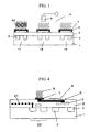
- Fig. 1 schematically shows a cross section of a biomolecule detecting element (biomolecule detecting transistor) according to the invention.
- An insulated gate field effect transistor is produced by forming a gate insulating film 2, a source 3, and a drain 4 on the surface of a silicon substrate 1, and providing a gate electrode 5 on the gate insulating film between the source and drain.
- On the surface of the gate electrode 5 is further formed an insulating film, such that the gate electrode 5 is embedded in the insulating film 2.
- a throughhole is formed in the insulating film 2, and a lead-out electrode 6 is formed using a conductive material and is placed in an electrical contact with the gate electrode 5.
- a floating electrode 7 is further formed on the surface of the gate insulating film and is placed in electrical contact with the lead-out electrode 6.
- a DNA probe 8 is immobilized on the surface of the floating electrode 7. The thus produced gene transistor is immersed in a sample solution 10 together with a reference electrode 9 when in use.
- the gate insulating film is comprised of silicon oxide (SiO 2 ), silicon nitride (SiN), aluminum oxide (Al 2 O 3 ), or tantalum oxide (Ta 2 O 5 ), either individually or in combination.
- silicon nitride (SiN), aluminum oxide (Al 2 O 3 ), or tantalum oxide (Ta 2 O 5 ) is layered on the silicon oxide (SiO 2 ), thereby producing a double-layered structure.
- the material of the gate electrode 5 is preferably polysilicon because it provides good compatibility with the so-called self-align process, in which the source and drain are formed through the injection of ions via a polysilicon gate.
- the lead-out electrode 6 is used as part of wiring and is therefore preferably made of a material with low resistance and good etching processibility, for example. Examples include polysilicon, aluminum, and molybdenum.
- the floating electrode 7, which comes into direct contact with a sample solution, is preferably made of a material that is highly chemically stable and that exhibits a stable potential, and which has high affinity to biological materials to which the floating electrode is fixed. Examples include noble metals such as gold, platinum, silver, and palladium.
- the lead-out electrode and the floating electrode can be formed of the same material, such as gold, by using a pattern forming method for the floating electrode, such as the liftoff method.
- the need for fixing the DNA probe 8 on the channel between the source and drain of the transistor is eliminated, so that the DNA probe 8 can be formed on any desired location on the chip by extending the floating electrode 7 or the lead-out electrode 6, as shown in Fig. 1.
- the region where the DNA probe 8, which comes into contact with the sample solution, for example, is formed and the transistor region where electronic circuits are formed can be laid out separately on the chip, which enables highly reliable measurement.
- biomolecule detecting chips are larger in size than the conventional semiconductor chips, and biomolecule detecting chips have even been developed that are as large as a slide glass (26 mm x 76 mm). While it is preferable to design the biomolecule detecting transistor of the invention to be of a small size of approximately 5 mm squares for price reduction purposes, the concept of the invention may be applied to chips whose size is about the size of a slide glass.
- the DNA probe (biomolecular probe) 8 is normally comprised of not more than 300 bases, using fragments of oligonucleotide or cDNA. When oligonucleotide is used, the nucleic acid fragment is preferably not more than 80 bases long.
- one end of the DNA probe is chemically modified with an amino group (NH 2 group), a thiol group (SH group), or biotin, for example.
- the surface of the gate electrode is chemically modified with aminopropylethoxysilane or polylysine, for example, thereby introducing an amino group on the gate surface.
- a DNA probe chemically modified with an amino group through a reaction with glutaraldehyde or phenylenediisocyanate (PDC) is then immobilized on the gate surface.
- PDC glutaraldehyde or phenylenediisocyanate
- gold is used for the gate electrode, and the DNA probe is immobilized using the affinity between the thiol group and gold.
- streptavidin is introduced on the gate electrode surface, and the DNA probe is immobilized on the gate surface using the affinity between the biotin and streptavidin.
- a solution containing the DNA probe is added dropwise or spotted onto the floating electrode surface alone.
- a reference electrode 9 is disposed that provides a reference for potential measurement.
- the reference electrode is normally prepared by immersing a silver/silver chloride electrode or a photosensitive electrode in an internal solution of a predetermined composition and concentration. Because the operating point is adjusted by changing the electric characteristics of the biomolecule detecting transistor, a predetermined voltage can be applied to the reference electrode 9.
- the target gene and the DNA probe hybridize under proper reaction conditions and form a complex.
- DNA is charged negatively. Therefore, the formation of a complex by hybridization leads to a change in charge density near the gate of the FET, which causes a change in the gate surface potential. This change produces an action equivalent to a gate voltage change in the FET, whereby the channel conductivity changes.
- the formation of the complex namely the presence of the target gene, can be detected via the change in drain current through the source 3 and the drain 4.
- Biomolecule detecting transistor of the present embodiment Gene analysis is performed using the biomolecule detecting transistor of the present embodiment in accordance with the following procedure, for example.
- the biomolecule detecting transistor of the invention and 0.5 ml of buffer solution are put in a reaction vessel, and transistor signals are measured. Thereafter, gene analysis is performed in the following steps (a) to (e).
- steps (b) and (d) may be skipped.
- Fig. 2 schematically shows a gene examination system in which the biomolecule detecting transistor according to the first embodiment is used.
- a reference transistor 12 is used in addition to the biomolecule detecting transistor 11 shown in Fig. 1, and a differential measurement is carried out using the two transistors.
- a DNA probe 8 having a base sequence complementary to that of the target gene in the sample is immobilized on the surface of the gate of the reference transistor.
- a DNA probe 13 having a base sequence different from the complementary base sequence of the target gene is immobilized on the surface of the gate of the reference transistor.
- a reference electrode 9 as a reference for potential measurement is provided to stably measure the surface potential of the biomolecule detecting transistor and the reference transistor. The surface potential of the biomolecule detecting transistor and that of the reference transistor are measured by a drive circuit 14, and a measurement signal is fed to a signal processing circuit 16 via a differential measuring circuit 15.
- the biomolecule detecting transistor and the reference transistor should desirably have identical electric characteristics. Therefore, a pair of transistors integrated on the same substrate are preferably used.
- the reference transistor may be commonly used. In this case, the different biomolecule detecting transistors and the common reference transistor are used for a differential measurement.
- Fig. 3 schematically shows a cross section of another example of a measurement system employing the biomolecule detecting transistor shown in Fig. 1.
- three FETs are integrated.
- a first biomolecule detecting transistor 17 is used for detecting a first target gene.
- a second transistor 18 is used for detecting a second target gene.
- a third transistor 19 is used as the reference transistor.
- a DNA probe having a base sequence complementary to that of the first and the second gene, respectively is immobilized.
- On the surface of the gate electrode of the reference FET a DNA probe having a base sequence different from the complementary base sequence of the first or second gene is immobilized.
- the state shown in Fig. 3 is that where a sample solution containing only the first gene has been introduced into the aforementioned integrated transistors and hybridized to the target gene, and then an intercalator has been added.
- the first gene hybridizes to the DNA probe of the first biomolecule detecting transistor 17 alone, thereby forming a double strand.
- the intercalator 20 reacts with and binds to the double-stranded DNA alone, without binding to single-strand DNA. Because the intercalator has a charge, the surface charge density of the first biomolecule detecting transistor 17 alone changes, resulting in a change in its output signal.
- the surface charge density of the second biomolecule detecting transistor 18 and that of the reference transistor 19 do not change, so that there is no change in their output signals.
- the output signal of the former alone changes, whereby the first target gene can be detected.
- the intercalator ethidium bromide, Hoechst 33258, or PicoGreen, for example, may be used.
- Alcohol dehydrogenase-related genes are known to have single nucleotide polymorphisms (SNPs).
- SNPs single nucleotide polymorphisms
- a first and a second DNA probe of 17-bases long each consisting of 8 bases in front and 8 bases after an SNP site were synthesized.
- the base sequences are as follows:
- human genome was extracted from the white blood cells in blood, and a 100-base length region including the aforementioned SNP site was amplified. Thereafter, the region was introduced into the first and second biomolecule detecting transistors and the reference transistor, and then hybridization was carried out at 45°C for 8 hours. After hybridization, washing was carried out using a buffer solution so as to remove unreacted sample, followed by the introduction of intercalator. For measurement, a buffer solution was introduced into the first and second biomolecule detecting transistors and the reference transistor, and the output voltage of each transistor, a differential output between the first biomolecule detecting transistor and the reference transistor, and a differential output between the second biomolecule detecting transistor and the reference transistor were measured. Thereafter, the sample was introduced, followed by hybridization and washing.
- Hoechst 33258 was then introduced as the intercalator, and the output voltage of each transistor, a differential output between the first biomolecule detecting transistor and the reference transistor, and a differential output between the second biomolecule detecting transistor and the reference transistor were measured. In this way, changes in output voltage before and after the introduction of the sample and intercalator were measured.
- the differential output between the first biomolecule detecting transistor and the reference transistor after the introduction of the sample solution and after the introduction of intercalator was 15.0 mV and -12.0 mV, respectively. Because DNA is negatively charged in the solution, the output of an n-channel FET is shifted in the positive direction. On the other hand, because the intercalator is positively charged in the solution, the output of the FET is shifted in the negative direction.
- the differential output between the second biomolecule detecting transistor and the reference transistor was 1.5 mV and
- the differential output between the first biomolecule detecting transistor and the reference transistor after the introduction of the sample solution and after the introduction of intercalator was 2.3 mV and 0.7 mV, respectively.
- the differential output between the second biomolecule detecting transistor and the reference transistor was 11.0 mV and -8.0 mV, respectively, thus also indicating a significant difference.
- the differential output between the first biomolecule detecting transistor and the reference transistor after the introduction of the sample solution and after the introduction of intercalator was 6.5 mV and -4.8 mV, respectively.
- the differential output between the second biomolecule detecting transistor and the reference transistor was 5.5 mV and -4.5 mV, respectively, thus indicating an almost one to one ratio.
- Figs. 4 and 5 schematically show another example of the biomolecule detecting transistor according to the invention.
- the biomolecule detecting transistor is equivalent to the biomolecule detecting transistor shown in Fig. 3 to which a transmission/reception antenna 21 has been added in the gate insulating film 2.
- the antenna 21, which may be formed simultaneously with the formation of the gate electrode 5, is connected to an element 22 of a transmission/reception circuit embedded in chip.
- a reference electrode 9 is comprised of Ti on which Pt is stacked and is directly formed on a substrate.
- a lead-out electrode 6 is embedded in an insulating film 2 and extended therein, and a floating electrode 7 is formed at the end thereof.
- Fig. 5 shows a plan view of the embodiment.
- Source 3 and drain 4 of the transistor, DNA probes 8 and 13, and antenna 21 can be separately laid out on the chip. The only portions exposed on the chip surface are the floating electrode 7, DNA probes 8 and 13, and insulating film 2, and the transistor portion and the antenna portion are protected by the insulating film 2.
- a signal measured by the biomolecule detecting transistor can be transmitted via the antenna to an external receiver for signal processing.
- the antenna is embedded in the insulating film 2, it does not come into direct contact with the sample solution, so that the antenna is not subject to corrosion due to solutions or characteristics changes due to the adsorption of proteins.
- the biomolecule detecting transistor can be suitably used for highly reliable measurement.
- Fig. 6 shows an example in which the biomolecule detecting transistor of the present embodiment and a chip having a wireless communications function are integrated.
- a source 3 and a drain 4 of the biomolecule detecting transistor are formed, and a floating electrode 7 and the gate are connected via a lead-out electrode 6.
- a DNA probe 8 is immobilized on the floating electrode.
- an antenna 21, a computation circuit 23, a memory circuit 24, a reception circuit 25, a transmission circuit 26, and a power supply circuit 27 have been integrated. If a target DNA with a complementary sequence exists in a sample, it hybridizes to the DNA probe on the floating electrode 7, forming a double strand. The formation of the double strand is detected by a field effect transistor.
- the memory circuit 24 are stored ID information distinguishing one chip substrate from another, DNA probe sequence information, and coding protein information, for example. These information, as well as the information regarding the result of hybridization reaction, are transmitted to an outside reception device via the antenna and transmission circuit. Electromagnetic wave transmitted from outside the chip is received by the antenna and converted through the reception circuit and the power supply circuit into sufficient power that can be used by the chip. The power is then fed to the individual elements including the field effect transistor, transmission circuit, and memory circuit for their operation.
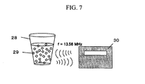
- the biomolecule detecting transistor 29 of the invention and 0.5 ml of a buffer solution are put in a reaction vessel 28, and transistor signals are measured.
- the measured signals are transmitted to an external receiver, and then a gene analysis is carried out in accordance with the following steps (a) to (f):
- the difference in output values of the biomolecule detecting transistor obtained by the above-described two measurements constitutes the signal from the double-stranded DNA formed by hybridization.
- electromagnetic wave of 13.56MHz is used, for example, between the transistor and an externally located transmission/reception apparatus 30.
- the type of DNA existing in the sample, its shape, and its sequence can be analyzed.
- the present chip employs wireless communications technology for transmission/reception and for the supply of power, the chip can be directly put in a sample for measurement without requiring any wiring between the chip and external circuitry.
- a simple measurement system can be constructed.
- the washing steps (b) and (d) may be omitted and the entire measurement sequence can be completed with the biomolecule detecting transistor immersed in the sample solution.
Landscapes
- Chemical & Material Sciences (AREA)
- Life Sciences & Earth Sciences (AREA)
- Health & Medical Sciences (AREA)
- Molecular Biology (AREA)
- Organic Chemistry (AREA)
- Engineering & Computer Science (AREA)
- Physics & Mathematics (AREA)
- Immunology (AREA)
- Proteomics, Peptides & Aminoacids (AREA)
- Zoology (AREA)
- Analytical Chemistry (AREA)
- Biochemistry (AREA)
- General Health & Medical Sciences (AREA)
- Wood Science & Technology (AREA)
- Biotechnology (AREA)
- General Physics & Mathematics (AREA)
- Biophysics (AREA)
- Microelectronics & Electronic Packaging (AREA)
- Chemical Kinetics & Catalysis (AREA)
- Microbiology (AREA)
- Spectroscopy & Molecular Physics (AREA)
- Pathology (AREA)
- Electrochemistry (AREA)
- Bioinformatics & Cheminformatics (AREA)
- General Engineering & Computer Science (AREA)
- Genetics & Genomics (AREA)
- Apparatus Associated With Microorganisms And Enzymes (AREA)
- Investigating Or Analyzing Materials By The Use Of Electric Means (AREA)
- Measuring Or Testing Involving Enzymes Or Micro-Organisms (AREA)
Applications Claiming Priority (2)
| Application Number | Priority Date | Filing Date | Title |
|---|---|---|---|
| JP2003306906A JP2005077210A (ja) | 2003-08-29 | 2003-08-29 | 生体分子検出素子及びそれを用いた核酸解析方法 |
| PCT/JP2004/012363 WO2005022142A1 (ja) | 2003-08-29 | 2004-08-27 | 生体分子検出素子及びそれを用いた核酸解析方法 |
Publications (2)
| Publication Number | Publication Date |
|---|---|
| EP1669748A1 true EP1669748A1 (de) | 2006-06-14 |
| EP1669748A4 EP1669748A4 (de) | 2008-12-17 |
Family
ID=34269409
Family Applications (1)
| Application Number | Title | Priority Date | Filing Date |
|---|---|---|---|
| EP04772319A Withdrawn EP1669748A4 (de) | 2003-08-29 | 2004-08-27 | Biomolekülnachweiselement und verfahren zur nukleinsäureanalyse damit |
Country Status (5)
| Country | Link |
|---|---|
| US (1) | US20060141474A1 (de) |
| EP (1) | EP1669748A4 (de) |
| JP (1) | JP2005077210A (de) |
| CN (2) | CN100447563C (de) |
| WO (1) | WO2005022142A1 (de) |
Cited By (5)
| Publication number | Priority date | Publication date | Assignee | Title |
|---|---|---|---|---|
| EP1850124A3 (de) * | 2006-04-26 | 2009-01-21 | Samsung Electronics Co., Ltd. | Feldeffekttransistor zur Detektion von ionischem Material und Verfahren zur Detektion von ionischem Material unter Verwendung desselben |
| US8128796B2 (en) * | 2007-06-22 | 2012-03-06 | Hitachi, Limited | Analyzer |
| WO2016025743A1 (en) * | 2014-08-14 | 2016-02-18 | Regents Of The University Of Minnesota | Electrolyte-gated transistors for detection of molecules |
| EP3387420A4 (de) * | 2015-12-09 | 2019-08-14 | Ramot at Tel-Aviv University Ltd. | Erfassungsverfahren und -system |
| EP4134667A1 (de) * | 2006-12-14 | 2023-02-15 | Life Technologies Corporation | Vorrichtungen zur messung von analyten unter verwendung von fet-arrays |
Families Citing this family (86)
| Publication number | Priority date | Publication date | Assignee | Title |
|---|---|---|---|---|
| US7692219B1 (en) | 2004-06-25 | 2010-04-06 | University Of Hawaii | Ultrasensitive biosensors |
| JP3874772B2 (ja) * | 2004-07-21 | 2007-01-31 | 株式会社日立製作所 | 生体関連物質測定装置及び測定方法 |
| KR100737860B1 (ko) * | 2005-01-07 | 2007-07-12 | 삼성전자주식회사 | 무선 안테나를 이용한 바이오결합 검출장치 및 그 방법 |
| CN101180641B (zh) * | 2005-01-31 | 2012-02-08 | 株式会社半导体能源研究所 | 半导体器件及其制造方法 |
| EP1856741A4 (de) * | 2005-03-08 | 2010-04-21 | Ca Nat Research Council | Elektrostatisch geregelte elektroleitfähigkeits-einrichtung auf atomarem massstab |
| JP4631027B2 (ja) * | 2005-03-29 | 2011-02-16 | 独立行政法人産業技術総合研究所 | Icタグ搭載型バイオセンサーおよびその包装体 |
| JP4081477B2 (ja) * | 2005-03-29 | 2008-04-23 | 株式会社日立製作所 | 生体分子検出装置及びそれを用いた生体分子検出方法 |
| US20070292855A1 (en) * | 2005-08-19 | 2007-12-20 | Intel Corporation | Method and CMOS-based device to analyze molecules and nanomaterials based on the electrical readout of specific binding events on functionalized electrodes |
| JP4353958B2 (ja) | 2005-09-15 | 2009-10-28 | 株式会社日立製作所 | Dna計測装置、及びdna計測方法 |
| JP4173503B2 (ja) | 2005-10-19 | 2008-10-29 | 株式会社日立製作所 | Rfidシステムおよびrfidシステムの処理方法 |
| GB2432217A (en) * | 2005-11-09 | 2007-05-16 | Seiko Epson Corp | Application of biosensor chips |
| KR100718144B1 (ko) | 2006-01-09 | 2007-05-14 | 삼성전자주식회사 | 이온 물질 검출용 fet 기반 센서, 그를 포함하는 이온물질 검출 장치 및 그를 이용한 이온 물질 검출 방법 |
| JP4735833B2 (ja) * | 2006-01-13 | 2011-07-27 | セイコーエプソン株式会社 | バイオチップ及びバイオセンサ |
| JP4331181B2 (ja) * | 2006-03-30 | 2009-09-16 | 株式会社日立製作所 | 測定装置及び分析用素子 |
| KR101195612B1 (ko) * | 2006-04-10 | 2012-10-29 | 삼성전자주식회사 | 금층을 포함하는 전계 효과 트랜지스터, 상기 전계 효과 트랜지스터를 포함하는 미세유동장치, 및 상기 전계 효과 트랜지스터 및 미세유동장치를 이용하여 티올기를 포함하는 분석물을 검출하는 방법 |
| JP4936536B2 (ja) * | 2006-07-13 | 2012-05-23 | 国立大学法人富山大学 | 定量・定性分析方法 |
| US20080108164A1 (en) * | 2006-11-06 | 2008-05-08 | Oleynik Vladislav A | Sensor System and Method |
| JP4751302B2 (ja) * | 2006-11-21 | 2011-08-17 | 株式会社日立製作所 | 電位差式センサ及び分析用素子 |
| US8349167B2 (en) | 2006-12-14 | 2013-01-08 | Life Technologies Corporation | Methods and apparatus for detecting molecular interactions using FET arrays |
| US8262900B2 (en) | 2006-12-14 | 2012-09-11 | Life Technologies Corporation | Methods and apparatus for measuring analytes using large scale FET arrays |
| US11339430B2 (en) | 2007-07-10 | 2022-05-24 | Life Technologies Corporation | Methods and apparatus for measuring analytes using large scale FET arrays |
| JP4512607B2 (ja) | 2007-03-22 | 2010-07-28 | 信越化学工業株式会社 | マイクロアレイ作製用基板の製造方法 |
| JP4850854B2 (ja) | 2007-03-22 | 2012-01-11 | 信越化学工業株式会社 | マイクロアレイ作製用基板の製造方法 |
| KR100923048B1 (ko) | 2007-06-11 | 2009-10-22 | 김성천 | 미지의 생체분자와 단일가닥핵산의 결합 프로파일을생성하기 위한 핵산칩, 핵산칩의 제조방법, 및 핵산칩을이용한 미지의 생체분자 분석방법 |
| US8198658B2 (en) * | 2007-06-13 | 2012-06-12 | Samsung Electronics Co., Ltd. | Device and method for detecting biomolecules using adsorptive medium and field effect transistor |
| KR101465961B1 (ko) * | 2007-10-09 | 2014-12-01 | 삼성전자주식회사 | 유전자 검출 방법 및 장치 |
| JP4731544B2 (ja) * | 2007-12-17 | 2011-07-27 | 株式会社日立製作所 | 生体分子検出装置及びそれを用いた生体分子検出方法 |
| EP2307577B1 (de) | 2008-06-25 | 2015-06-03 | Life Technologies Corporation | Verfahren zur analytmessung mithilfe grosser fet-arrays |
| TWI351435B (en) * | 2008-06-30 | 2011-11-01 | Univ Nat Yunlin Sci & Tech | Separative extended gate field effect transistor b |
| KR101026468B1 (ko) | 2008-09-10 | 2011-04-01 | 한국전자통신연구원 | 생분자 검출 장치 및 검출 방법 |
| US20100301398A1 (en) | 2009-05-29 | 2010-12-02 | Ion Torrent Systems Incorporated | Methods and apparatus for measuring analytes |
| CN103901090B (zh) * | 2008-10-22 | 2017-03-22 | 生命技术公司 | 用于生物和化学分析的集成式传感器阵列 |
| US20100137143A1 (en) | 2008-10-22 | 2010-06-03 | Ion Torrent Systems Incorporated | Methods and apparatus for measuring analytes |
| WO2010132263A2 (en) * | 2009-05-15 | 2010-11-18 | University Of Florida Research Foundation Inc. | Wireless based marine pathogens detection system |
| US8776573B2 (en) | 2009-05-29 | 2014-07-15 | Life Technologies Corporation | Methods and apparatus for measuring analytes |
| US20120261274A1 (en) | 2009-05-29 | 2012-10-18 | Life Technologies Corporation | Methods and apparatus for measuring analytes |
| US8673627B2 (en) | 2009-05-29 | 2014-03-18 | Life Technologies Corporation | Apparatus and methods for performing electrochemical reactions |
| WO2010142773A2 (en) * | 2009-06-10 | 2010-12-16 | Helmholtz Zentrum München Deutsches Forschungszentrum Für Gesundheit Und Umwelt (Gmbh) | Semiconductor biosensors |
| KR101711205B1 (ko) | 2009-12-21 | 2017-03-02 | 삼성전자주식회사 | 전계효과 트랜지스터 및 이에 기반한 센서 |
| EP2588851B1 (de) | 2010-06-30 | 2016-12-21 | Life Technologies Corporation | Ion-sensing charge-accumulation circuit and method |
| TWI465716B (zh) | 2010-06-30 | 2014-12-21 | 生命技術公司 | 用於檢測及測量化學反應及化合物之電晶體電路 |
| EP2588850B1 (de) | 2010-06-30 | 2016-12-28 | Life Technologies Corporation | Trockentestverfahren für isfet-arrays |
| US11307166B2 (en) | 2010-07-01 | 2022-04-19 | Life Technologies Corporation | Column ADC |
| US8653567B2 (en) | 2010-07-03 | 2014-02-18 | Life Technologies Corporation | Chemically sensitive sensor with lightly doped drains |
| CN101915799A (zh) * | 2010-07-15 | 2010-12-15 | 长沙理工大学 | 一种用于dna分子检测的延长栅场效应晶体管传感芯片 |
| WO2012036679A1 (en) | 2010-09-15 | 2012-03-22 | Life Technologies Corporation | Methods and apparatus for measuring analytes |
| JP5920687B2 (ja) * | 2010-09-17 | 2016-05-18 | 国立大学法人 東京大学 | Dna塩基配列解析装置およびdna塩基配列解析方法 |
| US8685324B2 (en) | 2010-09-24 | 2014-04-01 | Life Technologies Corporation | Matched pair transistor circuits |
| US8450131B2 (en) | 2011-01-11 | 2013-05-28 | Nanohmics, Inc. | Imprinted semiconductor multiplex detection array |
| EP2700937A4 (de) | 2011-04-20 | 2014-09-03 | Nat Univ Corp Tokyo Med & Dent | Elektrodenchip zum nachweis biologischer moleküle und verfahren zum nachweis biologischer moleküle |
| US9970984B2 (en) | 2011-12-01 | 2018-05-15 | Life Technologies Corporation | Method and apparatus for identifying defects in a chemical sensor array |
| US8821798B2 (en) | 2012-01-19 | 2014-09-02 | Life Technologies Corporation | Titanium nitride as sensing layer for microwell structure |
| US8747748B2 (en) | 2012-01-19 | 2014-06-10 | Life Technologies Corporation | Chemical sensor with conductive cup-shaped sensor surface |
| US8786331B2 (en) | 2012-05-29 | 2014-07-22 | Life Technologies Corporation | System for reducing noise in a chemical sensor array |
| US9080968B2 (en) | 2013-01-04 | 2015-07-14 | Life Technologies Corporation | Methods and systems for point of use removal of sacrificial material |
| US9841398B2 (en) | 2013-01-08 | 2017-12-12 | Life Technologies Corporation | Methods for manufacturing well structures for low-noise chemical sensors |
| US8962366B2 (en) | 2013-01-28 | 2015-02-24 | Life Technologies Corporation | Self-aligned well structures for low-noise chemical sensors |
| US8841217B1 (en) | 2013-03-13 | 2014-09-23 | Life Technologies Corporation | Chemical sensor with protruded sensor surface |
| US8963216B2 (en) | 2013-03-13 | 2015-02-24 | Life Technologies Corporation | Chemical sensor with sidewall spacer sensor surface |
| US9116117B2 (en) | 2013-03-15 | 2015-08-25 | Life Technologies Corporation | Chemical sensor with sidewall sensor surface |
| WO2014149779A1 (en) | 2013-03-15 | 2014-09-25 | Life Technologies Corporation | Chemical device with thin conductive element |
| EP2972279B1 (de) | 2013-03-15 | 2021-10-06 | Life Technologies Corporation | Chemischer sensor mit stetigen sensoroberflächen |
| CN105264366B (zh) | 2013-03-15 | 2019-04-16 | 生命科技公司 | 具有一致传感器表面区域的化学传感器 |
| US9835585B2 (en) | 2013-03-15 | 2017-12-05 | Life Technologies Corporation | Chemical sensor with protruded sensor surface |
| US20140336063A1 (en) | 2013-05-09 | 2014-11-13 | Life Technologies Corporation | Windowed Sequencing |
| US10458942B2 (en) | 2013-06-10 | 2019-10-29 | Life Technologies Corporation | Chemical sensor array having multiple sensors per well |
| JP6154011B2 (ja) * | 2013-06-27 | 2017-06-28 | 株式会社日立製作所 | 半導体装置およびその製造方法 |
| US20160054312A1 (en) | 2014-04-28 | 2016-02-25 | Nanomedical Diagnostics, Inc. | Chemically differentiated sensor array |
| CN104485334B (zh) * | 2014-12-16 | 2018-02-13 | 京东方科技集团股份有限公司 | 阵列基板及其制作方法、显示装置 |
| US12298301B2 (en) | 2014-12-18 | 2025-05-13 | Cardea Bio, Inc. | Chemically-sensitive field effect transistors, systems, and methods for manufacturing and using the same |
| US10006910B2 (en) | 2014-12-18 | 2018-06-26 | Agilome, Inc. | Chemically-sensitive field effect transistors, systems, and methods for manufacturing and using the same |
| US9618474B2 (en) | 2014-12-18 | 2017-04-11 | Edico Genome, Inc. | Graphene FET devices, systems, and methods of using the same for sequencing nucleic acids |
| KR102593647B1 (ko) | 2014-12-18 | 2023-10-26 | 라이프 테크놀로지스 코포레이션 | 트랜스미터 구성을 갖춘 높은 데이터율 집적 회로 |
| US11921112B2 (en) | 2014-12-18 | 2024-03-05 | Paragraf Usa Inc. | Chemically-sensitive field effect transistors, systems, and methods for manufacturing and using the same |
| US11782057B2 (en) | 2014-12-18 | 2023-10-10 | Cardea Bio, Inc. | Ic with graphene fet sensor array patterned in layers above circuitry formed in a silicon based cmos wafer |
| WO2016100521A1 (en) | 2014-12-18 | 2016-06-23 | Life Technologies Corporation | Methods and apparatus for measuring analytes using large scale fet arrays |
| US10077472B2 (en) | 2014-12-18 | 2018-09-18 | Life Technologies Corporation | High data rate integrated circuit with power management |
| CN105136893B (zh) * | 2015-06-24 | 2017-11-07 | 中国科学院宁波材料技术与工程研究所 | 一种薄膜晶体管生物传感器及其制备方法 |
| US10444151B2 (en) | 2015-07-29 | 2019-10-15 | Hewlett-Packard Development Company, L.P. | Surface enhanced luminescence electric field generating base |
| CA3050062A1 (en) * | 2016-01-14 | 2017-07-20 | Roswell Biotechnologies, Inc. | Molecular sensors and related methods |
| WO2017126617A1 (ja) * | 2016-01-19 | 2017-07-27 | 国立大学法人東京医科歯科大学 | ウィルスおよび細菌検出バイオセンサ用デバイス、及びバイオセンサ |
| US11905552B2 (en) | 2017-08-04 | 2024-02-20 | Keck Graduate Institute Of Applied Life Sciences | Immobilized RNPs for sequence-specific nucleic acid capture and digital detection |
| WO2019077814A1 (ja) * | 2017-10-18 | 2019-04-25 | ソニーセミコンダクタソリューションズ株式会社 | 電荷検出センサおよび電位計測システム |
| JP6989443B2 (ja) * | 2018-05-25 | 2022-01-05 | 日本特殊陶業株式会社 | ガスセンサ |
| US12493024B2 (en) * | 2021-03-31 | 2025-12-09 | Illumina, Inc. | Scalable circuit for molecular detection |
| CN117736857A (zh) * | 2022-09-15 | 2024-03-22 | 北京京东方传感技术有限公司 | 数字pcr芯片、核酸定量检测设备、系统和方法 |
Family Cites Families (19)
| Publication number | Priority date | Publication date | Assignee | Title |
|---|---|---|---|---|
| US503930A (en) * | 1893-08-22 | Hinged cover for show-barrels | ||
| US4238757A (en) * | 1976-03-19 | 1980-12-09 | General Electric Company | Field effect transistor for detection of biological reactions |
| JPS60202347A (ja) * | 1984-03-27 | 1985-10-12 | Sumitomo Electric Ind Ltd | 電界効果型半導体センサ |
| JPS6111652A (ja) * | 1984-06-27 | 1986-01-20 | Sumitomo Electric Ind Ltd | 電界効果型半導体センサ |
| DE3513168A1 (de) * | 1985-04-12 | 1986-10-16 | Thomas 8000 München Dandekar | Biosensor bestehend aus einem halbleiter auf silizium oder kohlenstoffbasis (elektronischer teil) und nukleinbasen (od. anderen biol. monomeren) |
| JPS62185160A (ja) * | 1986-02-10 | 1987-08-13 | Terumo Corp | バイオセンサ− |
| JPH0713611B2 (ja) * | 1987-02-25 | 1995-02-15 | 帝人株式会社 | 免疫センサ及び免疫検出方法 |
| DE3827314C1 (de) * | 1988-08-11 | 1989-10-19 | Christoff Prof. Dr. Braeuchle | |
| US5776672A (en) * | 1990-09-28 | 1998-07-07 | Kabushiki Kaisha Toshiba | Gene detection method |
| US6284459B1 (en) * | 1995-04-25 | 2001-09-04 | Discovery Partners International | Solid support matrices with memories and combinatorial libraries therefrom |
| EP0894148A4 (de) * | 1996-04-17 | 1999-06-16 | Motorola Inc | Molekulare erkennung, apparat und verfahren mit integriertem transistor |
| FR2764386B1 (fr) * | 1997-06-06 | 1999-07-16 | Commissariat Energie Atomique | Support d'electrodes comportant au moins une electrode recouverte par un depot et systeme de lecture de ce support |
| US6566685B2 (en) * | 2000-04-12 | 2003-05-20 | Casio Computer Co., Ltd. | Double gate photo sensor array |
| JP3839224B2 (ja) * | 2000-06-29 | 2006-11-01 | 株式会社山武 | 集積化センサ素子及びこれを用いた計測システム |
| ATE408140T1 (de) * | 2000-12-11 | 2008-09-15 | Harvard College | Vorrichtung enthaltend nanosensoren zur ekennung eines analyten und verfahren zu ihrer herstellung |
| EP1460130B1 (de) * | 2001-12-19 | 2007-03-21 | Hitachi High-Technologies Corporation | Potentiometrischer dna-mikroarray, verfahren zu dessen herstellung und verfahren zur nukleinsäureanalyse |
| JP2003322633A (ja) * | 2002-05-01 | 2003-11-14 | Seiko Epson Corp | センサセル、バイオセンサ及びこれらの製造方法 |
| CA2492959A1 (en) * | 2002-07-19 | 2004-07-15 | Smiths Detection-Pasadena, Inc. | Non-specific sensor array detectors |
| JP4092990B2 (ja) * | 2002-09-06 | 2008-05-28 | 株式会社日立製作所 | 生体および化学試料検査装置 |
-
2003
- 2003-08-29 JP JP2003306906A patent/JP2005077210A/ja active Pending
-
2004
- 2004-08-27 EP EP04772319A patent/EP1669748A4/de not_active Withdrawn
- 2004-08-27 WO PCT/JP2004/012363 patent/WO2005022142A1/ja not_active Ceased
- 2004-08-27 US US10/563,475 patent/US20060141474A1/en not_active Abandoned
- 2004-08-27 CN CNB2004800208682A patent/CN100447563C/zh not_active Expired - Lifetime
- 2004-08-27 CN CN200810074155.4A patent/CN101241102B/zh not_active Expired - Lifetime
Cited By (8)
| Publication number | Priority date | Publication date | Assignee | Title |
|---|---|---|---|---|
| EP1850124A3 (de) * | 2006-04-26 | 2009-01-21 | Samsung Electronics Co., Ltd. | Feldeffekttransistor zur Detektion von ionischem Material und Verfahren zur Detektion von ionischem Material unter Verwendung desselben |
| EP4134667A1 (de) * | 2006-12-14 | 2023-02-15 | Life Technologies Corporation | Vorrichtungen zur messung von analyten unter verwendung von fet-arrays |
| US8128796B2 (en) * | 2007-06-22 | 2012-03-06 | Hitachi, Limited | Analyzer |
| WO2016025743A1 (en) * | 2014-08-14 | 2016-02-18 | Regents Of The University Of Minnesota | Electrolyte-gated transistors for detection of molecules |
| US10481126B2 (en) | 2014-08-14 | 2019-11-19 | Regents Of The University Of Minnesota | Electrolyte-gated transistors for detection of molecules |
| EP3387420A4 (de) * | 2015-12-09 | 2019-08-14 | Ramot at Tel-Aviv University Ltd. | Erfassungsverfahren und -system |
| US10667750B2 (en) | 2015-12-09 | 2020-06-02 | Ramot At Tel-Aviv University Ltd. | Method and system for sensing by modified nanostructure |
| US11275078B2 (en) | 2015-12-09 | 2022-03-15 | Ramot At Tel-Aviv University Ltd. | Method and system for sensing |
Also Published As
| Publication number | Publication date |
|---|---|
| CN1826525A (zh) | 2006-08-30 |
| WO2005022142A1 (ja) | 2005-03-10 |
| CN101241102B (zh) | 2010-12-15 |
| EP1669748A4 (de) | 2008-12-17 |
| JP2005077210A (ja) | 2005-03-24 |
| US20060141474A1 (en) | 2006-06-29 |
| CN100447563C (zh) | 2008-12-31 |
| CN101241102A (zh) | 2008-08-13 |
Similar Documents
| Publication | Publication Date | Title |
|---|---|---|
| EP1669748A1 (de) | Biomolekülnachweiselement und verfahren zur nukleinsäureanalyse damit | |
| US7888013B2 (en) | Method of analyzing DNA sequence using field-effect device, and base sequence analyzer | |
| EP1460130B1 (de) | Potentiometrischer dna-mikroarray, verfahren zu dessen herstellung und verfahren zur nukleinsäureanalyse | |
| Wang | Electrochemical biosensors: towards point-of-care cancer diagnostics | |
| US20220373495A1 (en) | Active-electrode integrated biosensor array and methods for use thereof | |
| JP3903183B2 (ja) | 遺伝子検出電界効果デバイスおよびこれを用いた遺伝子多型解析方法 | |
| EP1542009B1 (de) | Verfahren zum nachweis von nukleinsäure mittels dna-mikroarrays und vorrichtung zum nukleinsäurenachweis | |
| JP3874772B2 (ja) | 生体関連物質測定装置及び測定方法 | |
| Ingebrandt et al. | Label‐free detection of DNA using field‐effect transistors | |
| US20100270174A1 (en) | Biosensor cell and biosensor array | |
| US20080156646A1 (en) | Nanostructured electrochemical biosensor with aptamer as molecular recognition probe | |
| JP2002195997A (ja) | 核酸検出用センサ | |
| Aoki et al. | 384-Channel electrochemical sensor array chips based on hybridization-triggered switching for simultaneous oligonucleotide detection | |
| Zari et al. | Label-free DNA biosensor for electrochemical detection of short DNA sequences related to human papilloma virus | |
| JP2003090815A (ja) | 遺伝子の電気化学的検出方法と核酸チップ | |
| JP2006170615A (ja) | 遺伝子の検出方法、検出装置、並びに検出用チップ | |
| EP2700937A1 (de) | Elektrodenchip zum nachweis biologischer moleküle und verfahren zum nachweis biologischer moleküle | |
| US20020051975A1 (en) | Reporterless genosensors using electrical detection methods | |
| JP4706074B2 (ja) | 生体分子固定化用の三脚型機能性界面分子とこれを用いた遺伝子検出デバイス | |
| US20050164199A1 (en) | Method for biochemical analysis of dna and arrangement associated therewith | |
| JP4040834B2 (ja) | 2本鎖dnaの分析方法 | |
| KR100633048B1 (ko) | 비수식화된 유전자의 전기화학적 검출방법 | |
| KR100994752B1 (ko) | 디엔에이 하이브리드형성의 전기적 검출방법과 이를 위한디엔에이칩 및 그 제조방법 | |
| CN116953055A (zh) | 一种dna电化学传感器及其制备方法和应用 | |
| Campbell et al. | Electrodes based on the electrical “wiring” of enzymes |
Legal Events
| Date | Code | Title | Description |
|---|---|---|---|
| PUAI | Public reference made under article 153(3) epc to a published international application that has entered the european phase |
Free format text: ORIGINAL CODE: 0009012 |
|
| 17P | Request for examination filed |
Effective date: 20060329 |
|
| AK | Designated contracting states |
Kind code of ref document: A1 Designated state(s): DE SE |
|
| DAX | Request for extension of the european patent (deleted) | ||
| RBV | Designated contracting states (corrected) |
Designated state(s): DE SE |
|
| A4 | Supplementary search report drawn up and despatched |
Effective date: 20081114 |
|
| RIC1 | Information provided on ipc code assigned before grant |
Ipc: C12Q 1/68 20060101ALI20081110BHEP Ipc: G01N 27/00 20060101ALI20081110BHEP Ipc: G01N 33/543 20060101ALI20081110BHEP Ipc: G01N 27/414 20060101AFI20050311BHEP |
|
| STAA | Information on the status of an ep patent application or granted ep patent |
Free format text: STATUS: THE APPLICATION HAS BEEN WITHDRAWN |
|
| 18W | Application withdrawn |
Effective date: 20090129 |