EP1671423B1 - Circuit de division prealable bimodule a commutation de phase - Google Patents
Circuit de division prealable bimodule a commutation de phase Download PDFInfo
- Publication number
- EP1671423B1 EP1671423B1 EP04770110A EP04770110A EP1671423B1 EP 1671423 B1 EP1671423 B1 EP 1671423B1 EP 04770110 A EP04770110 A EP 04770110A EP 04770110 A EP04770110 A EP 04770110A EP 1671423 B1 EP1671423 B1 EP 1671423B1
- Authority
- EP
- European Patent Office
- Prior art keywords
- phase
- divide
- circuit
- output
- psu
- Prior art date
- Legal status (The legal status is an assumption and is not a legal conclusion. Google has not performed a legal analysis and makes no representation as to the accuracy of the status listed.)
- Expired - Lifetime
Links
- 230000009977 dual effect Effects 0.000 title claims abstract description 17
- 238000010586 diagram Methods 0.000 description 10
- 230000009747 swallowing Effects 0.000 description 3
- 230000003190 augmentative effect Effects 0.000 description 2
- 230000001934 delay Effects 0.000 description 2
- 230000003111 delayed effect Effects 0.000 description 2
- 230000001360 synchronised effect Effects 0.000 description 2
- 230000003321 amplification Effects 0.000 description 1
- 238000004891 communication Methods 0.000 description 1
- 239000013256 coordination polymer Substances 0.000 description 1
- 239000013078 crystal Substances 0.000 description 1
- 230000001419 dependent effect Effects 0.000 description 1
- 238000001514 detection method Methods 0.000 description 1
- 230000000694 effects Effects 0.000 description 1
- 238000004519 manufacturing process Methods 0.000 description 1
- 238000000034 method Methods 0.000 description 1
- 238000012544 monitoring process Methods 0.000 description 1
- 230000006855 networking Effects 0.000 description 1
- 238000003199 nucleic acid amplification method Methods 0.000 description 1
- 230000010355 oscillation Effects 0.000 description 1
- 239000007787 solid Substances 0.000 description 1
Images



Classifications
-
- H—ELECTRICITY
- H03—ELECTRONIC CIRCUITRY
- H03L—AUTOMATIC CONTROL, STARTING, SYNCHRONISATION OR STABILISATION OF GENERATORS OF ELECTRONIC OSCILLATIONS OR PULSES
- H03L7/00—Automatic control of frequency or phase; Synchronisation
- H03L7/06—Automatic control of frequency or phase; Synchronisation using a reference signal applied to a frequency- or phase-locked loop
- H03L7/16—Indirect frequency synthesis, i.e. generating a desired one of a number of predetermined frequencies using a frequency- or phase-locked loop
-
- H—ELECTRICITY
- H03—ELECTRONIC CIRCUITRY
- H03K—PULSE TECHNIQUE
- H03K23/00—Pulse counters comprising counting chains; Frequency dividers comprising counting chains
- H03K23/64—Pulse counters comprising counting chains; Frequency dividers comprising counting chains with a base or radix other than a power of two
- H03K23/66—Pulse counters comprising counting chains; Frequency dividers comprising counting chains with a base or radix other than a power of two with a variable counting base, e.g. by presetting or by adding or suppressing pulses
- H03K23/667—Pulse counters comprising counting chains; Frequency dividers comprising counting chains with a base or radix other than a power of two with a variable counting base, e.g. by presetting or by adding or suppressing pulses by switching the base during a counting cycle
-
- H—ELECTRICITY
- H03—ELECTRONIC CIRCUITRY
- H03K—PULSE TECHNIQUE
- H03K23/00—Pulse counters comprising counting chains; Frequency dividers comprising counting chains
- H03K23/64—Pulse counters comprising counting chains; Frequency dividers comprising counting chains with a base or radix other than a power of two
- H03K23/66—Pulse counters comprising counting chains; Frequency dividers comprising counting chains with a base or radix other than a power of two with a variable counting base, e.g. by presetting or by adding or suppressing pulses
-
- H—ELECTRICITY
- H03—ELECTRONIC CIRCUITRY
- H03K—PULSE TECHNIQUE
- H03K23/00—Pulse counters comprising counting chains; Frequency dividers comprising counting chains
- H03K23/64—Pulse counters comprising counting chains; Frequency dividers comprising counting chains with a base or radix other than a power of two
- H03K23/66—Pulse counters comprising counting chains; Frequency dividers comprising counting chains with a base or radix other than a power of two with a variable counting base, e.g. by presetting or by adding or suppressing pulses
- H03K23/662—Pulse counters comprising counting chains; Frequency dividers comprising counting chains with a base or radix other than a power of two with a variable counting base, e.g. by presetting or by adding or suppressing pulses by adding or suppressing pulses
-
- H—ELECTRICITY
- H03—ELECTRONIC CIRCUITRY
- H03L—AUTOMATIC CONTROL, STARTING, SYNCHRONISATION OR STABILISATION OF GENERATORS OF ELECTRONIC OSCILLATIONS OR PULSES
- H03L7/00—Automatic control of frequency or phase; Synchronisation
- H03L7/06—Automatic control of frequency or phase; Synchronisation using a reference signal applied to a frequency- or phase-locked loop
- H03L7/16—Indirect frequency synthesis, i.e. generating a desired one of a number of predetermined frequencies using a frequency- or phase-locked loop
- H03L7/18—Indirect frequency synthesis, i.e. generating a desired one of a number of predetermined frequencies using a frequency- or phase-locked loop using a frequency divider or counter in the loop
- H03L7/183—Indirect frequency synthesis, i.e. generating a desired one of a number of predetermined frequencies using a frequency- or phase-locked loop using a frequency divider or counter in the loop a time difference being used for locking the loop, the counter counting between fixed numbers or the frequency divider dividing by a fixed number
- H03L7/193—Indirect frequency synthesis, i.e. generating a desired one of a number of predetermined frequencies using a frequency- or phase-locked loop using a frequency divider or counter in the loop a time difference being used for locking the loop, the counter counting between fixed numbers or the frequency divider dividing by a fixed number the frequency divider/counter comprising a commutable pre-divider, e.g. a two modulus divider
Definitions
- the invention relates to a phase-switching dual modulus prescaler, and a frequency synthesizer.
- the phase-locked loop (PLL) method of frequency synthesize is the most commonly used method for producing high frequency oscillations in modem communication equipment.
- a programmable frequency synthesizer is a device which is capable of generating a signal having a frequency selected from within a range of frequencies.
- a programmable frequency synthesizer utilizes a digital phase-locked loop circuit using a voltage controlled oscillator VCO to generate an output signal.
- the PLL comprises a feedback and control loop monitoring the frequency of the synthesizer output signal, compares its frequency to that of a reference signal and controls the VCO to adjust the frequency of the synthesizer output signal.
- the output signal of the VCO is most often divided by a digital frequency divider, also called a prescaler, in the feedback portion of the loop, so that a feedback signal comprises a frequency which is a selected sub-multiple of a output signal of a synthesizer.
- a digital frequency divider also called a prescaler
- the divider produces an output signal for every n-th input pulse so that the input frequency is divided by n..
- the phase of the feedback signal is compared to that of a stable reference signal and the difference thereof defines an error signal which is feedback to the VCO.
- the VCO adjusts the frequency of the synthesizer in order to reduce the error signal.
- the reference signal has a lower frequency than the output signal of the synthesizer.
- the frequency selection capabilities of the output signal of the synthesizer is determined by the programmability of the frequency divider dividing the output signal of the synthesizer by a selected divider number. This selected divider number is chosen to equal the desired frequency of the synthesizer output signal divided by the frequency of the reference signal. Therefore, selecting a different divider number results in the change of the frequency of the output signal of the synthesizer.
- the two blocks of a frequency synthesizer that are working at the full frequency are the VCO and the prescaler.
- the prescaler divides the output frequency of the VCO by a certain ratio in order to get a low frequency signal. This signal is then locked by the PLL onto a stable reference frequency.
- the division ratio is typically a variable in form ofN/N + 1, i.e. this divider is called dual-modulus prescaler.
- the programmable prescaler is a N-fixed prescaler with a pulse swallow circuit realizing a N+1 division. By changing the value ofN in small integer-steps the output frequency of the VCO is controlled.
- a conventional high speed dual modulus prescaler comprises a synchronized divider and sometimes an asynchronized divider for large division numbers, however such high speed synchronized dual modulus dividers require a lot of power consumption.
- the above-mentioned circuit furthermore comprises a modulus control unit with a five bits control signal enabling it to swallow up to 32 pulses such that any ratio between 512 and 544 can be achieved. Accordingly, an integer-N prescaler architecture is provided with a division ratio between 515 to 535.
- 10 MHz x 516 equals to 5,16 GHz, which constitutes the center to the first channel from 5,15 GHz to 5,17 GHz with a channel width of 20 MHz.
- the next channel is then 20 MHz of from the center of the first channel, i.e. 5,17 GHz to 5,19 GHz with a center at 5,18 GHz.
- This center can be obtained by a division ratio of 518 with a reference frequency of 10 MHz.
- the last or maximum channel is from 5,33 GHz to 5,35 GHz, which can be achieved by a division ratio of 534.
- CMOS divide-by-8/9 for frequency synthesizer by Kan Kwok Kei, Toby at the department of electrical and electronic engineering, HKUST, 26.04.1999.
- CMOS divide-by-8/9 for frequency synthesizer by Kan Kwok Kei, Toby at the department of electrical and electronic engineering, HKUST, 26.04.1999.
- Such a prescaler consists of a first high frequency divide-by-2-circuit operating at full speed of the input frequency.
- the first divide-by-2-circuit is followed by a second divide-by-2-circuit which has four phase output signals each differing 90° in phase from each other.
- a phase selection circuit selects one of the four phase output signal of the second divide-by-2-circuit.
- the phase select circuit comprises two switchable amplifiers and three NAND gates.
- the In-phase (I) and the quadrature (Q) signals are amplified and according to controls signals C1, C2 the positive or the negative amplification of the input signals are chosen.
- the speed of the switchable amplifiers constitute the limiting factor of the maximum speed of this prescaler.
- the phase selection circuit basically implements a multiplexer, i.e. one of the four phase output signals of the second divide-by-2 circuit is selected as output thereof. According to a third control signal C0 one of the outputs of the two switchable amplifiers are chosen as output.
- the control signals are changed at every positive edge of the final output realizing a 90° delay with respect to the present signal. Since the phase selection circuit is proceeded by two divide-by-2 circuits the 90° delay is actually corresponding to a period of the input signal of the prescaler when a N+1 division ratio is to be implemented.
- the frequency divider is employing phase switching and comprises a first divide-by-2 circuit and a second divide-by-2 circuit with four phase output signals.
- the output signals of the second divide-by-2 circuit are input to a retiming circuit which switches from one of these four output signals to another one according to control signals from a decoder.
- the four output signals of the second divide-by-2 circuit are separated by 90° from each other.
- a pulse generator generates K pulses per output cycle, wherein K is set by the programming inputs of the pulse generator.
- a divide-by-4 counter is used as input signal of the decoder which is controlling the multiplexer. This divide-by-4 counter is clocked by the output pulses of the pulse generator and cycles through four states, each corresponding to one of the four possible connections in the multiplexer. In order to provide a glitch-free switching, the switching must be performed when the 0° and the 90° output of the second divide-by-2 circuit are both high.
- a buffer is implemented in the clock line with a delay that is the same as that of the control signal generator, in order to correct timing inaccuracies.
- EP 1 133 058 A2 discloses a prescaler for generating an output frequency from an input frequency by fractional division.
- the prescaler comprises a component signal composer arranged to generate parallel component signals that differ in phase from each other.
- a controllable phase selector in form of a Multiplexer is arranged to respond to a control signal by either selecting a constant number of unchanged ones of the parallel component signals or to repeatedly change its selection among the parallel component signals.
- the component signal composer is arranged to generate more than four parallel component signals for the phase selector to choose from.
- a phase-switching dual modulus prescaler having a dual modulus divider comprises a first and second divide-by-2 circuit (A;B), wherein said second divide-by-2 circuit (B) is coupled to the output of said first divide-by-2 circuit (A) and at least said second divide-by-2 circuit (B) comprises a four phase output each separated by 90°.
- a phase selection unit (PSU) is provided for selecting one of the four phase outputs I p , I n , Q p , Q n ; INi, INni, INq, INnq of the second divide-by-2 circuit (B).
- phase control unit for providing control signals (C0, NC0; C1, NC1; C2, NC2) to the phase selection unit, wherein the phase selection unit PSU performs the selection of the four phase outputs I p , I n , Q p , Q n ; INi, INni, INq, INnq according to the control signals C0, NC0; C1, NC1; C2, NC2.
- Said phase selection unit (PSU) is implemented based on direct logic.
- phase selection unit based on direct logic enables a higher speed as compared to implementations with switchable amplifiers and saves area on the chip.
- a divide-by-4 circuit UA is provided being coupled to the output of the phase selection unit PSU.
- Said divide-by-4 circuit UA comprises a sixth and seventh divide-by-2 circuit F, G each with a four phase output I p , I n , Q p , Q n separated by 90°.
- Said seventh divide-by-2 circuit G is coupled to the quadrature output Qp, Q of the sixth divide-by-2 circuit F.
- said phase control unit comprises a fourth and fifth divide-by-2 circuit D, E each with a four phase output I p , I n , Q p , Q n separated by 90°.
- Said fourth and fifth divide-by-2 circuit D, E are coupled in series.
- the In-phase output I p , I n of the fifth divide-by-2 circuit E corresponds to the control signal C0.
- the In-phase output I p , I n of the fourth divide-by-2 circuit D corresponds to the control signal C1.
- the quadrature phase output Q p , Q n of the fourth divide-by-2 circuit E corresponds to the control signal C2.
- phase control unit RTU further comprises a D-latch DL coupled to the input of the fifth divide-by-2 circuit E.
- Said D-latch DL receives the previous state of the In-phase output Ip, I n of the seventh divide-by-2 circuit G and a signal 'modul' indicating the number of phase switching as input signals.
- said prescaler further comprises a synchronization loop coupled to the dual modulus divider 10 for reclocking the dual modulus divider 10.
- Fig. 1 shows a block diagram of a receiver which can be used in the IEE 802.11a standard.
- the upper part of Fig. 1 shows an antenna ANT connected to a low noise amplifier LNA, which is connected to a first and second mixer MI, MQ, which are in turn connected to an analog-digital converter ADC.
- the lower part of Fig. 1 shows an implementation of a PLL-circuit.
- the PLL circuit comprises a voltage controlled oscillator VCO, a first divide-by-2 circuit, a prescaler PS, a phase frequency detector PFD, a reference crystal Xtal, a charge pump CP and a low pass filter LPF.
- the output of the divide-by-two circuit is coupled to the first and second mixer MI, MQ.
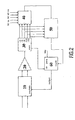
- Fig. 2 shows a block diagram of the prescaler of Fig. 1 .
- the programmable prescaler comprises a 16/17 divider 10, a buffer 20, a divider 30, a decision unit 40, a synchronizing unit 50, and a D-flip-flop 60.
- the 16/17 divider 10 is connected to the buffer 20, which in turn is connected to the divider 30.
- the divider 30 has five output signals, namely /2, /4, /8, /16 and /32 and a zero detection output 'zero'. These five output signals are input to the decision unit 40 and the synchronizing unit 50.
- the decision unit 40 furthermore receives a 5 bit control signal b0, b1, b2, b3 and b4 and the output of the decision unit 40 forms an input to the synchronizing unit 50.
- the output of the synchronizing unit 50 is input to the clock input of the D-flip-flop 60.
- the input 'data' thereof is connected to the supply voltage VDD.
- the output signal 'zero' of divider 30 is connected to the CD input of the D-flip-flop 60.
- the output signal of the D-flip-flop 60 is feedback to the 16/17 divider 10 and input to its 'reclock' input.
- the divider 30 generates the signals /2, /4, /8, /16 and /32, which are input to the decision unit 40. These signals are used to generate a signal which indicates how many pulses should be swallowed, 1, 2, ...., 32. This is performed on the basis of the 5 bit control signal b0, b1, b2, b3 and b4.
- the swallowing of one pulse is performed by delaying one or more pulses, i.e. a frequency division is performed related to your input signal.
- the swallowing of one pulse is identical to a divide-by-2.
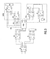
- Fig. 3 shows a block diagram of the 16/17 divider 10 of Fig. 2 .
- the divider 10 comprises a first and second divide-by-2 circuit A, B.
- the second divide-by-2 circuit B is connected with its inputs to the In-phase outputs Ip, In of the first divide-by-2 circuit A.
- a third divide-by-2 circuit C is connected to the quadrature output Qp, Q n of the first divide-by-2 circuit A, and its outputs Ip, In, Qp, Q n are connected to a load Ld.
- the divider 10 comprises a phase selection unit PSU, a retiming unit RTU and a divide-by-four unit UA.
- the retiming unit RTU generates three control signals C0, C1, C2 for controlling the phase switching in the phase selection unit PSU.
- the four phase output signals of the second divide-by-2 circuit B are input to the phase selection unit PSU.
- the phase selection unit PSU selects one of the four phase output signals of the second divide-by-2 circuit B and outputs this signal to the divide-by-four unit UA.
- the third divide-by-2 circuit C is provided for proper loading.
- the retiming unit RTU is provided in order to drive the phase selecting unit PSU and to control the phase switching by the control signals C0, C1, C2.
- the retiming unit RTU comprises a fourth and fifth divide-by-2 circuit D, E and a swallow unit SU.
- the swallow unit determines how many pulses are to be swallowed.
- the divide-by-4 unit UA comprises a sixth and seventh divide-by-2 circuit F, G.
- the input of the sixth divide-by-2 circuit F is connected to the output of the phase selection unit PSU and its In-phase output signals I p , I n are connected to a load Ld, while its quadrature output Q p , Q n is connected to the input of the seventh divide-by-2 circuit.
- the In-phase output signals of the seventh divide-by-2 circuit G constitutes the output of the 16/17 divider 10.
- the phase selecting unit PSU receives the four phase output signals of the second divide-by-2 circuit B as input signals. Since these signals differ by 90° in phase with each other the following signals are provided at the input of the phase selecting unit PSU: INi (0°, Ip), INq (90°, Qp), INni (180°, In) and INnq (270°, Qn).
- the phase selecting unit PSU selects one of the four input signals according to the three control signals C0, C1 and C2 as well as the inversions thereof.
- the output of the phase selecting unit PSU is initially connected to INi, then the output will be connected to INq after an raising edge of INi. Accordingly, the output of the phase selecting unit PSU is delayed with 1/4 T period of the input signals of a phase selecting unit PSU.
- T will be 4*To with To being the period of the input signal of the 16/17 divider 10.
- one complete period To of the input signal is delayed by the phase selection, i.e. a phase switching will result in a delay of one complete period of the input signal of the divider 10.
- the waveforms Ip, Qp, In, Qn correspond to the phases 0°, 90°, 180°, 270° of the second divide-by-2 circuit B, respectively, i.e. the period T thereof equals 4*T0 the period of the input signal of the 16/17 divider.
- the period T thereof equals 4*T0 the period of the input signal of the 16/17 divider.
- the phase selection unit PSU introduces a delay or an extra cycle-slip to its input signal.
- Fig. 4 shows a circuit diagram of a phase selecting unit PSU of Fig. 3 .
- the circuit comprises 22 transistors T1-T22 and four resistors R.
- OUT represents the output signal of the phase selecting unit PSU and INi, INni, INnq, INq represent the four input signals of a phase selecting unit PSU.
- C0, C1 and C2 represent the control signals and NC0, NC1 and NC2 represent the inversions thereof.
- the signal C1 selects between the input signals INi and INni, i.e. between 0° and 180°.
- the signal C2 selects between INq and INnq, i.e. between 90° and 270°.
- the result of the selection according to the control signal C1 is Pi and the result of the selection of the control signal C2 is Pq.
- the control signal C0 selects between the results Pi and Pq.
- the input signal INi is input to the transistor T17, the input signal INni to the transistor T18, the input signal INq to the transistor T20 and the input signal INnq to the transistor T19, respectively.
- the selection is performed according to the states of C1, and C2, in order to achieve the selected signals Pi, Pq.
- the next row of transistors, i.e. T1-T8, is used to select one of the two selection signals Pi, Pq according to the state of the control signal C0.
- the above logic code comprises four branches which are OR-connected.
- the first branch is realized by the transistors T1, T9 and T17.
- the second is implemented by the transistors T1, T11 and T18.
- the third branch is implemented by transistors T3, T13 and T19.
- the fourth branch is implemented by transistors T3, T15 and T20.
- the AND logic function e.g. the first branch NC0•NC1•INi, is implemented differentially by current switching.
- the NAND logic is implemented by differentially switching the inputs in the current domain.
- the OR logic is implemented by adding the output current of the NAND logic in the loads R. The advantage of such an implementation is an increased speed due to the differential implementation in the current domain.
- Fig. 5 shows a block diagram of the phase selecting unit PSU and the retiming unit RTU of Fig. 3 .
- the retiming unit RTU is implemented by a fourth and fifth divide-by-2 circuit D, E.
- the swallow unit SU is implemented by a D-latch DL.
- the D-latch DL receives the output 'out' of the 16/17 divider 10 as data input and a modulator signal 'modul' as clock input.
- the output signals Q, nQ of the D-latch DL are input to the fourth divide-by-2 circuit E, which provides four phase output signals each differing in 90° in phase.
- the In-phase output signal Ip, In thereof constitutes the control signal C0, NC0.
- the quadrature output Qp, Qn thereof is input to the fourth divide-by-2 circuit D.
- the In-phase output signal Ip, In of the fourth divide-by-2 circuit D constitutes the control signal C1, NC1 and the quadrature output signal Q p , Q n constitutes the control signal C2, NC2.
- these three control signals C0, C1 and C2 are input to the phase selecting unit PSU for controlling the phase selection therein.
- the modulator pulse represents the number of phase switching which should occur.
- the signal 'out' represents the previous state of the phase selecting unit PSU, i.e. I, nI, Q, nQ.
- the phase switching is performed in a fixed sequence, namely from I to Q, then to nI and to nQ, i.e. 0°, 90°, 180° and 270°. However, an alternative sequence is also possible.
- Fig. 6 shows a timing diagram of the divider.
- the topmost waveform i.e. VT(div_out) corresponds to the output of the divider.
- the waveform VT(mod_enable) correspond to the modulator input 'modul' of the D-latch DL of the retiming unit RTU.
- the waveform VT(out) corresponds to the output of the phase selection unit PSU.
- the waveform VT(out16) corresponds to the output of the seventh divide-by-2 circuit F, i.e. the output of the 16/17divider 10.
Landscapes
- Stabilization Of Oscillater, Synchronisation, Frequency Synthesizers (AREA)
- Soft Magnetic Materials (AREA)
- Curing Cements, Concrete, And Artificial Stone (AREA)
- Superheterodyne Receivers (AREA)
- Digital Transmission Methods That Use Modulated Carrier Waves (AREA)
Claims (8)
- Prédiviseur à double module à commutation de phase avec un premier et un deuxième modules, comportant un diviseur à double module (10) comportant :- un premier et un deuxième circuits de division par 2 (A ; B), dans lequel ledit deuxième circuit de division par 2 (B) est raccordé à la sortie dudit premier circuit de division par 2 (A) et au moins ledit deuxième circuit de division par 2 (B) comporte quatre sorties de phase (Ip, In, Qp, Qn; INi, INni, INq, INnq), chacune séparée de 90° ;- une unité de sélection de phase (PSU) pour sélectionner l'une des quatre sorties de phase (Ip, In, Qp, Qn ; INi, INni, INq, INnq) du deuxième circuit de division par 2 (B) ;- une unité de contrôle de phase pour (RTU) pour fournir des signaux de contrôle (C1, NC0 ; C2, NC2 ; C3, NC3)1 à l'unité de sélection de phase (PSU),caractérisé en ce que
l'unité de sélection de phase (PSU) est configurée de manière à effectuer la sélection des quatre sorties de phase (Ip, In, Qp, Qn ; INi, INni, INq, INnq) en fonction des signaux de contrôle (C0, NC0 ; C1, NC1 ; C2, NC2) selon une séquence fixe de manière à offrir un décalage de cycle prédéterminé pour la réalisation du deuxième module du prédiviseur ; et
ladite séquence fixe de l'unité de sélection de phase (PSU) étant réalisée grâce à une logique directe, dans laquelle la sortie (OUT) de l'unité de sélection de phase (PSU) est réalisée selon un code logique comprenant des fonctions logiques ET (AND), NON ET (NAND) et OU (OR), dans laquelle lesdites fonctions ET logique sont réalisées de manière différentielle par une commutation de courant, lesdites fonctions NON ET logique sont réalisées par des commutations différentielles des entrées dans le domaine du courant, et dans laquelle lesdites fonctions OU logique sont réalisées par addition du courant de sortie des fonctions NON ET logiques respectives dans des charges correspondantes (R) de telle sorte que la vitesse de ladite unité de sélection de phase (PSU) est augmentée grâce à une réalisation différentielle dans le domaine des courants.
1 La numérotation n'est pas cohérente et n'est pas reprise par la suite. - Prédiviseur selon la revendication 1, dans lequel- la sortie (OUT) de l'unité de sélection de phase (PSU) est réalisée selon le code logique suivant :
 - +, •, ‾ et représentant respectivement les fonctions OU, ET et NON ET.
 - Prédiviseur selon les revendications 1 ou 2, comportant en outre :- un circuit de division par 4 (UA) raccordé à l'entrée de l'unité de sélection de phase (PSU), ledit circuit de division par 4 (UA) comprenant un sixième et un septième circuits de division par 2 (F, G), chacun avec quatre sorties de phase (Ip, In, Qp, Qn) séparées de 90°, ledit septième circuit de division par 2 (G) étant raccordé à la sortie en quadrature (Qp, Qn) du sixième diviseur par 2.
- Prédiviseur selon les revendications 1, 2 ou 3, dans lequel- l'unité de contrôle de phase (RTU) comporte un quatrième et un cinquième circuits de division par 2 (D, E), chacun ayant quatre sorties de phase (Ip, In, Qp, Qn) séparées de 90°, lesdits quatrième et cinquième circuits de division par 2 (D, E) étant raccordés en série,- le signal de sortie en phase (Ip, In) du cinquième circuit de division par 2 (E) correspond au signal de contrôle (C0),- le signal de sortie en phase (Ip, In) du quatrième circuit de division par 2 (D) correspond au signal de contrôle (C1),- le signal de sortie en quadrature (Qp, Qn) du quatrième circuit de division par 2 (E) correspond au signal de contrôle (C2).
- Prédiviseur selon la revendication 4, dans lequel :- l'unité de contrôle de phase (RTU) comprend en outre une bascule D (DL) raccordée à l'entrée du cinquième circuit de division par 2 (E),- la bascule D (DL) reçoit, en tant que signaux d'entrée, l'état précédent de la sortie en phase (Ip, In) du septième circuit de division par 2 (G) et un signal (modul) indiquant le nombre de commutations de phase.
- Prédiviseur selon la revendication 1, dans lequel ledit diviseur à double module (10) est un diviseur 16/17.
- Prédiviseur selon la revendication 1, comprenant en outre une boucle de synchronisation raccordée au diviseur à double module (10) pour la régénération d'horloge du diviseur à double module (10).
- Synthétiseur de fréquence comprenant un prédiviseur selon l'une quelconque des revendications 1 à 7
Priority Applications (1)
| Application Number | Priority Date | Filing Date | Title |
|---|---|---|---|
| EP04770110A EP1671423B1 (fr) | 2003-10-01 | 2004-09-28 | Circuit de division prealable bimodule a commutation de phase |
Applications Claiming Priority (3)
| Application Number | Priority Date | Filing Date | Title |
|---|---|---|---|
| EP03103631 | 2003-10-01 | ||
| EP04770110A EP1671423B1 (fr) | 2003-10-01 | 2004-09-28 | Circuit de division prealable bimodule a commutation de phase |
| PCT/IB2004/051894 WO2005034358A1 (fr) | 2003-10-01 | 2004-09-28 | Circuit de division prealable bimodule a commutation de phase |
Publications (2)
| Publication Number | Publication Date |
|---|---|
| EP1671423A1 EP1671423A1 (fr) | 2006-06-21 |
| EP1671423B1 true EP1671423B1 (fr) | 2008-07-02 |
Family
ID=34400543
Family Applications (1)
| Application Number | Title | Priority Date | Filing Date |
|---|---|---|---|
| EP04770110A Expired - Lifetime EP1671423B1 (fr) | 2003-10-01 | 2004-09-28 | Circuit de division prealable bimodule a commutation de phase |
Country Status (9)
| Country | Link |
|---|---|
| US (1) | US7558361B2 (fr) |
| EP (1) | EP1671423B1 (fr) |
| JP (1) | JP2007508733A (fr) |
| KR (1) | KR101123725B1 (fr) |
| CN (1) | CN1864333B (fr) |
| AT (1) | ATE400087T1 (fr) |
| DE (1) | DE602004014798D1 (fr) |
| TW (1) | TWI342121B (fr) |
| WO (1) | WO2005034358A1 (fr) |
Families Citing this family (7)
| Publication number | Priority date | Publication date | Assignee | Title |
|---|---|---|---|---|
| US7486145B2 (en) * | 2007-01-10 | 2009-02-03 | International Business Machines Corporation | Circuits and methods for implementing sub-integer-N frequency dividers using phase rotators |
| CN100568735C (zh) * | 2007-09-24 | 2009-12-09 | 威盛电子股份有限公司 | 分频器 |
| CN101478307B (zh) * | 2009-01-16 | 2012-05-23 | 复旦大学 | 一种双模4/4.5预分频器 |
| US8451149B2 (en) | 2010-09-27 | 2013-05-28 | St-Ericsson Sa | RF divider using direct digital synthesis |
| TWI469529B (zh) * | 2011-06-03 | 2015-01-11 | Raydium Semiconductor Corp | 非整數頻率時脈產生電路及其方法 |
| US8942299B2 (en) * | 2012-02-27 | 2015-01-27 | Qualcomm Incorporated | Baseband beamforming |
| US10547299B1 (en) * | 2019-01-29 | 2020-01-28 | Texas Instruments Incorporated | Fast transient and low power thin-gate based high-voltage switch |
Family Cites Families (5)
| Publication number | Priority date | Publication date | Assignee | Title |
|---|---|---|---|---|
| KR100207656B1 (ko) * | 1996-02-08 | 1999-07-15 | 윤종용 | 디지털 위상 보정 장치 |
| US6570946B1 (en) * | 1999-11-03 | 2003-05-27 | Ericsson, Inc. | One-hot decoded phase shift prescaler |
| FI108380B (fi) * | 2000-03-10 | 2002-01-15 | Nokia Corp | Monimurtojakajainen esijakaja |
| US6760398B2 (en) * | 2001-10-05 | 2004-07-06 | Asulab S.A. | Switched phase dual-modulus prescaler circuit having means for reducing power consumption |
| AU2002363140A1 (en) * | 2001-10-31 | 2003-05-12 | Sirf Technologies, Inc. | Fractional-r- frequency synthesizer |
-
2004
- 2004-09-28 JP JP2006530938A patent/JP2007508733A/ja active Pending
- 2004-09-28 WO PCT/IB2004/051894 patent/WO2005034358A1/fr not_active Ceased
- 2004-09-28 US US10/573,733 patent/US7558361B2/en not_active Expired - Fee Related
- 2004-09-28 DE DE602004014798T patent/DE602004014798D1/de not_active Expired - Lifetime
- 2004-09-28 EP EP04770110A patent/EP1671423B1/fr not_active Expired - Lifetime
- 2004-09-28 AT AT04770110T patent/ATE400087T1/de not_active IP Right Cessation
- 2004-09-28 KR KR1020067006374A patent/KR101123725B1/ko not_active Expired - Fee Related
- 2004-09-28 CN CN2004800287006A patent/CN1864333B/zh not_active Expired - Fee Related
- 2004-09-30 TW TW093129675A patent/TWI342121B/zh not_active IP Right Cessation
Also Published As
| Publication number | Publication date |
|---|---|
| CN1864333B (zh) | 2012-02-08 |
| EP1671423A1 (fr) | 2006-06-21 |
| JP2007508733A (ja) | 2007-04-05 |
| DE602004014798D1 (de) | 2008-08-14 |
| WO2005034358A1 (fr) | 2005-04-14 |
| TW200516853A (en) | 2005-05-16 |
| KR101123725B1 (ko) | 2012-03-15 |
| ATE400087T1 (de) | 2008-07-15 |
| KR20060090695A (ko) | 2006-08-14 |
| CN1864333A (zh) | 2006-11-15 |
| US20060290433A1 (en) | 2006-12-28 |
| TWI342121B (en) | 2011-05-11 |
| US7558361B2 (en) | 2009-07-07 |
Similar Documents
| Publication | Publication Date | Title |
|---|---|---|
| JP5837617B2 (ja) | オクターブ境界を越えて拡張された同期範囲を有する分周器 | |
| KR101013800B1 (ko) | 멀티-모드 이동 통신 디바이스들을 위한 구성가능한 멀티-모듈러스 주파수 체감기 | |
| KR101575199B1 (ko) | 분주 회로, 주파수 합성기 및 응용 회로 | |
| US6842054B2 (en) | Frequency divider with reduced jitter and apparatus based thereon | |
| EP1575170A1 (fr) | PLL architecture hautement configurable pour un dispositif logique programmable | |
| JP4044819B2 (ja) | 消費電力を低減するための手段を備えた位相切り替えデュアル−モジュラス・プリスケーラ回路 | |
| CN112039521B (zh) | 用于小数分频的四模分频器、小数锁相环及芯片 | |
| US5867068A (en) | Frequency synthesizer using double resolution fractional frequency division | |
| KR20130132305A (ko) | 분수 분주형 주파수 합성기의 광범위 멀티-모듈러스 분할기 | |
| KR100912766B1 (ko) | 주파수 신시사이저를 위한 교환 위상 듀얼-모듈로스프리-스케일러 회로 | |
| JP6484354B2 (ja) | 電子回路、位相ロックループ、送受信機回路、無線局、及び周波数分割の方法 | |
| US8004320B2 (en) | Frequency synthesizer, frequency prescaler thereof, and frequency synthesizing method thereof | |
| US7558361B2 (en) | Phase-switching dual modulus prescaler | |
| US7813466B2 (en) | Jitter-free divider | |
| US5892405A (en) | PLL synthesizer apparatus | |
| JP2017512446A (ja) | 周波数シンセサイザ | |
| EP0780976B1 (fr) | Déphaseur numérique avec diviseur de fréquence | |
| EP1030451A1 (fr) | Boucle à verrouillage de phase | |
| US6094100A (en) | PLL synthesizer apparatus | |
| CN118573187B (zh) | 一种分频电路及数字信号处理电路 | |
| JP2005277665A (ja) | Pllシンセサイザ | |
| CN120128164A (zh) | 高速分频器、多模分频器、锁相环电路、芯片及电子设备 | |
| KR20000000262A (ko) | 새로운 구조의 프로그램어블 주파수 분주기 |
Legal Events
| Date | Code | Title | Description |
|---|---|---|---|
| PUAI | Public reference made under article 153(3) epc to a published international application that has entered the european phase |
Free format text: ORIGINAL CODE: 0009012 |
|
| 17P | Request for examination filed |
Effective date: 20060502 |
|
| AK | Designated contracting states |
Kind code of ref document: A1 Designated state(s): AT BE BG CH CY CZ DE DK EE ES FI FR GB GR HU IE IT LI LU MC NL PL PT RO SE SI SK TR |
|
| DAX | Request for extension of the european patent (deleted) | ||
| 17Q | First examination report despatched |
Effective date: 20070430 |
|
| RAP1 | Party data changed (applicant data changed or rights of an application transferred) |
Owner name: NXP B.V. |
|
| GRAP | Despatch of communication of intention to grant a patent |
Free format text: ORIGINAL CODE: EPIDOSNIGR1 |
|
| GRAS | Grant fee paid |
Free format text: ORIGINAL CODE: EPIDOSNIGR3 |
|
| GRAA | (expected) grant |
Free format text: ORIGINAL CODE: 0009210 |
|
| AK | Designated contracting states |
Kind code of ref document: B1 Designated state(s): AT BE BG CH CY CZ DE DK EE ES FI FR GB GR HU IE IT LI LU MC NL PL PT RO SE SI SK TR |
|
| REG | Reference to a national code |
Ref country code: GB Ref legal event code: FG4D |
|
| REG | Reference to a national code |
Ref country code: CH Ref legal event code: EP |
|
| REF | Corresponds to: |
Ref document number: 602004014798 Country of ref document: DE Date of ref document: 20080814 Kind code of ref document: P |
|
| REG | Reference to a national code |
Ref country code: IE Ref legal event code: FG4D |
|
| PG25 | Lapsed in a contracting state [announced via postgrant information from national office to epo] |
Ref country code: SI Free format text: LAPSE BECAUSE OF FAILURE TO SUBMIT A TRANSLATION OF THE DESCRIPTION OR TO PAY THE FEE WITHIN THE PRESCRIBED TIME-LIMIT Effective date: 20080702 |
|
| PG25 | Lapsed in a contracting state [announced via postgrant information from national office to epo] |
Ref country code: NL Free format text: LAPSE BECAUSE OF FAILURE TO SUBMIT A TRANSLATION OF THE DESCRIPTION OR TO PAY THE FEE WITHIN THE PRESCRIBED TIME-LIMIT Effective date: 20080702 |
|
| NLV1 | Nl: lapsed or annulled due to failure to fulfill the requirements of art. 29p and 29m of the patents act | ||
| PG25 | Lapsed in a contracting state [announced via postgrant information from national office to epo] |
Ref country code: ES Free format text: LAPSE BECAUSE OF FAILURE TO SUBMIT A TRANSLATION OF THE DESCRIPTION OR TO PAY THE FEE WITHIN THE PRESCRIBED TIME-LIMIT Effective date: 20081013 Ref country code: PT Free format text: LAPSE BECAUSE OF FAILURE TO SUBMIT A TRANSLATION OF THE DESCRIPTION OR TO PAY THE FEE WITHIN THE PRESCRIBED TIME-LIMIT Effective date: 20081202 |
|
| PG25 | Lapsed in a contracting state [announced via postgrant information from national office to epo] |
Ref country code: AT Free format text: LAPSE BECAUSE OF FAILURE TO SUBMIT A TRANSLATION OF THE DESCRIPTION OR TO PAY THE FEE WITHIN THE PRESCRIBED TIME-LIMIT Effective date: 20080702 Ref country code: BG Free format text: LAPSE BECAUSE OF FAILURE TO SUBMIT A TRANSLATION OF THE DESCRIPTION OR TO PAY THE FEE WITHIN THE PRESCRIBED TIME-LIMIT Effective date: 20081002 Ref country code: FI Free format text: LAPSE BECAUSE OF FAILURE TO SUBMIT A TRANSLATION OF THE DESCRIPTION OR TO PAY THE FEE WITHIN THE PRESCRIBED TIME-LIMIT Effective date: 20080702 |
|
| PG25 | Lapsed in a contracting state [announced via postgrant information from national office to epo] |
Ref country code: BE Free format text: LAPSE BECAUSE OF FAILURE TO SUBMIT A TRANSLATION OF THE DESCRIPTION OR TO PAY THE FEE WITHIN THE PRESCRIBED TIME-LIMIT Effective date: 20080702 |
|
| PG25 | Lapsed in a contracting state [announced via postgrant information from national office to epo] |
Ref country code: MC Free format text: LAPSE BECAUSE OF NON-PAYMENT OF DUE FEES Effective date: 20080930 Ref country code: DK Free format text: LAPSE BECAUSE OF FAILURE TO SUBMIT A TRANSLATION OF THE DESCRIPTION OR TO PAY THE FEE WITHIN THE PRESCRIBED TIME-LIMIT Effective date: 20080702 Ref country code: EE Free format text: LAPSE BECAUSE OF FAILURE TO SUBMIT A TRANSLATION OF THE DESCRIPTION OR TO PAY THE FEE WITHIN THE PRESCRIBED TIME-LIMIT Effective date: 20080702 |
|
| REG | Reference to a national code |
Ref country code: CH Ref legal event code: PL |
|
| PLBE | No opposition filed within time limit |
Free format text: ORIGINAL CODE: 0009261 |
|
| STAA | Information on the status of an ep patent application or granted ep patent |
Free format text: STATUS: NO OPPOSITION FILED WITHIN TIME LIMIT |
|
| PG25 | Lapsed in a contracting state [announced via postgrant information from national office to epo] |
Ref country code: RO Free format text: LAPSE BECAUSE OF FAILURE TO SUBMIT A TRANSLATION OF THE DESCRIPTION OR TO PAY THE FEE WITHIN THE PRESCRIBED TIME-LIMIT Effective date: 20080702 Ref country code: SK Free format text: LAPSE BECAUSE OF FAILURE TO SUBMIT A TRANSLATION OF THE DESCRIPTION OR TO PAY THE FEE WITHIN THE PRESCRIBED TIME-LIMIT Effective date: 20080702 Ref country code: CZ Free format text: LAPSE BECAUSE OF FAILURE TO SUBMIT A TRANSLATION OF THE DESCRIPTION OR TO PAY THE FEE WITHIN THE PRESCRIBED TIME-LIMIT Effective date: 20080702 |
|
| 26N | No opposition filed |
Effective date: 20090403 |
|
| REG | Reference to a national code |
Ref country code: IE Ref legal event code: MM4A |
|
| PG25 | Lapsed in a contracting state [announced via postgrant information from national office to epo] |
Ref country code: IE Free format text: LAPSE BECAUSE OF NON-PAYMENT OF DUE FEES Effective date: 20080928 |
|
| PG25 | Lapsed in a contracting state [announced via postgrant information from national office to epo] |
Ref country code: IT Free format text: LAPSE BECAUSE OF FAILURE TO SUBMIT A TRANSLATION OF THE DESCRIPTION OR TO PAY THE FEE WITHIN THE PRESCRIBED TIME-LIMIT Effective date: 20080702 |
|
| PG25 | Lapsed in a contracting state [announced via postgrant information from national office to epo] |
Ref country code: CH Free format text: LAPSE BECAUSE OF NON-PAYMENT OF DUE FEES Effective date: 20080930 Ref country code: LI Free format text: LAPSE BECAUSE OF NON-PAYMENT OF DUE FEES Effective date: 20080930 |
|
| PG25 | Lapsed in a contracting state [announced via postgrant information from national office to epo] |
Ref country code: SE Free format text: LAPSE BECAUSE OF FAILURE TO SUBMIT A TRANSLATION OF THE DESCRIPTION OR TO PAY THE FEE WITHIN THE PRESCRIBED TIME-LIMIT Effective date: 20081002 |
|
| PG25 | Lapsed in a contracting state [announced via postgrant information from national office to epo] |
Ref country code: PL Free format text: LAPSE BECAUSE OF FAILURE TO SUBMIT A TRANSLATION OF THE DESCRIPTION OR TO PAY THE FEE WITHIN THE PRESCRIBED TIME-LIMIT Effective date: 20080702 |
|
| PG25 | Lapsed in a contracting state [announced via postgrant information from national office to epo] |
Ref country code: HU Free format text: LAPSE BECAUSE OF FAILURE TO SUBMIT A TRANSLATION OF THE DESCRIPTION OR TO PAY THE FEE WITHIN THE PRESCRIBED TIME-LIMIT Effective date: 20090103 Ref country code: CY Free format text: LAPSE BECAUSE OF FAILURE TO SUBMIT A TRANSLATION OF THE DESCRIPTION OR TO PAY THE FEE WITHIN THE PRESCRIBED TIME-LIMIT Effective date: 20080702 Ref country code: LU Free format text: LAPSE BECAUSE OF NON-PAYMENT OF DUE FEES Effective date: 20080928 |
|
| PG25 | Lapsed in a contracting state [announced via postgrant information from national office to epo] |
Ref country code: TR Free format text: LAPSE BECAUSE OF FAILURE TO SUBMIT A TRANSLATION OF THE DESCRIPTION OR TO PAY THE FEE WITHIN THE PRESCRIBED TIME-LIMIT Effective date: 20080702 |
|
| PG25 | Lapsed in a contracting state [announced via postgrant information from national office to epo] |
Ref country code: GR Free format text: LAPSE BECAUSE OF FAILURE TO SUBMIT A TRANSLATION OF THE DESCRIPTION OR TO PAY THE FEE WITHIN THE PRESCRIBED TIME-LIMIT Effective date: 20081003 |
|
| REG | Reference to a national code |
Ref country code: FR Ref legal event code: PLFP Year of fee payment: 13 |
|
| REG | Reference to a national code |
Ref country code: DE Ref legal event code: R082 Ref document number: 602004014798 Country of ref document: DE Representative=s name: GRUENECKER PATENT- UND RECHTSANWAELTE PARTG MB, DE Ref country code: DE Ref legal event code: R081 Ref document number: 602004014798 Country of ref document: DE Owner name: OCT CIRCUIT TECHNOLOGIES INTERNATIONAL LTD., IE Free format text: FORMER OWNER: NXP B.V., EINDHOVEN, NL |
|
| REG | Reference to a national code |
Ref country code: FR Ref legal event code: PLFP Year of fee payment: 14 |
|
| PGFP | Annual fee paid to national office [announced via postgrant information from national office to epo] |
Ref country code: FR Payment date: 20170822 Year of fee payment: 14 Ref country code: DE Payment date: 20170821 Year of fee payment: 14 Ref country code: GB Payment date: 20170821 Year of fee payment: 14 |
|
| REG | Reference to a national code |
Ref country code: DE Ref legal event code: R119 Ref document number: 602004014798 Country of ref document: DE |
|
| GBPC | Gb: european patent ceased through non-payment of renewal fee |
Effective date: 20180928 |
|
| PG25 | Lapsed in a contracting state [announced via postgrant information from national office to epo] |
Ref country code: DE Free format text: LAPSE BECAUSE OF NON-PAYMENT OF DUE FEES Effective date: 20190402 |
|
| PG25 | Lapsed in a contracting state [announced via postgrant information from national office to epo] |
Ref country code: FR Free format text: LAPSE BECAUSE OF NON-PAYMENT OF DUE FEES Effective date: 20180930 |
|
| PG25 | Lapsed in a contracting state [announced via postgrant information from national office to epo] |
Ref country code: GB Free format text: LAPSE BECAUSE OF NON-PAYMENT OF DUE FEES Effective date: 20180928 |