EP1672397A2 - Verfahren zur Brechungsindexverteilung in einem Lichtübertragungspfad, optischer Filter und Verfahren zu dessen Verwendung - Google Patents
Verfahren zur Brechungsindexverteilung in einem Lichtübertragungspfad, optischer Filter und Verfahren zu dessen Verwendung Download PDFInfo
- Publication number
- EP1672397A2 EP1672397A2 EP06005525A EP06005525A EP1672397A2 EP 1672397 A2 EP1672397 A2 EP 1672397A2 EP 06005525 A EP06005525 A EP 06005525A EP 06005525 A EP06005525 A EP 06005525A EP 1672397 A2 EP1672397 A2 EP 1672397A2
- Authority
- EP
- European Patent Office
- Prior art keywords
- refractive index
- transmission path
- light transmission
- core
- forming
- Prior art date
- Legal status (The legal status is an assumption and is not a legal conclusion. Google has not performed a legal analysis and makes no representation as to the accuracy of the status listed.)
- Withdrawn
Links
- 238000009826 distribution Methods 0.000 title claims abstract description 48
- 230000005540 biological transmission Effects 0.000 title claims abstract description 45
- 238000000034 method Methods 0.000 title claims abstract description 42
- 230000003287 optical effect Effects 0.000 title description 22
- 239000000463 material Substances 0.000 claims abstract description 19
- 230000000737 periodic effect Effects 0.000 claims abstract description 15
- 238000000206 photolithography Methods 0.000 claims abstract description 8
- 239000013307 optical fiber Substances 0.000 claims description 37
- 239000011347 resin Substances 0.000 claims description 14
- 229920005989 resin Polymers 0.000 claims description 14
- 230000001678 irradiating effect Effects 0.000 claims description 8
- VYPSYNLAJGMNEJ-UHFFFAOYSA-N Silicium dioxide Chemical compound O=[Si]=O VYPSYNLAJGMNEJ-UHFFFAOYSA-N 0.000 claims description 6
- 238000000059 patterning Methods 0.000 claims description 5
- 229920003229 poly(methyl methacrylate) Polymers 0.000 claims description 5
- 239000004926 polymethyl methacrylate Substances 0.000 claims description 5
- 230000002829 reductive effect Effects 0.000 claims description 5
- 230000003014 reinforcing effect Effects 0.000 claims description 5
- 239000000377 silicon dioxide Substances 0.000 claims description 3
- 239000010410 layer Substances 0.000 description 58
- 229910052751 metal Inorganic materials 0.000 description 20
- 239000002184 metal Substances 0.000 description 20
- 239000010408 film Substances 0.000 description 15
- 230000008859 change Effects 0.000 description 8
- 230000004044 response Effects 0.000 description 6
- 238000007796 conventional method Methods 0.000 description 5
- KRHYYFGTRYWZRS-UHFFFAOYSA-N Fluorane Chemical compound F KRHYYFGTRYWZRS-UHFFFAOYSA-N 0.000 description 4
- 239000000835 fiber Substances 0.000 description 3
- 230000036961 partial effect Effects 0.000 description 3
- 239000010409 thin film Substances 0.000 description 3
- 229910052721 tungsten Inorganic materials 0.000 description 3
- 230000015572 biosynthetic process Effects 0.000 description 2
- 238000005253 cladding Methods 0.000 description 2
- 230000002452 interceptive effect Effects 0.000 description 2
- 238000004806 packaging method and process Methods 0.000 description 2
- 230000008569 process Effects 0.000 description 2
- 230000005855 radiation Effects 0.000 description 2
- 230000003068 static effect Effects 0.000 description 2
- OKTJSMMVPCPJKN-UHFFFAOYSA-N Carbon Chemical compound [C] OKTJSMMVPCPJKN-UHFFFAOYSA-N 0.000 description 1
- 229910052581 Si3N4 Inorganic materials 0.000 description 1
- 238000001015 X-ray lithography Methods 0.000 description 1
- 229910052799 carbon Inorganic materials 0.000 description 1
- 238000001914 filtration Methods 0.000 description 1
- 230000003993 interaction Effects 0.000 description 1
- 239000013067 intermediate product Substances 0.000 description 1
- 230000000670 limiting effect Effects 0.000 description 1
- 230000010287 polarization Effects 0.000 description 1
- 238000002310 reflectometry Methods 0.000 description 1
- 239000004065 semiconductor Substances 0.000 description 1
- HBMJWWWQQXIZIP-UHFFFAOYSA-N silicon carbide Chemical compound [Si+]#[C-] HBMJWWWQQXIZIP-UHFFFAOYSA-N 0.000 description 1
- 229910010271 silicon carbide Inorganic materials 0.000 description 1
- HQVNEWCFYHHQES-UHFFFAOYSA-N silicon nitride Chemical compound N12[Si]34N5[Si]62N3[Si]51N64 HQVNEWCFYHHQES-UHFFFAOYSA-N 0.000 description 1
- 238000001228 spectrum Methods 0.000 description 1
- 238000004544 sputter deposition Methods 0.000 description 1
- 239000002344 surface layer Substances 0.000 description 1
- 238000002834 transmittance Methods 0.000 description 1
- WFKWXMTUELFFGS-UHFFFAOYSA-N tungsten Chemical compound [W] WFKWXMTUELFFGS-UHFFFAOYSA-N 0.000 description 1
- 239000010937 tungsten Substances 0.000 description 1
- 238000001771 vacuum deposition Methods 0.000 description 1
Images


Classifications
-
- G—PHYSICS
- G02—OPTICS
- G02B—OPTICAL ELEMENTS, SYSTEMS OR APPARATUS
- G02B6/00—Light guides; Structural details of arrangements comprising light guides and other optical elements, e.g. couplings
- G02B6/02—Optical fibres with cladding with or without a coating
- G02B6/02057—Optical fibres with cladding with or without a coating comprising gratings
- G02B6/02076—Refractive index modulation gratings, e.g. Bragg gratings
- G02B6/02123—Refractive index modulation gratings, e.g. Bragg gratings characterised by the method of manufacture of the grating
- G02B6/02142—Refractive index modulation gratings, e.g. Bragg gratings characterised by the method of manufacture of the grating based on illuminating or irradiating an amplitude mask, i.e. a mask having a repetitive intensity modulating pattern
-
- G—PHYSICS
- G02—OPTICS
- G02B—OPTICAL ELEMENTS, SYSTEMS OR APPARATUS
- G02B6/00—Light guides; Structural details of arrangements comprising light guides and other optical elements, e.g. couplings
- G02B6/02—Optical fibres with cladding with or without a coating
- G02B6/02057—Optical fibres with cladding with or without a coating comprising gratings
- G02B6/02076—Refractive index modulation gratings, e.g. Bragg gratings
- G02B6/02123—Refractive index modulation gratings, e.g. Bragg gratings characterised by the method of manufacture of the grating
- G02B6/02133—Refractive index modulation gratings, e.g. Bragg gratings characterised by the method of manufacture of the grating using beam interference
- G02B6/02138—Refractive index modulation gratings, e.g. Bragg gratings characterised by the method of manufacture of the grating using beam interference based on illuminating a phase mask
-
- G—PHYSICS
- G02—OPTICS
- G02B—OPTICAL ELEMENTS, SYSTEMS OR APPARATUS
- G02B6/00—Light guides; Structural details of arrangements comprising light guides and other optical elements, e.g. couplings
- G02B6/02—Optical fibres with cladding with or without a coating
- G02B6/02057—Optical fibres with cladding with or without a coating comprising gratings
- G02B6/02076—Refractive index modulation gratings, e.g. Bragg gratings
- G02B6/02195—Refractive index modulation gratings, e.g. Bragg gratings characterised by means for tuning the grating
- G02B6/022—Refractive index modulation gratings, e.g. Bragg gratings characterised by means for tuning the grating using mechanical stress, e.g. tuning by compression or elongation, special geometrical shapes such as "dog-bone" or taper
Definitions
- a method of forming a periodic refractive index distribution in a light transmission path comprises the steps of: preparing a light transmission path including a core and a clad layer; applying a photosensitive material layer onto the surface of said clad layer; patterning said photosensitive material layer through photolithography thereby forming a mask pattern; and irradiating said light transmission path with an X-ray wave through said mask pattern thereby forming a periodic refractive index fluctuation distribution corresponding to said mask pattern in said core, said permanent refractive index fluctuation distribution remaining unchanged after said irradiation with said X-ray wave.
- an optical mask corresponding to the refractive index fluctuation distribution to be formed in the light transmission path is directly formed on the outer surface of the light transmission path, or a previously formed plane mask is arranged in proximity to the outer surface of an optical fiber member, whereby no complicated optical system is required for forming an interference or diffraction fringe dissimilarly to the prior art and no long time is required for forming a remaining permanent refractive index distribution dissimilarly to the conventional method employing a slit, while the refractive index distribution can be dynamically controlled during irradiation with light by changing the intensity of the light or a region irradiated with the light.
- it is not necessary to utilize interference or diffraction whereby an X-ray having higher efficiency of causing refractive index change than ultraviolet light can be employed to enable formation of a permanent refractive index distribution in a shorter time, while the response speed of response for dynamically controlling the refractive index distribution
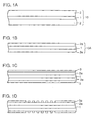
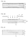
- Figs. 1A to 1D and 2A to 2C are sectional views schematically illustrating a first method of forming a refractive index distribution in a light transmission path.
- the light transmission path includes an optical fiber member or a plane waveguide path which is generally applied to optical communication, while the application thereof is not necessarily restricted to this.
- the light transmission path may include a core part having a high refractive index and a clad part of a surface layer having a lower refractive index than the core part.
- a light transmission path comprising a periodic fringy shielding pattern on its surface as shown in Fig. 2B or Fig. 3C can be employed as an optical filter whose control transmission characteristics can be dynamically controlled.
Landscapes
- Physics & Mathematics (AREA)
- Engineering & Computer Science (AREA)
- Manufacturing & Machinery (AREA)
- General Physics & Mathematics (AREA)
- Optics & Photonics (AREA)
- Optical Integrated Circuits (AREA)
Applications Claiming Priority (3)
| Application Number | Priority Date | Filing Date | Title |
|---|---|---|---|
| JP8236095 | 1995-04-07 | ||
| JP28839695 | 1995-11-07 | ||
| EP96103417A EP0736783B1 (de) | 1995-04-07 | 1996-03-05 | Verfahren zur Herstellung einer Brechungsindexquerschnittverteilung in einem optischen Weg, optischer Filter und Verfahren zur Verwendung dieses Filters |
Related Parent Applications (1)
| Application Number | Title | Priority Date | Filing Date |
|---|---|---|---|
| EP96103417A Division EP0736783B1 (de) | 1995-04-07 | 1996-03-05 | Verfahren zur Herstellung einer Brechungsindexquerschnittverteilung in einem optischen Weg, optischer Filter und Verfahren zur Verwendung dieses Filters |
Publications (2)
| Publication Number | Publication Date |
|---|---|
| EP1672397A2 true EP1672397A2 (de) | 2006-06-21 |
| EP1672397A3 EP1672397A3 (de) | 2006-09-13 |
Family
ID=26423400
Family Applications (2)
| Application Number | Title | Priority Date | Filing Date |
|---|---|---|---|
| EP96103417A Expired - Lifetime EP0736783B1 (de) | 1995-04-07 | 1996-03-05 | Verfahren zur Herstellung einer Brechungsindexquerschnittverteilung in einem optischen Weg, optischer Filter und Verfahren zur Verwendung dieses Filters |
| EP06005525A Withdrawn EP1672397A3 (de) | 1995-04-07 | 1996-03-05 | Verfahren zur Brechungsindexverteilung in einem Lichtübertragungspfad, optischer Filter und Verfahren zu dessen Verwendung |
Family Applications Before (1)
| Application Number | Title | Priority Date | Filing Date |
|---|---|---|---|
| EP96103417A Expired - Lifetime EP0736783B1 (de) | 1995-04-07 | 1996-03-05 | Verfahren zur Herstellung einer Brechungsindexquerschnittverteilung in einem optischen Weg, optischer Filter und Verfahren zur Verwendung dieses Filters |
Country Status (4)
| Country | Link |
|---|---|
| US (1) | US5633966A (de) |
| EP (2) | EP0736783B1 (de) |
| CA (1) | CA2170233C (de) |
| DE (1) | DE69637575D1 (de) |
Cited By (2)
| Publication number | Priority date | Publication date | Assignee | Title |
|---|---|---|---|---|
| CN103137234A (zh) * | 2011-12-02 | 2013-06-05 | 佳能株式会社 | X射线波导和x射线波导系统 |
| CN103137233A (zh) * | 2011-12-02 | 2013-06-05 | 佳能株式会社 | X射线波导和x射线波导系统 |
Families Citing this family (22)
| Publication number | Priority date | Publication date | Assignee | Title |
|---|---|---|---|---|
| WO1996036892A1 (en) * | 1995-05-19 | 1996-11-21 | Cornell Research Foundation, Inc. | Cascaded self-induced holography |
| WO1997001782A1 (en) * | 1995-06-28 | 1997-01-16 | Akzo Nobel N.V. | At least penta-layered optical device |
| JP3929495B2 (ja) * | 1996-01-18 | 2007-06-13 | ブリティッシュ・テレコミュニケーションズ・パブリック・リミテッド・カンパニー | 光感応性屈折率クラッドを備えた光導波路 |
| US6272886B1 (en) | 1996-10-23 | 2001-08-14 | 3M Innovative Properties Company | Incremental method of producing multiple UV-induced gratings on a single optical fiber |
| CA2202308C (en) * | 1996-04-19 | 2001-05-08 | Michihiro Nakai | Optical waveguide grating and production method therefor |
| CA2207226C (en) * | 1996-06-10 | 2005-06-21 | Sumitomo Electric Industries, Ltd. | Optical fiber grating and method of manufacturing the same |
| AU729612B2 (en) * | 1996-11-19 | 2001-02-08 | Alcatel | Optical waveguide with Bragg grating |
| DE19647789A1 (de) * | 1996-11-19 | 1998-05-20 | Alsthom Cge Alcatel | Planarer optischer Wellenleiter, Planarer optischer Wellenleiter mit Bragg-Gitter und Herstellungsverfahren hierfür |
| US5995697A (en) * | 1997-11-19 | 1999-11-30 | Northern Telecom Limited | Partially coated grating optical fibre, method of producing same and fibre telecommunications system |
| US6130973A (en) * | 1998-03-26 | 2000-10-10 | Institut National D'optique | Method and apparatus for spectrally designing all-fiber filters |
| EP0952470A3 (de) * | 1998-04-23 | 2004-01-14 | Nec Corporation | Verfahren zur Herstellung einen optischen Vielfachhalbleiterwellenleiter und einer vielfachstrukturierten optische Halbleitervorrichtung |
| WO2000007049A1 (en) * | 1998-07-24 | 2000-02-10 | Akzo Nobel N.V. | Optical waveguide component |
| GB2340956A (en) * | 1998-08-22 | 2000-03-01 | Marconi Gec Ltd | Controlling the propagation time of an optical delay line using radiation |
| KR100318744B1 (ko) * | 2000-02-21 | 2001-12-28 | 윤종용 | 광파이버를 이용한 액정 디스플레이어의 후방 조명장치 |
| US6596201B1 (en) * | 2000-06-30 | 2003-07-22 | Corning Incorporated | Patterning an optical property on an optical element |
| US6928224B2 (en) | 2001-03-09 | 2005-08-09 | Corning Incorporated | Laser-induced crystallization of transparent glass-ceramics |
| US6904201B1 (en) * | 2001-05-09 | 2005-06-07 | Intel Corporation | Phase-controlled fiber Bragg gratings and manufacturing methods |
| US8805136B2 (en) * | 2006-05-08 | 2014-08-12 | Photonics On-Fiber Devices, Inc. | On-fiber tunable Bragg gratings for DWDM applications |
| WO2013184136A1 (en) * | 2012-06-08 | 2013-12-12 | Empire Technology Development Llc | Multi-frequency filter arrays for low cost spectrometers |
| JP5850992B1 (ja) * | 2014-07-30 | 2016-02-03 | 株式会社フジクラ | 光デバイス、及び、光デバイスの製造方法 |
| US11009657B2 (en) | 2018-09-10 | 2021-05-18 | Nlight, Inc. | Optical fiber splice encapsulated by a cladding light stripper |
| EP3841411B1 (de) * | 2018-09-21 | 2024-11-06 | NLIGHT, Inc. | Lichtabstreifer für den mantel einer optischen faser |
Family Cites Families (9)
| Publication number | Priority date | Publication date | Assignee | Title |
|---|---|---|---|---|
| CA1149209A (en) * | 1980-07-09 | 1983-07-05 | Paolo G. Cielo | Evanescent-wave fiber reflector |
| JPH02188729A (ja) * | 1989-01-17 | 1990-07-24 | Sharp Corp | 光学素子の回析格子製造方法 |
| US5042898A (en) * | 1989-12-26 | 1991-08-27 | United Technologies Corporation | Incorporated Bragg filter temperature compensated optical waveguide device |
| US5048913A (en) * | 1989-12-26 | 1991-09-17 | United Technologies Corporation | Optical waveguide embedded transverse spatial mode discrimination filter |
| FR2657967B1 (fr) * | 1990-02-06 | 1992-05-22 | Bertin & Cie | Procede de realisation d'un reseau d'indice dans une fibre optique, et reseau de capteurs quasi-distribue forme dans cette fibre. |
| US5066133A (en) * | 1990-10-18 | 1991-11-19 | United Technologies Corporation | Extended length embedded Bragg grating manufacturing method and arrangement |
| US5104209A (en) * | 1991-02-19 | 1992-04-14 | Her Majesty The Queen In Right Of Canada, As Represented By The Minister Of Communications | Method of creating an index grating in an optical fiber and a mode converter using the index grating |
| US5388173A (en) * | 1993-12-20 | 1995-02-07 | United Technologies Corporation | Method and apparatus for forming aperiodic gratings in optical fibers |
| US5559907A (en) * | 1994-02-17 | 1996-09-24 | Lucent Technologies Inc. | Method of controlling polarization properties of a photo-induced device in an optical waveguide and method of investigating structure of an optical waveguide |
-
1996
- 1996-02-23 CA CA002170233A patent/CA2170233C/en not_active Expired - Fee Related
- 1996-02-23 US US08/593,033 patent/US5633966A/en not_active Expired - Lifetime
- 1996-03-05 DE DE69637575T patent/DE69637575D1/de not_active Expired - Fee Related
- 1996-03-05 EP EP96103417A patent/EP0736783B1/de not_active Expired - Lifetime
- 1996-03-05 EP EP06005525A patent/EP1672397A3/de not_active Withdrawn
Non-Patent Citations (2)
| Title |
|---|
| HILL K O ET AL: "Photosensitivity in optical fibers" ANNU REV MATER SCI; ANNUAL REVIEW OF MATERIALS SCIENCE; ANNUAL REVIEW OF MATERIAL SCIENCE 1993 PUBL BY ANNUAL REVIEWS INC, PALO ALTO, CA, USA, vol. 23, 1993, pages 125-157, XP008067097 * |
| WILLIAMS G M ET AL: "Permanent photowritten optical gratings in irradiated silicate glasses" OPTICS LETTERS USA, vol. 17, no. 7, 1 April 1992 (1992-04-01), pages 532-534, XP002392167 ISSN: 0146-9592 * |
Cited By (2)
| Publication number | Priority date | Publication date | Assignee | Title |
|---|---|---|---|---|
| CN103137234A (zh) * | 2011-12-02 | 2013-06-05 | 佳能株式会社 | X射线波导和x射线波导系统 |
| CN103137233A (zh) * | 2011-12-02 | 2013-06-05 | 佳能株式会社 | X射线波导和x射线波导系统 |
Also Published As
| Publication number | Publication date |
|---|---|
| DE69637575D1 (de) | 2008-08-14 |
| EP0736783A2 (de) | 1996-10-09 |
| CA2170233A1 (en) | 1996-10-08 |
| EP0736783A3 (de) | 1998-06-10 |
| CA2170233C (en) | 2000-10-03 |
| EP0736783B1 (de) | 2008-07-02 |
| EP1672397A3 (de) | 2006-09-13 |
| US5633966A (en) | 1997-05-27 |
Similar Documents
| Publication | Publication Date | Title |
|---|---|---|
| EP0736783B1 (de) | Verfahren zur Herstellung einer Brechungsindexquerschnittverteilung in einem optischen Weg, optischer Filter und Verfahren zur Verwendung dieses Filters | |
| US5327515A (en) | Method for forming a Bragg grating in an optical medium | |
| EP0604039B1 (de) | Methode zur Herstellung von verteilten Bragg-Reflektoren mit variierendem Gitterabstand in optischen Medien | |
| JP4177893B2 (ja) | 光導波管格子 | |
| EP0924546A1 (de) | Anordnung einer optischen Faser mit variablem Braggfilter | |
| AU739886B2 (en) | Method and apparatus for making continuous chirped fiber bragg gratings | |
| US20030186142A1 (en) | Optical grating fabrication process | |
| JPH09508713A (ja) | 光格子 | |
| US5748814A (en) | Method for spatially controlling the period and amplitude of Bragg filters | |
| JPH1195033A (ja) | 回折格子型帯域透過フィルタ及びその製造方法 | |
| US6574395B1 (en) | Photowritten Bragg grating apodization method | |
| US6170297B1 (en) | Jig for manufacturing long period grating filter and apparatus and method for manufacturing long period grating filter using the same | |
| US5708739A (en) | Method and apparatus for photobleaching patterns in irradiated optical waveguides | |
| WO2003032038A1 (en) | Method and apparatus for recording an optical grating in a photosensitive medium | |
| US5730888A (en) | Bragg gratings in waveguides | |
| KR100315672B1 (ko) | 진폭 마스크를 이용한 절족화된 광섬유 격자의 제작 방법 | |
| US6501883B1 (en) | Method and apparatus for recording an optical grating in a photosensitive medium | |
| JPH09189815A (ja) | 光伝送路中に屈折率分布を形成する方法および光フィルタとその使用方法 | |
| US5985523A (en) | Method for irradiating patterns in optical waveguides containing radiation sensitive constituents | |
| JPH11183718A (ja) | 光導波路型回折格子 | |
| JP2000275442A (ja) | 光バンドパスフィルタ | |
| JP3386350B2 (ja) | 光フィルタの製造方法および光フィルタ製造装置 | |
| CA2259350A1 (en) | Method for volume production of optical grating devices with tuning capability | |
| JP3338337B2 (ja) | 光フィルタの製造方法および光フィルタ製造装置 | |
| KR100267516B1 (ko) | 진폭 마스크를 이용한 제파 필터 제조 방법 및 장치 |
Legal Events
| Date | Code | Title | Description |
|---|---|---|---|
| PUAI | Public reference made under article 153(3) epc to a published international application that has entered the european phase |
Free format text: ORIGINAL CODE: 0009012 |
|
| 17P | Request for examination filed |
Effective date: 20060317 |
|
| AC | Divisional application: reference to earlier application |
Ref document number: 0736783 Country of ref document: EP Kind code of ref document: P |
|
| AK | Designated contracting states |
Kind code of ref document: A2 Designated state(s): DE FR GB IT |
|
| PUAL | Search report despatched |
Free format text: ORIGINAL CODE: 0009013 |
|
| AK | Designated contracting states |
Kind code of ref document: A3 Designated state(s): DE FR GB IT |
|
| STAA | Information on the status of an ep patent application or granted ep patent |
Free format text: STATUS: THE APPLICATION HAS BEEN WITHDRAWN |
|
| 18W | Application withdrawn |
Effective date: 20061030 |