EP1672690B2 - Mikrokühlkörper - Google Patents
Mikrokühlkörper Download PDFInfo
- Publication number
- EP1672690B2 EP1672690B2 EP04030201.0A EP04030201A EP1672690B2 EP 1672690 B2 EP1672690 B2 EP 1672690B2 EP 04030201 A EP04030201 A EP 04030201A EP 1672690 B2 EP1672690 B2 EP 1672690B2
- Authority
- EP
- European Patent Office
- Prior art keywords
- micro
- scale
- cooling element
- scale cooling
- heat sink
- Prior art date
- Legal status (The legal status is an assumption and is not a legal conclusion. Google has not performed a legal analysis and makes no representation as to the accuracy of the status listed.)
- Expired - Lifetime
Links
Images



Classifications
-
- H—ELECTRICITY
- H01—ELECTRIC ELEMENTS
- H01S—DEVICES USING THE PROCESS OF LIGHT AMPLIFICATION BY STIMULATED EMISSION OF RADIATION [LASER] TO AMPLIFY OR GENERATE LIGHT; DEVICES USING STIMULATED EMISSION OF ELECTROMAGNETIC RADIATION IN WAVE RANGES OTHER THAN OPTICAL
- H01S5/00—Semiconductor lasers
- H01S5/02—Structural details or components not essential to laser action
- H01S5/024—Arrangements for thermal management
-
- H—ELECTRICITY
- H01—ELECTRIC ELEMENTS
- H01S—DEVICES USING THE PROCESS OF LIGHT AMPLIFICATION BY STIMULATED EMISSION OF RADIATION [LASER] TO AMPLIFY OR GENERATE LIGHT; DEVICES USING STIMULATED EMISSION OF ELECTROMAGNETIC RADIATION IN WAVE RANGES OTHER THAN OPTICAL
- H01S5/00—Semiconductor lasers
- H01S5/40—Arrangement of two or more semiconductor lasers, not provided for in groups H01S5/02 - H01S5/30
- H01S5/4025—Array arrangements, e.g. constituted by discrete laser diodes or laser bar
-
- H—ELECTRICITY
- H10—SEMICONDUCTOR DEVICES; ELECTRIC SOLID-STATE DEVICES NOT OTHERWISE PROVIDED FOR
- H10W—GENERIC PACKAGES, INTERCONNECTIONS, CONNECTORS OR OTHER CONSTRUCTIONAL DETAILS OF DEVICES COVERED BY CLASS H10
- H10W40/00—Arrangements for thermal protection or thermal control
- H10W40/40—Arrangements for thermal protection or thermal control involving heat exchange by flowing fluids
- H10W40/47—Arrangements for thermal protection or thermal control involving heat exchange by flowing fluids by flowing liquids, e.g. forced water cooling
-
- H—ELECTRICITY
- H01—ELECTRIC ELEMENTS
- H01S—DEVICES USING THE PROCESS OF LIGHT AMPLIFICATION BY STIMULATED EMISSION OF RADIATION [LASER] TO AMPLIFY OR GENERATE LIGHT; DEVICES USING STIMULATED EMISSION OF ELECTROMAGNETIC RADIATION IN WAVE RANGES OTHER THAN OPTICAL
- H01S5/00—Semiconductor lasers
- H01S5/02—Structural details or components not essential to laser action
- H01S5/024—Arrangements for thermal management
- H01S5/02407—Active cooling, e.g. the laser temperature is controlled by a thermo-electric cooler or water cooling
- H01S5/02423—Liquid cooling, e.g. a liquid cools a mount of the laser
Definitions
- the present invention relates to a micro heat sink with a mounting surface for a component to be cooled, in particular a semiconductor component, which is in particular cuboid-shaped and has a micro cooling structure inside which is connected via connecting channels to at least one inlet opening and at least one outlet opening, and with these forms a cooling circuit formed within the micro heat sink, via which a cooling medium can be supplied to or removed from the microstructure.
- the invention further relates to a diode laser component with a soldered diode laser or a diode laser stack, which have such micro heat sinks, and a method for producing a micro heat sink.
- Micro heat sinks of the above mentioned type are from the US 5 548 606 A known.
- Micro heat sinks of the above mentioned type are known and for example in the DE 4 315 580 A1
- the micro heat sinks consist of a large number of individual Layers of structured copper foils approximately 300 ⁇ m thick.
- the copper foils are layered on top of each other in a suitable manner such that the structures etched or punched into the copper foils, for example, form a cooling circuit with a micro cooling structure, connecting channels and an inlet and outlet.
- the copper foils are then bonded together using direct copper bonding.
- Oxide layers are formed on the surfaces of the copper layers, which are then welded together.
- a cooling medium such as deionized water flows through the layered micro heat sink.
- deionized water as a cooling medium is considered advantageous because it shows only a low level of interaction with the material of the micro heat sink.
- the problem with direct copper bonding is that the connections formed between the oxide layers have a low tightness, so that the micro heat sink must have a minimum wall thickness of 400 ⁇ m to ensure a minimum level of safety against leakage of the micro heat sink.
- the micro heat sink is susceptible to corrosion.
- the state of the art proposes applying passivation layers, for example made of nickel, to the copper layers.
- passivation layers for example made of nickel
- the flow of deionized water in the micro heat sink removes the passivation layer, particularly at sharp edge areas, and it is absorbed by the deionized water.
- the ions introduced into the deionized water in this way can act as a type of "degradation catalyst". The result is that the copper released in the removed areas may even become more susceptible to corrosion.
- copper has a thermal expansion coefficient of approximately 17, whereas a component to be soldered onto the micro heat sink, such as a high-power diode laser made of gallium arsenide, has a thermal expansion coefficient of approximately 6.5. Due to the different thermal expansion coefficients, stresses and distortion can occur between the micro heat sink and the component being soldered onto it.
- the document DE 195 06 091 A1 proposes to provide ceramic layers between the individual copper layers and to weld the copper layers and the Ceramic layers are bonded together using the direct copper bonding technique.
- the ceramic layers are provided with a copper layer on their outer sides, with a component to be cooled, in this case a diode laser, arranged on the top layer.
- a component to be cooled in this case a diode laser
- the use of the ceramic layers is intended to ensure that the substrate has a greatly reduced coefficient of thermal expansion compared to a substrate or heat sink which consists exclusively of metal and in particular of copper.
- micro heat sink as described in claim 1, which has a monolithic structure.
- the invention is based on the basic idea that the sealing problem is reduced by avoiding joints such as those present in layered micro heat sinks.
- This is achieved by producing a monolithic micro heat sink.
- the monolithic structure of the micro heat sink makes it possible to greatly reduce the required minimum outer wall thickness of the micro heat sink compared to the wall thicknesses of the known copper heat sinks, so that a much larger overlap is achieved between the area through which a cooling medium, for example deionized water, can flow for heat exchange and the area in which the electronic components are soldered on.
- a cooling medium for example deionized water
- the micro heat sink according to the invention is expediently produced by means of selective laser melting.
- the selective laser melting process makes it possible to produce any monolithic, three-dimensional shapes and structures within the micro heat sink.
- outer wall thicknesses of ⁇ 400 ⁇ m can be realized, in particular outer wall thicknesses of approximately 100 ⁇ m, so that the temperature gradient within the soldered electronic components themselves is also reduced.
- the present invention provides for the micro heat sink to be made of stainless steel or molybdenum. Due to the corrosion resistance of stainless steel, the risk of corrosion and, consequently, of leakage of the micro heat sink caused by corrosion is reduced, so that the minimum outer wall thickness can be kept correspondingly low. The resulting improved heat exchange in the overlap area between the micro heat sink and the electrical component compensates for the poorer thermal conductivity of stainless steel compared to copper.
- the micro heat sink be made of a material that is adapted to the thermal expansion coefficient of the component to be cooled.
- a component to be cooled made of gallium arsenide with a thermal expansion coefficient of approximately 6.5 molybdenum with a thermal expansion coefficient of approximately 5 will be selected as the material for the micro heat sink.
- the micro cooling structure can be designed in such a way that a turbulent flow is formed therein, thereby achieving improved cooling performance.
- the micro cooling structure can have comb-shaped extensions arranged at a short distance from one another. Due to the short distances between the comb-shaped extensions, the interfaces that are located close to one another can also influence one another, which in turn leads to an improved cooling effect.
- the connecting channels have a flow-optimized structure, in particular in the form of rounded, in particular oval, inner walls and interfaces, so that an almost laminar flow is formed in the connecting channels.
- a laminar flow is desirable in the area of the connecting channels in order to keep the pressure drop in the cooling medium as low as possible while it flows through the micro heat sink.
- the micro-cooling bodies according to the invention can also be used in so-called diode laser stacks for cooling the diode lasers located therein.
- it is advantageous to design the micro-cooling bodies in a cuboid shape since the micro-cooling bodies according to the invention are stacked on top of one another in the stacks.
- the cuboid-shaped micro-coolers each form a flat support surface for the micro-cooler to be stacked above them, so that a stable connection can be established between the individual micro-coolers.
- the inlet and outlet openings of the individual micro-cooling bodies are connected to a common inlet channel formed in the stack and a common outlet channel for the cooling medium.
- FIGS. 1 and 2 show an embodiment of a micro heat sink 1 according to the invention.
- the micro heat sink 1 is essentially cuboid-shaped and has a mounting surface 2 for a component to be cooled, such as a semiconductor component, on the top side in the front end area.
- a micro cooling structure 3 is arranged below the mounting surface 2 in the interior of the micro heat sink 1, which together with connecting channels 4, at least one inlet opening 5 and at least one outlet opening 6 forms a Cooling circuit 7 is formed, through which a cooling medium, such as deionized water, can flow for cooling purposes.
- the micro-cooling structure 3 is formed in a manner known per se from comb-shaped extensions 8 which are arranged at a small distance from one another so that the interfaces of the comb-shaped extensions 8 can influence one another.
- the connecting channels 4 have a flow-optimized structure in the form of rounded, in particular oval walls and interfaces 4a, so that an almost laminar flow is formed in the connecting channels 4. This reduces a pressure drop in the cooling medium flowing through the micro-cooling body 1.
- the cross-section of the connecting channels 4 decreases towards the micro-cooling structure 3, whereby a turbulent flow is formed in this area. This results in improved heat exchange.
- the formation of a turbulent flow can be further supported by a suitable structuring of the surfaces of the connecting channels 4.
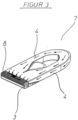
- An example of the flow pattern of the cooling medium in the micro-cooler 1 is shown in the Figure 3 indicated by black arrows.
- the micro heat sink 1 shown in the figures is intended to be used to cool a diode laser bar made of gallium arsenide with a thermal expansion coefficient of approximately 6.5.
- the micro heat sink 1 is therefore made of molybdenum with a thermal expansion coefficient of approximately 5 By adjusting the thermal expansion coefficients of the diode laser bar and the material of the micro heat sink 1, residual stresses can be reduced.
- the micro heat sink 1 is manufactured by means of selective laser melting.
- the component to be manufactured is first virtually cut into sections along the Z plane of the component, and the resulting CAD data in the X and Y directions are entered into a control unit.
- a metallic material powder made of stainless steel or molybdenum, free of binding agents and fluxes, is then applied to a base plate of a process chamber that can be lowered in the Z direction, with a predetermined layer height that corresponds to the penetration depth of a laser beam used in the process.
- a laser beam is moved across the powder layer in accordance with the CAD data entered into the control unit, so that the metallic material powder is locally heated to melting temperature and completely melted over its entire layer height at the respective point of impact of the laser beam.
- the base plate is then lowered by an amount that corresponds to the layer thickness of the filled metal powder.
- another layer of the metallic material powder is applied to the existing metal powder layer treated with laser radiation, the layer thickness of which corresponds to the penetration depth of the laser beam.
- the laser beam is then directed again in the X and Y directions according to the CAD data entered in the control system for the micro heat sink to be produced. and the material at the point of impact of the laser is completely melted over its entire layer thickness. This procedure is repeated until the micro heat sink is completely structured and constructed.
- the laser beam is guided in several tracks over the specified area of the material layer so that each subsequent track of the laser beam partially overlaps the previous track. Due to the overlap, the melt of the powder and the melt of the adjacent, already solidified contour, which was previously melted and lies under the subsequently applied powder layer, are melted into a common melt pool. The melt pool then forms a melt-metallurgical bond. This results in a homogeneous molded body with high strength and tightness and without grooves or other transition points after solidification.
- micro heat sink Once the micro heat sink has been completely constructed in this way, it is then only necessary to remove the powder remaining in the internal structures. This can be achieved, for example, using compressed air or by subsequently flushing the micro heat sink with deionized water under pressure.
Landscapes
- Physics & Mathematics (AREA)
- Condensed Matter Physics & Semiconductors (AREA)
- General Physics & Mathematics (AREA)
- Electromagnetism (AREA)
- Optics & Photonics (AREA)
- Cooling Or The Like Of Semiconductors Or Solid State Devices (AREA)
- Semiconductor Lasers (AREA)
Description
- Die vorliegende Erfindung betrifft einen Mikrokühlkörper mit einer Montagefläche für ein zu kühlendes Bauteil, insbesondere ein Halbleiterbauelement, welcher insbesondere quaderartig ausgebildet ist und im Inneren eine Mikrokühlstruktur aufweist, die über Verbindungskanäle mit mindestens einer Zulauföffnung und mindestens einer Ablauföffnung verbunden ist, und mit diesen einen innerhalb des Mikrokühlkörpers ausgebildeten Kühlkreislauf bilden, über den der Mikrostruktur ein Kühlmedium zuführ- bzw. aus ihr abführbar ist. Weiterhin betrifft die Erfindung ein Diodenlaserbauelement mit einem aufgelöteten Diodenlaser bzw. einen Diodenlaserstack, die solche Mikrokühlkörper aufweisen, sowie ein Verfahren zur Herstellung eines Mikrokühlkörpers.
- Mikrokühlkörper der oben genannten Art sind aus der
US 5 548 606 A bekannt. - Mikrokühlkörper der oben genannten Art sind bekannt und beispielsweise in der
DE 4 315 580 A1 beschrieben. Die Mikrokühlkörper bestehen aus einer Vielzahl von einzelnen Lagen bzw. Schichten strukturierter, etwa 300 µm starker Kupferfolien. - Zur Herstellung des Mikrokühlkörpers werden die Kupferfolien in geeigneter Weise derart übereinander geschichtet, daß die in die Kupferfolien beispielsweise geätzten oder gestanzten Strukturen einen Kühlkreislauf mit einer Mikrokühlstruktur, Verbindungskanälen und einem Zu- und Ablauf bilden.
- Anschließend werden die Kupferfolien durch Direct Copper Bonding miteinander verbunden. Dazu werden an den Oberflächen der Kupferschichten Oxidschichten ausgebildet, die anschließend miteinander verschweißt werden.
- Im Betrieb wird der schichtförmig aufgebaute Mikrokühlkörper mit einem Kühlmedium wie beispielsweise deionisiertem Wasser durchströmt. Der Einsatz von deionisiertem Wasser als Kühlmedium wird als vorteilhaft angesehen, da es nur eine geringe Wechselwirkung mit dem Material des Mikrokühlkörpers zeigt.
- Beim Direct Copper Bonding wird als problematisch angesehen, daß die zwischen den Oxidschichten gebildeten Verbindungen eine geringe Dichtigkeit aufweisen, so daß der Mikrokühlkörper eine Mindestwandstärke von 400 µm aufweisen muß, um ein Mindestmaß an Sicherheit vor einer Leckage des Mikrokühlkörpers zu gewährleisten.
- Weiterhin ist aufgrund der Oxidschichten und dadurch, daß die den kühlkreislauf bildenden Strukturen in die Kupferfolien größtenteils geätzt werden, der Mikrokühlkörper korrosionsanfällig.
- Zur Vermeidung dieser Korrosion wird im Stand der Technik vorgeschlagen, Passivierungsschichten beispielsweise aus Nickel auf die Kupferschichten aufzubringen. Jedoch wird durch die Strömung des deionisierten Wassers in dem Mikrokühlkörper die Passivierungsschicht insbesondere an scharfen Kantenbereichen abgetragen und von dem deionisierten Wasser aufgenommen. Die so in das deionisierte Wasser eingebrachten Ionen können dabei als eine Art "Abbaukatalysator" wirken. Die Folge ist eine ggf. sogar beschleunigte Korrosionsanfälligkeit des an den abgetragenen Bereichen freiwerdenden Kupfers.
- Ein weiteres Problem bei der Verwendung von Mikrokühlkörpern aus Kupfer besteht darin, daß Kupfer einen Wärmeausdehnungskoeffizienten von ungefähr 17 besitzt, wohingegen ein auf den Mikrokühlkörper aufzulötendes Bauteil wie beispielsweise ein Hochleistungsdiodenlaser aus Galliumarsenit einen Wärmeausdehnungskoeffizienten von ungefähr 6,5 aufweist. Aufgrund der unterschiedlichen Wärmeausdehnungskoeffizienten können Spannungen und Verzug zwischen dem Mikrokühlkörper und dem jeweils aufgelöteten Bauteil auftreten.
- Zur Lösung dieses Problems schlägt das Dokument
DE 195 06 091 A1 vor, zwischen den einzelnen Kupferschichten Keramikschichten vorzusehen und die Kupferschichten und die Keramikschichten jeweils unter Verwendung der Direct-Copper-Bonding-Technik flächig miteinander zu verbinden. Die Keramikschichten werden dazu an ihren außen liegenden Seiten mit einer Kupferschicht versehen, wobei auf der obersten Schicht ein zu kühlendes Bauteil, hier einen Diodenlaser, angeordnet ist. Unterhalb der Diodenlaseranordnung ist in der Keramikschicht zur Verbesserung der Wärmeleitfähigkeit ein Einsatz oder eine vergrabene Schicht aus einem Material mit extrem hoher Wärmeleitfähigkeit, beispielsweise Diamant oder T-cBN, eingebracht. Durch die Verwendung der Keramikschichten soll gewährleistet werden, daß das Substrat gegenüber einem Substrat oder Kühlkörper, welcher ausschließlich aus Metall und insbesondere aus Kupfer besteht, einen stark reduzierten Wärmeausdehnungskoeffizienten aufweist. - Bei der aus dem Dokument
DE 195 06 091 A1 bekannten Anordnung geht aufgrund der verwendeten Oxidschichten wie oben bereits erläutert sowohl ein Dichtigkeitsproblem als auch ein Korrosionsproblem einher. Ferner können auch zwischen den Kupfer- und Keramikschichten Eigenspannungen auftreten, die ebenfalls zu einer Leckage führen können. - Es ist daher Aufgabe der vorliegenden Erfindung, einen Mikrokühlkörper sowie ein Verfahren zu dessen Herstellung bereitzustellen, die eine Verringerung der Mindestaußenwandstärken des Mikrokühlkörpers ermöglichen, um eine verbesserte Wärmeabfuhr im Bereich der Montageflächen für elektronische Bauteile zu erreichen, ohne dabei eine Verringerung der Leckagesicherheit des Mikrokühlkörpers in Kauf nehmen zu müssen.
- Diese Aufgabe wird erfindungsgemäß durch einen Mikrokühlkörper wie im Anspruch 1 beschrieben gelöst, welcher eine monolithische Struktur aufweist.
- Mit anderen Worten basiert die Erfindung auf dem Grundgedanken, daß durch die Vermeidung von Fugen, wie sie in schichtförmig aufgebauten Mikrokühlkörpern vorhanden sind, das Dichtigkeitsproblem verringert wird. Dies wird erreicht, indem ein monolithischer Mikrokühlkörper hergestellt wird. Durch die monolithische Struktur des Mikrokühlkörpers ist es möglich, die benötigte Mindestaußenwandstärke des Mikrokühlkörpers gegenüber den Wandstärken der bekannten Kupferwärmesenken stark zu verringern, so daß eine wesentlich größere Überdeckung zwischen dem Bereich, durch den ein Kühlmedium, beispielsweise deionisiertes Wasser, für einen Wärmeaustausch fließen kann und dem Bereich, in dem die elektronischen Bauelemente aufgelötet sind, erreicht wird.
- Zweckmäßigerweise wird der erfindungsgemäße Mikrokühlkörper mittels des selektiven Laserschmelzens hergestellt. Durch das Verfahren des selektiven Laserschmelzens wird es möglich, beliebige monolithische, dreidimensionale Formen und Strukturen innerhalb des Mikrokühlkörpers zu erzeugen.
- In dem erfindungsgemäßen Mikrokühlkörper können Außenwandstärken < 400 µm realisiert werden, insbesondere Außenwandstärken von ungefähr 100 µm, so daß auch der Temperaturgradient innerhalb der aufgelöteten elektronischen Bauelemente selbst verringert wird.
- Die vorliegende Erfindung sieht vor, den Mikrokühlkörper aus Edelstahl oder Molybdän auszubilden. Aufgrund der Korrosionsbeständigkeit des Edelstahls wird die Gefahr von Korrosion und folglich einer durch die Korrosion hervorgerufenen Leckage des Mikrokühlkörpers vermindert, so daß die Mindestaußenwandstärke entsprechend gering gehalten werden kann. Durch den hieraus folgenden verbesserten Wärmeaustausch im Überdeckungsbereich zwischen Mikrokühlkörper und elektrischem Bauelement wird die gegenüber Kupfer an sich schlechtere Wärmeleitfähigkeit des Edelstahls ausgeglichen.
- Um eventuell entstehende Eigenspannungen zwischen den elektronischen Bauteilen und dem Mikrokühlkörper aufgrund der unterschiedlichen Wärmeausdehnungskoeffizienten zu verringern, schlägt die Erfindung vor, den Mikrokühlkörper aus einem an den Wärmeausdehnungskoeffizienten des zu kühlenden Bauteils angepaßten Material auszubilden. Im Falle eines zu kühlenden Bauteiles aus Galliumarsenit mit einem Wärmeausdehnungkoeffizienten von ungefähr 6,5 wird Molybdän mit einem Wärmeausdehnungskoeffizienten von ungefähr 5 als Material für den Mikrokühlkörper gewählt werden.
- Um den Kühleffekt im Überdeckungsbereich des elektronischen Bauteils mit dem Mikrokühlkörper weiter zu steigern, kann die Mikrokühlstruktur derart ausgeführt sein, daß sich darin eine turbulente Strömung ausbildet, wodurch eine verbesserte Kühlleistung erreicht wird.
- Die Mikrokühlstruktur kann in geringem Abstand zueinander angeordnete kammförmige Fortsätze aufweisen. Durch die geringen Abstände der kammförmigen Fortsätze zueinander können sich die dadurch nahe beieinanderliegenden Grenzflächen auch untereinander beeinflussen, was wiederum zu einer verbesserten Kühlwirkung führt.
- Gemäß einem weiteren Ausführungsbeispiel der Erfindung weisen die Verbindungskanäle eine strömungsoptimierte Struktur, insbesondere in Form von abgerundeten insbesondere ovalen Innenwandungen und Grenzflächen auf, so daß sich in den Verbindungskanälen eine nahezu laminare Strömung ausbildet. Eine laminare Strömung ist im Bereich der Verbindungskanäle wünschenswert, um Druckabfall im Kühlmedium während des Durchströmens des Mikrokühlkörpers möglichst gering zu halten.
- Die erfindungsgemäßen Mikrokühlkörper können auch in sogenannten Diodenlaserstacks zur Kühlung der darin befindlichen Diodenlaser eingesetzt werden. Für diese Anwendung ist es vorteilhaft, den Mikrokühlkörper quaderförmig auszuführen, da die erfindungsgemäßen Mikrokühlkörper in den Stacks übereinander gestapelt werden. Die quaderförmigen Mikrokühler bilden jeweils eine ebene Auflägefläche für den darüber zu stapelnden Mikrokühler, sodaß sich eine stabile Verbindung zwischen den einzelnen Mikrokühlern herstellen läßt. Die Zulauf- bzw. Ablauföffnungen der einzelnen Mikrokühlkörper werden zum Betrieb des Stacks an einen in dem Stack ausgebildeten gemeinsamen Zulaufkanal sowie einen gemeinsamen Ablaufkanal für das Kühlmedium angeschlossen.
- Hinsichtlich weiterer vorteilhafter Ausgestaltungen und Weiterbildungen der Erfindung wird auf die Unteransprüche sowie die nachfolgende Beschreibung eines Ausführungsbeispiels anhand der beiliegenden Zeichnung verwiesen. In der Zeichnung zeigt:
- Figur 1
- eine perspektivische Darstellung eines erfindungsgemäßen Mikrokühlkörpers;
- Figur 2
- einen Längsschnitt durch einen Mikrokühlkörper gemäß der
Figur 1 um 180° gedreht; - Figur 3
- eine perspektivische Darstellung einer in dem Mikrokühlkörper gemäß der
Figur 1 ausgebildeten Kühlkreislauf von oben; und - Figur 4
- eine perspektivische Darstellung des Kühlkreislaufs aus der
Figur 3 von unten. - Die
Figuren 1 und2 zeigen ein Ausführungsbeispiel eines erfindungsgemäßen Mikrokühlkörpers 1. - Der Mikrokühlkörper 1 ist im wesentlichen quaderförmig ausgebildet und weist an der Oberseite im vorderen stirnseitigen Endbereich eine Montagefläche 2 für ein zu kühlendes Bauteil wie beispielsweise ein Halbleiterbauelement auf. Unterhalb der Montagefläche 2 ist im Inneren des Mikrokühlkörpers 1 eine Mikrokühlstruktur 3 angeordnet, die zusammen mit Verbindungskanälen 4, mindestens einer Zulauföffnung 5 und mindestens einer Ablauföffnung 6 einen Kühlkreislauf 7 bildet, welcher zu Kühlzwecken mit einem Kühlmedium, wie beispielsweise mit deionisiertem Wasser, durchströmt werden kann.
- Die Mikrokühlstruktur 3 ist in an sich bekannter Weise aus kammförmigen Fortsätzen 8 ausgebildet, die in geringem Abstand zueinander angeordnet sind, so daß sich die Grenzflächen der kammförmigen Fortsätze 8 untereinander beeinflussen können.
- Wie in den
Figuren 3 und4 zu sehen ist, weisen die Verbindungskanäle 4 eine strömungsoptimierte Struktur in Form von abgerundeten, insbesondere ovalen Wandungen und Grenzflächen 4a auf, so daß sich in den Verbindungskanälen 4 eine nahezu laminare Strömung ausbildet. Dadurch wird ein Druckabfall in dem den Mikrokühlkörper 1 durchströmenden Kühlmedium vermindert. Zur Mikrokühlstruktur 3 hin verringert sich der Querschnitt der Verbindungskanäle 4, wodurch sich in diesem Bereich eine turbulente Strömung ausbildet. Dies hat einen verbesserten Wärmetausch zur Folge. Durch eine geeignete Strukturierung der Oberflächen der Verbindungskanäle 4 kann die Ausbildung einer turbulenten Strömung noch unterstützt werden. Ein beispielhafter Strömungsverlauf des Kühlmediums in dem Mikrokühler 1 ist in derFigur 3 durch schwarze Pfeile angedeutet. - Der in den Figuren gezeigte Mikrokühlkörper 1 soll dazu eingesetzt werden, einen Diodenlaserbarren aus Galliumarsenit mit einem Wärmeausdehnungskoeffizienten von ungefähr 6,5 zu kühlen. Der Mikrokühlkörper 1 ist daher aus Molybdän mit einem Wärmeausdehnungskoeffizienten von ungefähr 5 aufgebaut. Durch die Anpassung der Wärmeausdehnungskoeffizienten des Diodenlaserbarrens und des Materials des Mikrokühlkörpers 1 können Eigenspannungen verringert werden.
- Der Mikrokühlkörper 1 wird mittels des selektiven Laserschmelzens hergestellt. Bei diesem Verfahren wird das herzustellende Bauteil zunächst entlang der Z-Ebene des Bauteils virtuell in Schnitte zerlegt, und die sich daraus ergebenden CAD-Daten in X- und Y-Richtung werden in eine Steuereinheit eingegeben. Anschließend wird ein metallisches Werkstoffpulver aus Edelstahl oder Molybdän frei von Bindemitteln und Flußmitteln mit einer vorgegebenen Schichthöhe, die einer Eindringtiefe eines in dem Verfahren eingesetzten Laserstrahls entspricht auf eine in Z-Richtung versenkbare Bodenplatte einer Prozeßkammer aufgebracht. Unter Schutzgasatmosphäre wird ein Laserstrahl entsprechend der in die Steuereinheit eingegebenen CAD-Daten auf der Pulverschicht verfahren, so daß das metallische Werkstoffpulver lokal auf Schmelztemperatur erhitzt und an der jeweiligen Auftreffstelle des Laserstrahls über seine gesamte Schichthöhe vollständig aufgeschmolzen wird. Anschließend wird die Bodenplatte um einen Betrag abgesenkt, der der Schichtdicke des eingefüllten Metallpulvers entspricht. Dann wird eine weitere Schicht aus dem metallischen Werkstoffpulver auf die bereits vorhandene, mit Laserstrahlung behandelte Metallpulverschicht aufgebracht, deren Schichtdicke wiederum der Eindringtiefe des Laserstrahls entspricht. Danach wird der Laserstrahl erneut entsprechend der in der Steuerung eingegebenen CAD-Daten des herzustellenden Mikrokühlkörpers in X- und Y-Richtung verfahren und das Material an der Auftreffstelle des Lasers wiederum über seine gesamte Schichtdicke vollständig aufgeschmolzen. Diese Vorgehensweise wird solange wiederholt, bis der Mikrokühlkörper vollständig strukturiert und aufgebaut ist.
- Der Laserstrahl wird in mehreren Spuren über den vorgegebenen Bereich der Werstoffschicht so geführt, daß jede folgende Spur des Laserstrahl die vorherige Spur teilweise überlappt. Durch die Überlappung wird die Schmelze des Pulvers und die Schmelze der angrenzenden bereits erstarrten festen Kontur, die zuvor aufgeschmolzen wurde und unter der nachträglich aufgetragenen Pulverschicht liegt, zu einem gemeinsamen Schmelzbad aufgeschmolzen. Daraufhin geht das Schmelzbad eine schmelzmetallurgische Verbindung ein. Dadurch bildet sich nach der Erstarrung ein homogener Formkörper mit hoher Festigkeit und Dichtigkeit und ohne Rillen oder sonstige Übergangsstellen aus.
- Wurde auf diese Weise der Mikrokühlkörper vollständig aufgebaut, so ist es anschließend lediglich notwendig, das in den inneren Strukturen zurückgebliebene Pulver zu entfernen. Dies kann beispielsweise mittels Druckluft erreicht werden oder indem der Mikrokühlkörper anschließend mit deionisiertem Wasser unter Druck durchspült wird.
Claims (9)
- Mikrokühlkörper (1) mit einer Montagefläche (2) für ein zu kühlendes Bauteil, insbesondere ein Halbleiterbauelement, welcher im Inneren eine Mikrokühlstruktur (3) aufweist, die über Verbindungskanäle (4) mit mindestens einer Zulauföffnung (5) und mindestens einer Ablauföffnung (6) verbunden ist, und mit diesen einen innerhalb des Mikrokühlkörpers (1) ausgebildeten Kühlkreislauf (7) bilden, über den der Mikrokühlstruktur (3) ein Kühlmedium zuführ- bzw. aus ihr abführbar ist, dadurch gekennzeichnet, daß der Mikrokühlkörper (1) eine monolithische Struktur aufweist und durch selektives Laserschmelzen hergestellt ist, und wobei der Mikrokühlkörper (1) aus Edelstahl oder Molybdän gebildet ist.
- Mikrokühlkörper (1) nach Anspruch 1, dadurch gekennzeichnet, daß er quaderartig ausgebildet ist.
- Mikrokühlkörper (1) nach Anspruch 1 oder 2, dadurch gekennzeichnet, daß er Außenwandstärken < 400 µm aufweist.
- Mikrokühlkörper (1) nach einem der vorherigen Ansprüche, dadurch gekennzeichnet, daß die Verbindungskanäle (4) eine strömungsoptimierte Struktur, insbesondere in Form von abgerundeten Wandungen und Grenzflächen (4a) aufweist, so daß sich in den Verbindungskanälen (4) eine nahezu laminare Strömung ausbildet.
- Mikrokühlkörper (1) nach einem der vorhergehenden Ansprüche, dadurch gekennzeichnet, daß die Mikrokühlstruktur (3) derart ausgebildet ist, daß sich darin eine turbulente Strömung in diesem Bereich ausbildet.
- Mikrokühlkörper (1) nach einem der vorhergehenden Ansprüche, dadurch gekennzeichnet, daß die Mikrokühlstruktur (1) kammförmige Fortsätze (8) aufweist.
- Mikrokühlkörper (1) nach Anspruch 6, dadurch gekennzeichnet, daß die Mikrostruktur (3) derart ausgebildet ist, daß die kammförmigen Fortsätze (8) der Mikrokühlstruktur (3) in so geringem Abstand zueinander angeordnet sind, daß sich ihre Grenzflächen untereinander beeinflussen.
- Diodenlaserbauelement mit einem aufgelöteten Diodenlaser und einem Mikrokühlkörper (1) nach einem der Ansprüche 1 bis 7.
- Diodenlaserstack mit mindestens zwei übereinander angeordneten Diodenlaserbauelementen, die jeweils einen Mikrokühlkörper (1) nach einem der Ansprüche 1 bis 9 aufweisen, wobei die Zulauf- bzw. Ablauföffnungen (5, 6) der Mikrokühlkörper (1) jeweils über einen gemeinsamen Zulaufkanal und einen gemeinsamen Ablaufkanal für das Kühlmedium miteinander in Verbindung stehen.
Priority Applications (3)
| Application Number | Priority Date | Filing Date | Title |
|---|---|---|---|
| EP04030201.0A EP1672690B2 (de) | 2004-12-20 | 2004-12-20 | Mikrokühlkörper |
| AT04030201T ATE513312T1 (de) | 2004-12-20 | 2004-12-20 | Mikrokühlkörper |
| US11/302,536 US9083138B2 (en) | 2004-12-20 | 2005-12-14 | Micro-scale cooling element |
Applications Claiming Priority (1)
| Application Number | Priority Date | Filing Date | Title |
|---|---|---|---|
| EP04030201.0A EP1672690B2 (de) | 2004-12-20 | 2004-12-20 | Mikrokühlkörper |
Publications (3)
| Publication Number | Publication Date |
|---|---|
| EP1672690A1 EP1672690A1 (de) | 2006-06-21 |
| EP1672690B1 EP1672690B1 (de) | 2011-06-15 |
| EP1672690B2 true EP1672690B2 (de) | 2024-10-30 |
Family
ID=34927875
Family Applications (1)
| Application Number | Title | Priority Date | Filing Date |
|---|---|---|---|
| EP04030201.0A Expired - Lifetime EP1672690B2 (de) | 2004-12-20 | 2004-12-20 | Mikrokühlkörper |
Country Status (3)
| Country | Link |
|---|---|
| US (1) | US9083138B2 (de) |
| EP (1) | EP1672690B2 (de) |
| AT (1) | ATE513312T1 (de) |
Families Citing this family (9)
| Publication number | Priority date | Publication date | Assignee | Title |
|---|---|---|---|---|
| EP2061078B1 (de) | 2007-11-16 | 2015-07-15 | IQ evolution GmbH | Kühlkörper |
| DE102016218522B3 (de) | 2016-09-27 | 2017-06-22 | Jenoptik Laser Gmbh | Optische oder optoelektronische Baugruppe und Verfahren zur Herstellung dafür |
| EP3731268A1 (de) | 2019-04-26 | 2020-10-28 | IQ evolution GmbH | Mikrokühlkörper |
| US20230091720A1 (en) * | 2021-09-23 | 2023-03-23 | Intel Corporation | Integrated, configurable micro heat pump and microchannels |
| DE102023131878A1 (de) | 2023-11-15 | 2025-05-15 | TRUMPF Hüttinger GmbH + Co. KG | Leistungselektronische Baueinheit mit Kühlung und Leistungsumwandler |
| WO2025104320A1 (de) | 2023-11-15 | 2025-05-22 | TRUMPF Hüttinger GmbH + Co. KG | Leistungselektronische baueinheit mit kühlung und leistungsumwandler |
| DE102023131882A1 (de) | 2023-11-15 | 2025-05-15 | TRUMPF Hüttinger GmbH + Co. KG | Kühlanordnung, Elektronikbaugruppe, elektrischer Leistungsumwandler und Verfahren zu deren Zusammenbau |
| DE102023131877A1 (de) | 2023-11-15 | 2025-05-15 | TRUMPF Hüttinger GmbH + Co. KG | Leistungselektronische Baueinheit mit Kühlung und Leistungsumwandler |
| DE102024108635B3 (de) | 2024-03-26 | 2025-08-07 | TRUMPF Hüttinger GmbH + Co. KG | Elektronische Vorrichtung mit integrierter Leistungsbaueinheit, Herstellungsverfahren sowie elektrischer Leistungsumwandler |
Citations (3)
| Publication number | Priority date | Publication date | Assignee | Title |
|---|---|---|---|---|
| US4859520A (en) † | 1985-02-26 | 1989-08-22 | Interconnexions Ceramiques | Monolithic substrate for an electronic power component and process for the production thereof |
| EP1555079B1 (de) † | 2004-01-12 | 2008-07-23 | Electrovac AG | Verfahren zum Herstellen von aus Plattenstapeln bestehenden Kühlern oder Kühlerelementen, mit Fügemittel auf Innenflächen der Plattendurchbrüchen oder -öffnungen |
| EP1716624B1 (de) † | 2004-02-20 | 2009-01-28 | Electrovac AG | Verfahren zum herstellen von plattenstapeln, insbesondere von aus plattenstapeln bestehenden kühlern oder kühlerelementen |
Family Cites Families (9)
| Publication number | Priority date | Publication date | Assignee | Title |
|---|---|---|---|---|
| JPS5921032A (ja) * | 1982-07-26 | 1984-02-02 | Sumitomo Electric Ind Ltd | 半導体装置用基板 |
| US4667219A (en) * | 1984-04-27 | 1987-05-19 | Trilogy Computer Development Partners, Ltd. | Semiconductor chip interface |
| US5263251A (en) * | 1991-04-02 | 1993-11-23 | Microunity Systems Engineering | Method of fabricating a heat exchanger for solid-state electronic devices |
| DE4315580A1 (de) * | 1993-05-11 | 1994-11-17 | Fraunhofer Ges Forschung | Anordnung aus Laserdioden und einem Kühlsystem sowie Verfahren zu deren Herstellung |
| DE4335512C2 (de) | 1993-10-19 | 1996-06-05 | Daimler Benz Aerospace Ag | Silizium-Mikrokanalkühler zur Kühlung von Hochleistungslaserdioden |
| DE19506091B4 (de) * | 1995-02-22 | 2005-02-10 | Schulz-Harder, Jürgen, Dr.-Ing. | Kühlelement |
| US5548605A (en) * | 1995-05-15 | 1996-08-20 | The Regents Of The University Of California | Monolithic microchannel heatsink |
| US6578626B1 (en) * | 2000-11-21 | 2003-06-17 | Thermal Corp. | Liquid cooled heat exchanger with enhanced flow |
| US6462950B1 (en) * | 2000-11-29 | 2002-10-08 | Nokia Mobile Phones Ltd. | Stacked power amplifier module |
-
2004
- 2004-12-20 EP EP04030201.0A patent/EP1672690B2/de not_active Expired - Lifetime
- 2004-12-20 AT AT04030201T patent/ATE513312T1/de active
-
2005
- 2005-12-14 US US11/302,536 patent/US9083138B2/en active Active
Patent Citations (3)
| Publication number | Priority date | Publication date | Assignee | Title |
|---|---|---|---|---|
| US4859520A (en) † | 1985-02-26 | 1989-08-22 | Interconnexions Ceramiques | Monolithic substrate for an electronic power component and process for the production thereof |
| EP1555079B1 (de) † | 2004-01-12 | 2008-07-23 | Electrovac AG | Verfahren zum Herstellen von aus Plattenstapeln bestehenden Kühlern oder Kühlerelementen, mit Fügemittel auf Innenflächen der Plattendurchbrüchen oder -öffnungen |
| EP1716624B1 (de) † | 2004-02-20 | 2009-01-28 | Electrovac AG | Verfahren zum herstellen von plattenstapeln, insbesondere von aus plattenstapeln bestehenden kühlern oder kühlerelementen |
Non-Patent Citations (2)
| Title |
|---|
| Dirk Lorenzen: Methoden zur verlässigkeitsorientierten Optimierung der Aufbau- und Verbindungstechnik von Hochleistungs-Diodenlaserbarren", Verlag Dr. Köster, Berlin,Oktober 2003, Seiten 2, 3, 6, 7, 30, 31,38, 39, 154 und 155; † |
| IMAPS Strasbourg 2001 „Innovative Cooling Concept for Highly Integrated Avionics Modules", Dr. Jürgen Schulz-Harder et al † |
Also Published As
| Publication number | Publication date |
|---|---|
| ATE513312T1 (de) | 2011-07-15 |
| US20060157221A1 (en) | 2006-07-20 |
| EP1672690A1 (de) | 2006-06-21 |
| US9083138B2 (en) | 2015-07-14 |
| EP1672690B1 (de) | 2011-06-15 |
Similar Documents
| Publication | Publication Date | Title |
|---|---|---|
| DE19506093C2 (de) | Diodenlaserbauelement | |
| EP1061783B2 (de) | Keramik-Metall-Substrat, insbesondere Mehrfachsubstrat | |
| EP2061078B1 (de) | Kühlkörper | |
| EP3116292B1 (de) | Elektronikmodul mit generativ erzeugtem kühlkörper | |
| EP2701190A2 (de) | Kühlkörper für mindestens ein zu kühlendes Bauelement sowie Verfahren zur Herstellung eines Kühlkörpers | |
| EP3698400B1 (de) | Verfahren zum erzeugen eines kühlkörpers auf einer elektronischen baugruppe | |
| WO2017029029A1 (de) | Kühlkörper für eine elektronische komponente und verfahren zu deren herstellung | |
| EP1672690B1 (de) | Mikrokühlkörper | |
| EP4317887A1 (de) | Kühlkörper mit einer pulsierenden heatpipe | |
| EP1555079B1 (de) | Verfahren zum Herstellen von aus Plattenstapeln bestehenden Kühlern oder Kühlerelementen, mit Fügemittel auf Innenflächen der Plattendurchbrüchen oder -öffnungen | |
| EP3891783B1 (de) | Verfahren zur herstellung eines kühlelements und kühlelement hergestellt mit einem solchen verfahren | |
| WO2006128736A1 (de) | Verfahren zur herstellung eines gegenstands mit mindestens zwei beweglichen bauteilen | |
| DE2454605C2 (de) | Halbleiterbauelement | |
| EP1716624B1 (de) | Verfahren zum herstellen von plattenstapeln, insbesondere von aus plattenstapeln bestehenden kühlern oder kühlerelementen | |
| DE102016214959B4 (de) | Temperiereinheit für ein elektronisches Bauelement und Verfahren zu dessen Herstellung | |
| WO2007124776A1 (de) | Mikrokühlkörper | |
| EP3731268A1 (de) | Mikrokühlkörper | |
| EP0259635B1 (de) | Verfahren zur Herstellung von thermisch hochbelasteten Kühlelementen | |
| AT526330A4 (de) | Verfahren zur Herstellung einer Kühlvorrichtung | |
| EP4209289A1 (de) | Verfahren und warmformwerkzeug zur herstellung einer wärmeübertragerplatte | |
| DE102016214965A1 (de) | Temperiereinheit für einen Schaltungsträger, Verfahren zu deren Herstellung sowie Verfahren zum Bestimmen der Geometrie einer Temperiereinheit | |
| WO2017140572A1 (de) | Wärmespreizplatte mit mindestens einer kühlfinne, verfahren zur herstellung einer wärmespreizplatte mit mindestens einer kühlfinne, elektronikmodul | |
| DE102004002841B3 (de) | Verfahren zum Herstellen von Plattenstapeln, insbesondere von aus Plattenstapeln bestehenden Kühlern oder Kühlerelementen | |
| AT527909B1 (de) | Kühlvorrichtung | |
| AT527256B1 (de) | Verfahren zur Herstellung einer Kühlvorrichtung |
Legal Events
| Date | Code | Title | Description |
|---|---|---|---|
| PUAI | Public reference made under article 153(3) epc to a published international application that has entered the european phase |
Free format text: ORIGINAL CODE: 0009012 |
|
| AK | Designated contracting states |
Kind code of ref document: A1 Designated state(s): AT BE BG CH CY CZ DE DK EE ES FI FR GB GR HU IE IS IT LI LT LU MC NL PL PT RO SE SI SK TR |
|
| AX | Request for extension of the european patent |
Extension state: AL BA HR LV MK YU |
|
| RAP1 | Party data changed (applicant data changed or rights of an application transferred) |
Owner name: PROLAS GMBH |
|
| AKX | Designation fees paid | ||
| 17P | Request for examination filed |
Effective date: 20061107 |
|
| RBV | Designated contracting states (corrected) |
Designated state(s): AT BE BG CH CY CZ DE DK EE ES FI FR GB GR HU IE IS IT LI LT LU MC NL PL PT RO SE SI SK TR |
|
| 17Q | First examination report despatched |
Effective date: 20071213 |
|
| R17C | First examination report despatched (corrected) |
Effective date: 20071213 |
|
| RAP1 | Party data changed (applicant data changed or rights of an application transferred) |
Owner name: IQ EVOLUTION GMBH |
|
| GRAP | Despatch of communication of intention to grant a patent |
Free format text: ORIGINAL CODE: EPIDOSNIGR1 |
|
| GRAS | Grant fee paid |
Free format text: ORIGINAL CODE: EPIDOSNIGR3 |
|
| GRAA | (expected) grant |
Free format text: ORIGINAL CODE: 0009210 |
|
| AK | Designated contracting states |
Kind code of ref document: B1 Designated state(s): AT BE BG CH CY CZ DE DK EE ES FI FR GB GR HU IE IS IT LI LT LU MC NL PL PT RO SE SI SK TR |
|
| REG | Reference to a national code |
Ref country code: GB Ref legal event code: FG4D Free format text: NOT ENGLISH Ref country code: CH Ref legal event code: EP |
|
| REG | Reference to a national code |
Ref country code: IE Ref legal event code: FG4D Free format text: LANGUAGE OF EP DOCUMENT: GERMAN |
|
| REG | Reference to a national code |
Ref country code: DE Ref legal event code: R096 Ref document number: 502004012597 Country of ref document: DE Effective date: 20110721 |
|
| REG | Reference to a national code |
Ref country code: NL Ref legal event code: VDEP Effective date: 20110615 |
|
| PG25 | Lapsed in a contracting state [announced via postgrant information from national office to epo] |
Ref country code: LT Free format text: LAPSE BECAUSE OF FAILURE TO SUBMIT A TRANSLATION OF THE DESCRIPTION OR TO PAY THE FEE WITHIN THE PRESCRIBED TIME-LIMIT Effective date: 20110615 Ref country code: SE Free format text: LAPSE BECAUSE OF FAILURE TO SUBMIT A TRANSLATION OF THE DESCRIPTION OR TO PAY THE FEE WITHIN THE PRESCRIBED TIME-LIMIT Effective date: 20110615 |
|
| PG25 | Lapsed in a contracting state [announced via postgrant information from national office to epo] |
Ref country code: CY Free format text: LAPSE BECAUSE OF FAILURE TO SUBMIT A TRANSLATION OF THE DESCRIPTION OR TO PAY THE FEE WITHIN THE PRESCRIBED TIME-LIMIT Effective date: 20110615 Ref country code: FI Free format text: LAPSE BECAUSE OF FAILURE TO SUBMIT A TRANSLATION OF THE DESCRIPTION OR TO PAY THE FEE WITHIN THE PRESCRIBED TIME-LIMIT Effective date: 20110615 Ref country code: GR Free format text: LAPSE BECAUSE OF FAILURE TO SUBMIT A TRANSLATION OF THE DESCRIPTION OR TO PAY THE FEE WITHIN THE PRESCRIBED TIME-LIMIT Effective date: 20110916 Ref country code: SI Free format text: LAPSE BECAUSE OF FAILURE TO SUBMIT A TRANSLATION OF THE DESCRIPTION OR TO PAY THE FEE WITHIN THE PRESCRIBED TIME-LIMIT Effective date: 20110615 |
|
| PG25 | Lapsed in a contracting state [announced via postgrant information from national office to epo] |
Ref country code: NL Free format text: LAPSE BECAUSE OF FAILURE TO SUBMIT A TRANSLATION OF THE DESCRIPTION OR TO PAY THE FEE WITHIN THE PRESCRIBED TIME-LIMIT Effective date: 20110615 |
|
| REG | Reference to a national code |
Ref country code: IE Ref legal event code: FD4D |
|
| PG25 | Lapsed in a contracting state [announced via postgrant information from national office to epo] |
Ref country code: PT Free format text: LAPSE BECAUSE OF FAILURE TO SUBMIT A TRANSLATION OF THE DESCRIPTION OR TO PAY THE FEE WITHIN THE PRESCRIBED TIME-LIMIT Effective date: 20111017 Ref country code: IS Free format text: LAPSE BECAUSE OF FAILURE TO SUBMIT A TRANSLATION OF THE DESCRIPTION OR TO PAY THE FEE WITHIN THE PRESCRIBED TIME-LIMIT Effective date: 20111015 Ref country code: EE Free format text: LAPSE BECAUSE OF FAILURE TO SUBMIT A TRANSLATION OF THE DESCRIPTION OR TO PAY THE FEE WITHIN THE PRESCRIBED TIME-LIMIT Effective date: 20110615 Ref country code: IE Free format text: LAPSE BECAUSE OF FAILURE TO SUBMIT A TRANSLATION OF THE DESCRIPTION OR TO PAY THE FEE WITHIN THE PRESCRIBED TIME-LIMIT Effective date: 20110615 Ref country code: CZ Free format text: LAPSE BECAUSE OF FAILURE TO SUBMIT A TRANSLATION OF THE DESCRIPTION OR TO PAY THE FEE WITHIN THE PRESCRIBED TIME-LIMIT Effective date: 20110615 |
|
| PG25 | Lapsed in a contracting state [announced via postgrant information from national office to epo] |
Ref country code: RO Free format text: LAPSE BECAUSE OF FAILURE TO SUBMIT A TRANSLATION OF THE DESCRIPTION OR TO PAY THE FEE WITHIN THE PRESCRIBED TIME-LIMIT Effective date: 20110615 Ref country code: SK Free format text: LAPSE BECAUSE OF FAILURE TO SUBMIT A TRANSLATION OF THE DESCRIPTION OR TO PAY THE FEE WITHIN THE PRESCRIBED TIME-LIMIT Effective date: 20110615 Ref country code: PL Free format text: LAPSE BECAUSE OF FAILURE TO SUBMIT A TRANSLATION OF THE DESCRIPTION OR TO PAY THE FEE WITHIN THE PRESCRIBED TIME-LIMIT Effective date: 20110615 |
|
| PLBI | Opposition filed |
Free format text: ORIGINAL CODE: 0009260 |
|
| 26 | Opposition filed |
Opponent name: CURAMIK ELECTRONICS GMBH Effective date: 20120312 |
|
| PLAX | Notice of opposition and request to file observation + time limit sent |
Free format text: ORIGINAL CODE: EPIDOSNOBS2 |
|
| PG25 | Lapsed in a contracting state [announced via postgrant information from national office to epo] |
Ref country code: IT Free format text: LAPSE BECAUSE OF FAILURE TO SUBMIT A TRANSLATION OF THE DESCRIPTION OR TO PAY THE FEE WITHIN THE PRESCRIBED TIME-LIMIT Effective date: 20110615 |
|
| REG | Reference to a national code |
Ref country code: DE Ref legal event code: R026 Ref document number: 502004012597 Country of ref document: DE Effective date: 20120312 |
|
| PG25 | Lapsed in a contracting state [announced via postgrant information from national office to epo] |
Ref country code: DK Free format text: LAPSE BECAUSE OF FAILURE TO SUBMIT A TRANSLATION OF THE DESCRIPTION OR TO PAY THE FEE WITHIN THE PRESCRIBED TIME-LIMIT Effective date: 20110615 |
|
| BERE | Be: lapsed |
Owner name: IQ EVOLUTION G.M.B.H. Effective date: 20111231 |
|
| PG25 | Lapsed in a contracting state [announced via postgrant information from national office to epo] |
Ref country code: MC Free format text: LAPSE BECAUSE OF NON-PAYMENT OF DUE FEES Effective date: 20111231 |
|
| PLAF | Information modified related to communication of a notice of opposition and request to file observations + time limit |
Free format text: ORIGINAL CODE: EPIDOSCOBS2 |
|
| PG25 | Lapsed in a contracting state [announced via postgrant information from national office to epo] |
Ref country code: BE Free format text: LAPSE BECAUSE OF NON-PAYMENT OF DUE FEES Effective date: 20111231 |
|
| PLBB | Reply of patent proprietor to notice(s) of opposition received |
Free format text: ORIGINAL CODE: EPIDOSNOBS3 |
|
| REG | Reference to a national code |
Ref country code: AT Ref legal event code: MM01 Ref document number: 513312 Country of ref document: AT Kind code of ref document: T Effective date: 20111220 |
|
| PLAB | Opposition data, opponent's data or that of the opponent's representative modified |
Free format text: ORIGINAL CODE: 0009299OPPO |
|
| R26 | Opposition filed (corrected) |
Opponent name: CURAMIK ELECTRONICS GMBH Effective date: 20120312 |
|
| PG25 | Lapsed in a contracting state [announced via postgrant information from national office to epo] |
Ref country code: ES Free format text: LAPSE BECAUSE OF FAILURE TO SUBMIT A TRANSLATION OF THE DESCRIPTION OR TO PAY THE FEE WITHIN THE PRESCRIBED TIME-LIMIT Effective date: 20110926 |
|
| PG25 | Lapsed in a contracting state [announced via postgrant information from national office to epo] |
Ref country code: LU Free format text: LAPSE BECAUSE OF NON-PAYMENT OF DUE FEES Effective date: 20111220 |
|
| PG25 | Lapsed in a contracting state [announced via postgrant information from national office to epo] |
Ref country code: AT Free format text: LAPSE BECAUSE OF NON-PAYMENT OF DUE FEES Effective date: 20111220 Ref country code: BG Free format text: LAPSE BECAUSE OF FAILURE TO SUBMIT A TRANSLATION OF THE DESCRIPTION OR TO PAY THE FEE WITHIN THE PRESCRIBED TIME-LIMIT Effective date: 20110915 |
|
| PG25 | Lapsed in a contracting state [announced via postgrant information from national office to epo] |
Ref country code: TR Free format text: LAPSE BECAUSE OF FAILURE TO SUBMIT A TRANSLATION OF THE DESCRIPTION OR TO PAY THE FEE WITHIN THE PRESCRIBED TIME-LIMIT Effective date: 20110615 |
|
| PG25 | Lapsed in a contracting state [announced via postgrant information from national office to epo] |
Ref country code: HU Free format text: LAPSE BECAUSE OF FAILURE TO SUBMIT A TRANSLATION OF THE DESCRIPTION OR TO PAY THE FEE WITHIN THE PRESCRIBED TIME-LIMIT Effective date: 20110615 |
|
| PLAO | Information deleted related to despatch of communication that opposition is rejected |
Free format text: ORIGINAL CODE: EPIDOSDREJ1 |
|
| PLCK | Communication despatched that opposition was rejected |
Free format text: ORIGINAL CODE: EPIDOSNREJ1 |
|
| APBM | Appeal reference recorded |
Free format text: ORIGINAL CODE: EPIDOSNREFNO |
|
| APBP | Date of receipt of notice of appeal recorded |
Free format text: ORIGINAL CODE: EPIDOSNNOA2O |
|
| APAH | Appeal reference modified |
Free format text: ORIGINAL CODE: EPIDOSCREFNO |
|
| APBQ | Date of receipt of statement of grounds of appeal recorded |
Free format text: ORIGINAL CODE: EPIDOSNNOA3O |
|
| REG | Reference to a national code |
Ref country code: FR Ref legal event code: PLFP Year of fee payment: 12 |
|
| REG | Reference to a national code |
Ref country code: FR Ref legal event code: PLFP Year of fee payment: 13 |
|
| PLAB | Opposition data, opponent's data or that of the opponent's representative modified |
Free format text: ORIGINAL CODE: 0009299OPPO |
|
| R26 | Opposition filed (corrected) |
Opponent name: CURAMIK ELECTRONICS GMBH Effective date: 20120312 |
|
| REG | Reference to a national code |
Ref country code: FR Ref legal event code: PLFP Year of fee payment: 14 |
|
| PLAB | Opposition data, opponent's data or that of the opponent's representative modified |
Free format text: ORIGINAL CODE: 0009299OPPO |
|
| R26 | Opposition filed (corrected) |
Opponent name: ROGERS GERMANY GMBH Effective date: 20120312 |
|
| APBU | Appeal procedure closed |
Free format text: ORIGINAL CODE: EPIDOSNNOA9O |
|
| REG | Reference to a national code |
Ref country code: FR Ref legal event code: PLFP Year of fee payment: 15 |
|
| REG | Reference to a national code |
Ref country code: CH Ref legal event code: PK Free format text: BERICHTIGUNGEN |
|
| RIC2 | Information provided on ipc code assigned after grant |
Ipc: H01S 5/024 20060101ALI20200225BHEP Ipc: H01L 23/473 20060101AFI20200225BHEP Ipc: H01S 5/40 20060101ALI20200225BHEP |
|
| APAH | Appeal reference modified |
Free format text: ORIGINAL CODE: EPIDOSCREFNO |
|
| APBM | Appeal reference recorded |
Free format text: ORIGINAL CODE: EPIDOSNREFNO |
|
| APBP | Date of receipt of notice of appeal recorded |
Free format text: ORIGINAL CODE: EPIDOSNNOA2O |
|
| APBQ | Date of receipt of statement of grounds of appeal recorded |
Free format text: ORIGINAL CODE: EPIDOSNNOA3O |
|
| RAP2 | Party data changed (patent owner data changed or rights of a patent transferred) |
Owner name: IQ EVOLUTION GMBH |
|
| P01 | Opt-out of the competence of the unified patent court (upc) registered |
Effective date: 20230404 |
|
| P02 | Opt-out of the competence of the unified patent court (upc) changed |
Effective date: 20230525 |
|
| PGFP | Annual fee paid to national office [announced via postgrant information from national office to epo] |
Ref country code: GB Payment date: 20231128 Year of fee payment: 20 |
|
| PGFP | Annual fee paid to national office [announced via postgrant information from national office to epo] |
Ref country code: FR Payment date: 20231128 Year of fee payment: 20 Ref country code: DE Payment date: 20231128 Year of fee payment: 20 |
|
| PGFP | Annual fee paid to national office [announced via postgrant information from national office to epo] |
Ref country code: CH Payment date: 20240110 Year of fee payment: 20 |
|
| PLBP | Opposition withdrawn |
Free format text: ORIGINAL CODE: 0009264 |
|
| APBU | Appeal procedure closed |
Free format text: ORIGINAL CODE: EPIDOSNNOA9O |
|
| PUAH | Patent maintained in amended form |
Free format text: ORIGINAL CODE: 0009272 |
|
| STAA | Information on the status of an ep patent application or granted ep patent |
Free format text: STATUS: PATENT MAINTAINED AS AMENDED |
|
| 27A | Patent maintained in amended form |
Effective date: 20241030 |
|
| AK | Designated contracting states |
Kind code of ref document: B2 Designated state(s): AT BE BG CH CY CZ DE DK EE ES FI FR GB GR HU IE IS IT LI LT LU MC NL PL PT RO SE SI SK TR |
|
| REG | Reference to a national code |
Ref country code: DE Ref legal event code: R102 Ref document number: 502004012597 Country of ref document: DE |
|
| REG | Reference to a national code |
Ref country code: DE Ref legal event code: R071 Ref document number: 502004012597 Country of ref document: DE |
|
| REG | Reference to a national code |
Ref country code: CH Ref legal event code: PL |
|
| REG | Reference to a national code |
Ref country code: GB Ref legal event code: PE20 Expiry date: 20241219 |
|
| PG25 | Lapsed in a contracting state [announced via postgrant information from national office to epo] |
Ref country code: GB Free format text: LAPSE BECAUSE OF EXPIRATION OF PROTECTION Effective date: 20241219 |
|
| PG25 | Lapsed in a contracting state [announced via postgrant information from national office to epo] |
Ref country code: GB Free format text: LAPSE BECAUSE OF EXPIRATION OF PROTECTION Effective date: 20241219 |