EP1673807B1 - Elektronisches bauteil - Google Patents
Elektronisches bauteil Download PDFInfo
- Publication number
- EP1673807B1 EP1673807B1 EP04770150.3A EP04770150A EP1673807B1 EP 1673807 B1 EP1673807 B1 EP 1673807B1 EP 04770150 A EP04770150 A EP 04770150A EP 1673807 B1 EP1673807 B1 EP 1673807B1
- Authority
- EP
- European Patent Office
- Prior art keywords
- carrier substrate
- pads
- functionality
- core
- peripheral
- Prior art date
- Legal status (The legal status is an assumption and is not a legal conclusion. Google has not performed a legal analysis and makes no representation as to the accuracy of the status listed.)
- Expired - Lifetime
Links
Images




Classifications
-
- H—ELECTRICITY
- H10—SEMICONDUCTOR DEVICES; ELECTRIC SOLID-STATE DEVICES NOT OTHERWISE PROVIDED FOR
- H10D—INORGANIC ELECTRIC SEMICONDUCTOR DEVICES
- H10D84/00—Integrated devices formed in or on semiconductor substrates that comprise only semiconducting layers, e.g. on Si wafers or on GaAs-on-Si wafers
- H10D84/01—Manufacture or treatment
-
- H—ELECTRICITY
- H10—SEMICONDUCTOR DEVICES; ELECTRIC SOLID-STATE DEVICES NOT OTHERWISE PROVIDED FOR
- H10W—GENERIC PACKAGES, INTERCONNECTIONS, CONNECTORS OR OTHER CONSTRUCTIONAL DETAILS OF DEVICES COVERED BY CLASS H10
- H10W72/00—Interconnections or connectors in packages
-
- H—ELECTRICITY
- H10—SEMICONDUCTOR DEVICES; ELECTRIC SOLID-STATE DEVICES NOT OTHERWISE PROVIDED FOR
- H10W—GENERIC PACKAGES, INTERCONNECTIONS, CONNECTORS OR OTHER CONSTRUCTIONAL DETAILS OF DEVICES COVERED BY CLASS H10
- H10W70/00—Package substrates; Interposers; Redistribution layers [RDL]
- H10W70/60—Insulating or insulated package substrates; Interposers; Redistribution layers
- H10W70/67—Insulating or insulated package substrates; Interposers; Redistribution layers characterised by their insulating layers or insulating parts
- H10W70/68—Shapes or dispositions thereof
- H10W70/682—Shapes or dispositions thereof comprising holes having chips therein
-
- H—ELECTRICITY
- H10—SEMICONDUCTOR DEVICES; ELECTRIC SOLID-STATE DEVICES NOT OTHERWISE PROVIDED FOR
- H10W—GENERIC PACKAGES, INTERCONNECTIONS, CONNECTORS OR OTHER CONSTRUCTIONAL DETAILS OF DEVICES COVERED BY CLASS H10
- H10W70/00—Package substrates; Interposers; Redistribution layers [RDL]
- H10W70/60—Insulating or insulated package substrates; Interposers; Redistribution layers
- H10W70/67—Insulating or insulated package substrates; Interposers; Redistribution layers characterised by their insulating layers or insulating parts
- H10W70/68—Shapes or dispositions thereof
- H10W70/685—Shapes or dispositions thereof comprising multiple insulating layers
-
- H—ELECTRICITY
- H10—SEMICONDUCTOR DEVICES; ELECTRIC SOLID-STATE DEVICES NOT OTHERWISE PROVIDED FOR
- H10W—GENERIC PACKAGES, INTERCONNECTIONS, CONNECTORS OR OTHER CONSTRUCTIONAL DETAILS OF DEVICES COVERED BY CLASS H10
- H10W72/00—Interconnections or connectors in packages
- H10W72/50—Bond wires
- H10W72/541—Dispositions of bond wires
- H10W72/5445—Dispositions of bond wires being orthogonal to a side surface of the chip, e.g. parallel arrangements
-
- H—ELECTRICITY
- H10—SEMICONDUCTOR DEVICES; ELECTRIC SOLID-STATE DEVICES NOT OTHERWISE PROVIDED FOR
- H10W—GENERIC PACKAGES, INTERCONNECTIONS, CONNECTORS OR OTHER CONSTRUCTIONAL DETAILS OF DEVICES COVERED BY CLASS H10
- H10W72/00—Interconnections or connectors in packages
- H10W72/851—Dispositions of multiple connectors or interconnections
- H10W72/874—On different surfaces
- H10W72/884—Die-attach connectors and bond wires
-
- H—ELECTRICITY
- H10—SEMICONDUCTOR DEVICES; ELECTRIC SOLID-STATE DEVICES NOT OTHERWISE PROVIDED FOR
- H10W—GENERIC PACKAGES, INTERCONNECTIONS, CONNECTORS OR OTHER CONSTRUCTIONAL DETAILS OF DEVICES COVERED BY CLASS H10
- H10W90/00—Package configurations
- H10W90/701—Package configurations characterised by the relative positions of pads or connectors relative to package parts
-
- H—ELECTRICITY
- H10—SEMICONDUCTOR DEVICES; ELECTRIC SOLID-STATE DEVICES NOT OTHERWISE PROVIDED FOR
- H10W—GENERIC PACKAGES, INTERCONNECTIONS, CONNECTORS OR OTHER CONSTRUCTIONAL DETAILS OF DEVICES COVERED BY CLASS H10
- H10W90/00—Package configurations
- H10W90/701—Package configurations characterised by the relative positions of pads or connectors relative to package parts
- H10W90/731—Package configurations characterised by the relative positions of pads or connectors relative to package parts of die-attach connectors
- H10W90/734—Package configurations characterised by the relative positions of pads or connectors relative to package parts of die-attach connectors between a chip and a stacked insulating package substrate, interposer or RDL
-
- H—ELECTRICITY
- H10—SEMICONDUCTOR DEVICES; ELECTRIC SOLID-STATE DEVICES NOT OTHERWISE PROVIDED FOR
- H10W—GENERIC PACKAGES, INTERCONNECTIONS, CONNECTORS OR OTHER CONSTRUCTIONAL DETAILS OF DEVICES COVERED BY CLASS H10
- H10W90/00—Package configurations
- H10W90/701—Package configurations characterised by the relative positions of pads or connectors relative to package parts
- H10W90/751—Package configurations characterised by the relative positions of pads or connectors relative to package parts of bond wires
- H10W90/754—Package configurations characterised by the relative positions of pads or connectors relative to package parts of bond wires between a chip and a stacked insulating package substrate, interposer or RDL
Definitions
- the invention relates to an electronic device comprising:
- the invention also relates to a carrier substrate for such an electronic device.
- Such an electronic device and such a carrier substrate are known from US-A 6,448,639 .
- the known device is known as a ball grid array package. This type of package is well known for a variety of integrated circuits, and has as main advantages: easy placement on an external carrier with solder balls, and the ability to provide a very large number of contact pads, and thus very many signal connections, generally known as I/O paths.
- the known carrier substrate is provided with two electrically conducting layers, which has the advantage of reducing the cost price of such a package.
- the first and second portions of the contact pads for ground and voltage supply connection are disposed right under the corresponding bond pads on the first side of the carrier substrate. These bond pads are embodied as concentric ground and power rings. Due to this construction the connections between the bond pads and the corresponding contact pads are short, which leads to a reduced parasitic inductance and thus to a better electrical performance.
- the device of the invention enables a distinction to be made between core and peripheral functionality, and this distinction is present not only in the semiconductor device, but is also physically implemented in the carrier substrate. In this manner any cross-talk is prevented between the peripheral and the core functionality by using a star-point principle. Additionally, there is provided a connection between the grounds of the different functionalities within the carrier substrate. This implementation of the connection in the carrier substrate reduces the parasitic inductance in comparison with an implementation in an external carrier. The connection in the carrier substrate is furthermore important to enable the transmittal of signals between core and peripheral functionality. A requirement for this purpose is that the clocks and other data signals of both functionalities are coupled, since otherwise simultaneous actions would not be possible. For this purpose, also the means for decoupling are provided.
- the device exhibits good behavior with limited parasitic inductance and enables the use of different supply voltages. At the same time, any communication within the device between different parts thereof is not hampered.
- the carrier substrate can be embodied so as to comprise the limited number of only two conductive layers.
- the peripheral area is located around the core area, and a ground plane is defined in the peripheral area on the second side of the carrier substrate.
- This ground plane thus is the interconnect for interconnecting the ground connections of the peripheral functionality and the core functionality.
- interconnects between the contact pads and the bond pads of the peripheral functionality are defined on the first side of the carrier substrate, which interconnects have a properly defined transmission line character by a single track over a ground reference plane.
- the device of this embodiment has a number of further advantages.
- the transmission line character of the interconnects reduces the parasitic inductance by at least 90%, and generally more. In this manner, the effective parasitic inductance within the peripheral area is substantially equal to that of the core area. This allows to use a carrier substrate of any desired size, and there are no limits regarding the number of contact pads.
- the number of structures for ESD-protection in the core area is reduced.
- the metal or solder balls between the carrier substrate and the integrated circuit have a height of about 30 ⁇ m in general, and thus provide a good definition of the voltage potential.
- not all contact pads for voltage supply connections need to be provided with ESD-protection structures, but only those at the outer edge of the core area.
- a single row of bond pads can be used to connect the peripheral functionality, as the need for the core voltage supply pads has diminished.
- the dielectric thickness between an interconnect and the ground plane should be smaller than that between neighboring interconnects on the first side of the carrier substrate. This can be achieved by enlarging the dielectric constant of the material of the carrier substrate to control crosstalk.
- the material of the substrate can thus be a suitable material such as polyimide, polymer-strengthened glass fibers, FR-4 (an epoxy resin), FR-5 and BT-resin.
- Alternative materials include such materials filled with particles with a relatively high dielectric constant (such as perowskite type materials), ceramic materials including SiO 2 , Al-C-O-N, materials obtainable by sintering a matrix of thermally conductive material with embedded semiconductor particles. Particularly the combination of matrix materials and embedded particles is preferred, as this allows optimization of a range of parameters, including the dielectric constant, the coefficient of thermal expansion, the mechanical strength and the thermal conductivity. Examples are given in WO01/15182 , EP-A 743929 , EP03075079.8 (PHNL030040, not prepublished). The choice of the material is rather wide as no internal conductors are needed.
- a further and additional measure to get the transmission line character is the reduction of the thickness of the carrier substrate. Also, the distance between neighboring tracks is made as uniform as possible. Besides, the bond pads on the first side of the carrier substrate are defined at the periphery of the core area. The specific location is of course dependent on whether wirebonding or flip chip is used for the connection between substrate and integrated circuit. However, the prior art document shows that there are bond pads on the first side of the carrier substrate which are at a substantial distance from the edge of the integrated circuit and require a considerable bond length. This is not desired in the device of the invention, as the different bond lengths negatively affect the transmission line character and are not uniform for all interconnects.
- the means for decoupling comprise a number of decoupling capacitors coupled between the voltage and ground connections of the peripheral functionality.
- a decoupling capacitor is needed in addition to an on-chip capacitor in order to maintain the transmission line character behavior of the interconnect during charging of the load capacitor.
- the capacitors are provided such that any external carrier is free from decoupling capacitors in the same position at the substrate.
- the decoupling capacitor will not be provided on the external carrier. Such a location will allow currents within the core functionality to flow from the integrated circuit through the carrier substrate to the external carrier.
- a first alternative location is in the semiconductor device, and often the integrated circuit. Particularly near the edge of the integrated circuit, where generally the plurality of bond pads is provided, there is sufficient space left as a consequence of design rules. This space can be used for such capacitors without the need to enlarge the surface area of the integrated circuit.
- a second alternative location is on the first side of the carrier substrate, between bond pads for the voltage supply and the ground of the core functionality.
- small sized capacitors such as those known as [0402]-format, can be assembled to the board.
- Such discrete capacitors are preferably used in addition to decoupling capacitors in the integrated circuit, as the total inductance in series will be substantially higher than in the case of on-chip decoupling capacitances. This second alternative is particularly relevant for an embodiment in which wirebonding is applied.
- the contact pads in the core area are defined in an array, the pads for ground connection and for supply connection being distributed in the array such that each of the pads for ground connection has pads for supply connections as its closest neighbor pads.
- the pads for ground connection and supply connection are defined in a 'chessboard' pattern.
- This pattern allows for handling of substantially large DC currents.
- An array of 10 by 10 pads in the core area can handle DC currents up to more than 4 Ampere, which is sufficient for integrated circuits made in a technology with a channel length of only 120 nm and below.
- the contact pads in the peripheral area are defined in subgroups, each subgroup comprising one contact pad for voltage connection or one contact pad for ground connection, and several contact pads for signal transmission, all of the pads for signal transmission having the contact pad for either voltage or ground connection as a neighboring pad.
- the contact pad for voltage or ground connection will be the center ground pad of the group.
- the ground plane is defined in the core area on the first side of the carrier substrate and coupled to the ground plane in the peripheral area through vertical interconnects. This is in fact a practical implementation. By virtue thereof there is sufficient space for the solder balls on the second side of the carrier substrate.
- a stiffener layer is present on the first side of the carrier substrate, thereby covering part of the electrically conductive layer.
- the transmission line character of the interconnects leads to a reduction of the thickness of the carrier substrate to 100 or 50 ⁇ m or potentially even less to obtain the desired transmission line characteristics.
- an encapsulation could be applied. This is however not preferred for reasons of thermal management.
- bond wires are used, they need to be attached to a carrier which is not very stable.
- the use of a dielectric stiffner which leaves the bond pads on the first side exposed, is a practical solution. It is preferred but not necessary that the dielectric stiffner is made from the same material as the dielectric material of the carrier substrate. Dependent on the stiffner material used, an additional spacer may be needed to maintain the transmission line characteristics.
- the electrical connections between the bond pads on the carrier substrate and the integrated circuit are nowadays generally provided using either wirebonding or a flip-chip technique.
- the contact pads for the voltage supply and ground connection of the core functionality are suitably implemented as concentric rings. These rings allow the placement of discrete decoupling capacitors as stated above.
- the integrated circuit is placed on the carrier substrate in a flip chip orientation.
- the bond pads at the integrated circuit and on the first side of the carrier substrate are positioned in a corresponding configuration.
- a heat spreading layer is provided on the first side of the carrier substrate and on a side of the integrated circuit facing away from the side of the bond pads. Such a heat spreading layer is suitably attached, not directly to the substrate but on top of the dielectric stiffner or any other spacer layer.
- the embodiment with flip chip and the implementation of the core area laterally within the peripheral area has substantial advantages.
- no staggered pads are needed, as core supply pads at the perimeter are no longer necessary.
- any solder balls between the bond pads of integrated circuit and carrier substrate will define a good potential for the core area.
- the amount of ESD-protection structures needed in the core area is substantially reduced.
- no redistribution layer is needed, as the contact pads on the first side of the carrier substrate (particularly those for the voltage supply of the core) can be made in the conductive layer on that side.
- Another advantage of the flip-chip version is the low IR drop, or voltage drop.
- the device is further provided with a supply series inductor.
- a series inductor preferably has a magnitude in the range of 0,5-1,0 ⁇ H. It is a nice implementation to sustain operation over a clock period.
- the inductor is provided as a discrete component at the external carrier, and more preferably within an area corresponding to the core area.
- the inductor can be integrated in either the external carrier or the carrier substrate.
- the dielectric material is then suitably provided with magnetic particles, for instance of a ferrite material, such as to enhance this inductance.
- the electronic device of the invention comprises at least one semiconductor device.
- this semiconductor device is an integrated circuit.
- more than one semiconductor device may be provided, such as an integrated circuit and diodes; an amplifier and a transceiver; an amplifier and other RF components such as filters and antenna switches; or a first and a second integrated circuit.
- the core functionality may be present in the first integrated circuit, and the peripheral functionality may be present in the second integrated circuit.
- the core functionality includes for instance digital signal processing, embedded memory, encoder/decoder modules and other standard cell implemented functionalities.
- the peripheral functionality includes for instance digital and analog inputs and outputs, oscillator couplings, PLL and bandgap decouplings, RF input and outputs.
- Fig. 1 is a graph in which the device 100 of the present invention is depicted.
- the device 100 comprises a semiconductor device 10, which in this case is an integrated circuit.
- the semiconductor 10 comprises a core functionality 110 and a peripheral functionality 210.
- the device 100 further comprises a carrier substrate 20, that is provided with a core area 31 and a peripheral area 32.
- the core functionality 110 comprises the active elements 112 as well as a decoupling capacitor 111, and is provided with voltage supply connections 42 and ground connections 41.
- the peripheral functionality 210 comprises I/O means 212 and means for decoupling 211, in this case a decoupling capacitor placed in series with the I/O means 212.
- the peripheral functionality 210 is further provided with connections 43, for voltage supply, ground and signal transmission.
- the ground connections 41, 43 of the peripheral and the core functionality 110, 210 are interconnected through an interconnect 22 in the carrier substrate 20.
- the means for tuning 211 is necessary herein to stabilize the behavior, as will be explained with reference to Fig. 2 .
- the carrier substrate 20 further comprises contact pads 61, 62, 63, 64, 65 for connections to a printed circuit board.
- Fig. 2 shows another graph in which the device of the present invention 100 and additional parts are shown, which will generally be embedded in or provided on a printed circuit board. It is shown in this graph that the common ground 22 connects the core functionality 110 and the peripheral functionality 210. Additionally, the need for the tuning means 211 is shown. By means thereof the transmission line character of the interconnects 53 is enabled.
- the tuning means are in this case provided as on-chip decoupling means between the voltage supply and ground connections of the peripheral functionality. The capacity of this decoupling capacitor is for instance in the order of 1 nF.
- the external parts are, in this case, a voltage source 301 and an inductor 302, that provide an adequate voltage to the core functionality 110. Additionally, there is a capacitor 303 of the load, that is coupled between ground and voltage supply of the peripheral functionality.
- current may flow in two directions A and B, and in each of these directions the transmission line character of the interconnects should be maintained for adequate operation.
- the capacity of the load 303 is discharged. The current flows in this situation counter-clockwise, as shown under A. As there is current in both the interconnect 53 and the ground 22, the transmission line character is present. In the other situation the capacitor of the load 303 is charged. In this case, the decoupling capacitor 211 allows flow of the current according to B. Again, there is current in both the interconnect 53 and the ground 22, and the transmission line character is established.
- the RF content of the signals 63 which should flow through the voltage supply connection to the load 212 can bypass to the ground connection, and then supply its signal to the load using the transmission line between the ground and the interconnects for signal transmission. Then, using the load 212, nearby or on-chip decoupling should be present between the voltage supply and ground connections of the periphery to allow the same signal flow condition at the receiver's, i.e. load, end. In this manner, by means of supply decoupling topology with the peripheral decoupling, the contribution to ground bounce i.e. RF emission from the peripheral area can be reduced effectively.
- the effective inductance in the carrier substrate 20 can be kept low, which reduces cross-talk between the core and peripheral currents. As a result, both a good signal integrity and an adequate EMC performance are achieved.
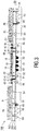
- Fig. 3 shows a cross-sectional view of a first embodiment of the device 100 of the invention.
- Fig. 4 shows the device 100 of this embodiment from the second side of the carrier substrate 20, on which side the contact pads 61-65 for external connection are present.
- Fig. 5 shows the device 100 of this embodiment from the first side of the carrier substrate 20, on which side the integrated circuit 10 is provided. It is observed that in Figs. 4 and 5 only parts of the substrate are shown; the substrate usually extends laterally, and the contact pads 63-65 generally form a closed ring around the integrated circuit.
- the embodiment thus is an example of a typical ball grid array package, as the skilled person will understand. Such a package is preferred, but the invention is not limited thereto.
- Fig. 5 the mechanical stiffner 29 is left out for reasons of clarity.
- Fig. 3 is not a true cross-section, as will be apparent from a comparison with Fig. 4 .
- the device as shown in Fig. 3 comprises an integrated circuit 10 and a carrier substrate 20.
- the carrier substrate 20 has a first side 21 and a second side 22. It comprises a body 20A of dielectric material and electrically conducting layers 20B, 20C on the first and second side 21, 22, respectively.
- the dielectric material in this case is an epoxy resin (FR-4) with a thickness of about 80 ⁇ m, and the electrically conducting materials are made of copper.
- the resolution of interconnects and other tracks defined in the copper is in the order of 50 ⁇ m, and there is a minimal distance between neighboring tracks of 100 ⁇ m, in this embodiment.
- On the first side 21 a mechanical stiffening layer 29 is present, which provides additional mechanical stability.
- the stiffening layer 29 has in this case a thickness of about 300 ⁇ m and is made of the same material as the body 20A.
- the integrated circuit 10 has a first side 18 on which bond pads 11 are provided (see Fig. 5 ).
- the bond pads 11 are connected via wirebonds 49 to the bond pads 41, 42, 43 on the first side 21 of the carrier substrate 20.
- These bond pads 41-43 are provided with an additional thickness as compared to the electrically conducting layer 20B, which additional thickness is meant for mechanical stability during the wirebonding and provided by electroplating in known manner.
- the integrated circuit in the invention is provided with core functionality and with peripheral functionality.
- separate areas are defined in the carrier substrate 20 for each of the functionalities: a core area 31 for the core functionality and a peripheral area 32 for the peripheral functionality.
- the peripheral area 32 is positioned laterally around the core area 31. This is preferred, but not necessary.
- Specific bond pads are present on the first side 21 of the carrier substrate 20 for the core functionality 42 and the peripheral functionality 43.
- the bond pads for the peripheral functionality 43 include the bond pads for signal transmission and voltage supply.
- the bond pads for the core functionality 42 include the bond pads for the voltage supply.
- there are bond pads for ground connections 41 which are common for the core and peripheral functionality.
- the bond pads for ground connection 41 and for voltage supply of the core functionality 42 are implemented in this embodiment as concentrical rings, with the ring for ground inside the ring for power.
- the core area 31 and the peripheral area 32 of the carrier substrate 20 are designed differently.
- the bond pads 41, 42 on the first side 21 are directly connected to the second side 22, so as to minimize inductive losses.
- the contact pads 61 for ground connection are positioned directly below the corresponding bond pads 41.
- the bond pads 41 for ground are interconnected through a ground plane 52 on the first side 21 of the carrier substrate 20.
- the contact pads 62 for voltage supply connection are coupled to the corresponding bond pads 42 through interconnects 67 on the second side 22 of the carrier substrate 20 to the vertical interconnects 66.
- each contact pad 62 for voltage supply connection is provided with a (non-shown) ESD protection structure.
- the center-four contact pads 62 are primarily meant for improvement of the thermal behavior of the package.
- the interconnects 53 end up at vertical interconnects 73, 75, as shown in Fig. 5 .
- the interconnects 75 correspond to the contact pads 65 intended for voltage supply connections of the peripheral functionality.
- the interconnects 73 correspond to the contact pads 63 used for signal transmission.
- the contact pads 64 for ground are positioned at the outer periphery of the contact pads array, generally a ball grid array. This provides some protection against electromagnetic inference.
- contact pads 65 meant for voltage supply connections could be used for ground connections. This is a matter of design and depends on the required number of voltage supply connections and ground connections to an external carrier. It is however preferred that the contact pads 63-65 are subdivided into subgroups 164, 165. In the subgroups 164,165 up to eight contact pads 63 for signal transmission are present around a center contact pad 64, 65 that is either a pad for ground or for voltage supply. In this manner a signal path and its signal return can be neighboring, and hence the distance between both is minimal. This enforces a proper transmission path for the carrier substrate 20 to an external carrier.
- Fig. 6 shows a cross-sectional view of a second embodiment of the device 100 of the invention.
- Fig. 7 shows the device 100 of this second embodiment from the second side of the carrier substrate 20, where the contact pads 61-65 for external connection are present.
- Fig. 8 shows the integrated circuit 10 of this second embodiment with its side 18 with bond pads 11-13. It is observed that in Fig. 7 only part of the substrate is shown; the substrate usually extends laterally, and the contact pads 63-65 generally form a closed ring around the integrated circuit.
- the embodiment is an example of a typical ball grid array package, as the skilled person will understand. Such a package is preferred, but the invention is not limited thereto.
- Fig. 6 is not a true cross section, as the skilled person will find out on comparison with Fig. 7 .
- the device 100 of this second embodiment is equal in many features to that of the first embodiment.
- the carrier substrate 20 is subdivided into a core area 31 and a peripheral area 32.
- the carrier substrate 20 is provided with a ground plane 51 on the second side 22 of the substrate, extending in the peripheral area 32, and with interconnects 53, that have a transmission line character. It is observed that in both cases the bond pads 43 for the peripheral functionality are provided near to the edge of the core area 31, such that the transmission lines are well defined and their behavior not negatively affected by bond wires or the like.
- the main difference between the first and the second embodiment resides in that the second embodiment is a flip-chip embodiment.
- This has substantial advantages. First of all, there is no need for an additional bond pad layer on the first side 21 of the carrier substrate 20, which is needed for the wirebonding. There is no need for a redistribution layer (i.e. through the interconnects 66, 67) or a staggered pad array either.
- the solder balls between the bond pads 11,12, 13 of the integrated circuit and the bond pads 41, 42, 43 at the carrier substrate 20 can be provided directly on the electrically conductive layer 20B.
- both contact pads 61,62, as well as the corresponding bond pads 41,42 and 11,12 are arranged in a 'chessboard'-pattern.
- each closest neighbor of a pad for voltage supply 12,42,62 is a pad for ground 11,41,61 and vice versa. Consequently, the ball grid array has a coaxial structure, with a reduction of the effective inductance of about 50%, and a lower ground bounce voltage.
- the bond pads 11,12 at the integrated circuit 10 are in this case provided in an inner area. These pads 11,12 demonstrate - seen in perpendicular projection on the substrate of the integrated circuit - an overlap with the active region.
- Such a design of bond pads is also known as bond pads on active areas (They may be provided on top of a passivation layer, in order to provide sufficient strength.
- the number of ESD protection structures can be reduced. In fact, they are needed only at the outer edge of the core area 31. This is based on the insight that the voltage gradient in the core area 31 shall be minimal during ESD stress, as a consequence of the good conductivity. For the ground connections, ESD protection structures are needed in the core area 31 and in the peripheral area 32.
- the thermal management of the device 100 can be improved in that a heat spreading layer 15 is provided on the first side 21 of the carrier substrate and the backside of the integrated circuit 10, e.g. the side facing away from the bond pads 11-13. It is particularly preferred that the semiconductor substrate of the integrated circuit 10 is thinned, thereby reducing the path of thermal resistance to the heat spreading layer 15.
- the electronic device 100 comprises a semiconductor device, particularly an integrated circuit 10 and a carrier substrate 20 with a bottom and top conductive layer, and is provided with voltage supply, ground and signal transmission connections.
- the integrated circuit 10 is subdivided into core functionality 110 and peripheral functionality 210, and the carrier substrate 20 is subdivided into a corresponding core area 31 and peripheral area 32.
- the ground connections of both core and periphery are mutually coupled through an interconnect 22 in the carrier substrate 20.
- This interconnect is particularly a ground plane, and allows the provision of a transmission line character to the interconnects for signal transmission for the periphery.
Landscapes
- Semiconductor Integrated Circuits (AREA)
- Internal Circuitry In Semiconductor Integrated Circuit Devices (AREA)
Claims (7)
- Elektronische Vorrichtung (100) mit:- mindestens einer Halbleitervorrichtung (10), die auf einer Seite mit einer Mehrzahl von Bondpads (11, 12, 13) versehen ist; und- einem Trägersubstrat (20), das eine Schicht elektrisch isolierenden Materials (20A) aufweist und eine erste Seite (21) und eine entgegengesetzte zweite Seite (22), die jeweils mit einer elektrisch leitenden Schicht (20B, 20C) versehen sind, auf deren ersten Seite Bondpads (41, 42, 43) vorliegen, die zum Koppeln an die Bondpads (11, 12, 13) der integrierten Schaltung (10) geeignet sind, und auf deren zweiten Seite Kontaktpads (61, 62, 63, 64, 65) zum externen Koppeln vorliegen, wobei die Kontaktpads (61, 62, 63, 64, 65) und die Bondpads (41, 42, 43) gemäß eines gewünschten Musters elektrisch miteinander verbunden sind, wobei ein erster Abschnitt der Kontaktpads (61, 64, 65) für einen Masseanschluss definiert ist, ein zweiter Abschnitt der Kontaktpads (62, 65) für einen Spannungsversorgungsanschluss definiert ist und ein dritter Abschnitt der Kontaktpads (63) für eine Signalübertragung definiert ist, wobei in der elektronischen Vorrichtung (100)- die mindestens eine Halbleitervorrichtung (10) mit einer Kernfunktionalität und einer peripheren Funktionalität vorgesehen ist, wobei die Kernfunktionalität und die periphere Funktionalität jeweils mit einem Spannungsversorgungsanschluss und einem Masseanschluss vorgesehen sind,- das Trägersubstrat (20) lateral in einen Kernbereich (31) und einen peripheren Bereich (32) unterteilt ist, wobei im Kernbereich (31) Kontaktpads (61, 62) für die Kernfunktionalität vorgesehen sind und im peripheren Bereich (32) Kontaktpads (63, 64, 65) für die periphere Funktionalität vorgesehen sind, wobei- das Trägersubtrat (20) mindestens eine Zwischenverbindung (51) aufweist, um den Masseanschluss der peripheren Funktionalität und den Masseanschluss der Kernfunktionalität miteinander zu verbinden, wobei- eine Massefläche (51) im peripheren Bereich (32) auf der zweiten Seite (22) des Trägersubstrats (20) definiert ist, wobei die Massefläche (51) die Zwischenverbindung zum beidseitigen Verbinden des Masseanschlusses der peripheren Funktionalität und des Masseanschlusses der Kernfunktionalität ist,- eine Massefläche (52) in dem Kernbereich (31) auf der ersten Seite (21) des Trägersubstrats (20) definiert ist und mit der Massefläche (51) im peripheren Bereich (32) durch vertikale Zwischenverbindungen (66) in dem Trägersubstrat (20) gekoppelt ist, und wobei- Mittel (111, 211) zum Entkoppeln der Spannungsversorgung der Kernfunktionalität und der peripheren Funktionalität an die gemeinsame Masse vorhanden sind, wobei- die Mittel (111, 211) zum Entkoppeln einen Entkopplungskondensator (211) in der peripheren Funktionalität aufweisen, der sich entweder in der mindestens einen Halbleitervorrichtung (10) befindet oder an der ersten Seite (21) des Trägersubstrats (20).
- Elektronische Vorrichtung (100) nach Anspruch 1, wobei- sich der periphere Bereich (32) um den Kernbereich (31) herum befindet;- Zwischenverbindungen (53) zwischen den Kontaktpads (63, 65) und den Bondpads (43) der peripheren Funktionalität auf der ersten Seite (21) des Trägersubstrats (20) definiert sind, wobei die Zwischenverbindungen einen Übertragungsleitungscharakter aufweisen.
- Elektronisch Vorrichtung (100) nach Anspruch 2, wobei die Kontaktpads (61, 62) in dem Kernbereich (31) in einem Array definiert sind, wobei die Pads für den Masseanschluss (61) und den Versorgungsanschluss (62) derart in dem Array angeordnet sind, dass jeder der Pads (61) für den Masseanschluss Pads (62) für Versorgungsanschlüsse als die nächstgelegenen Nachbarpads aufweist.
- Elektronische Vorrichtung (100) nach Anspruch 2, wobei die Kontaktpads (63, 64, 65) in dem peripheren Bereich in Untergruppen definiert sind, wobei jede Untergruppe einen Kontaktpad (65) für den Versorgungsanschluss aufweist oder einen Kontaktpad (64, 65) für den Masseanschluss und mehrere Kontaktpads (63) für die Signalübertragung, wobei alle Pads (63) für die Signalübertragung das Kontaktpad (64, 65) für entweder den Spannungsanschluss oder den Masseanschluss als einen benachbarten Pad aufweisen.
- Elektronische Vorrichtung (100) nach Anspruch 1 oder 2, wobei eine Versteifungsschicht (29) auf der ersten Seite (21) des Trägersubstrats (20) vorliegt, wodurch ein Teil der elektrisch leitenden Schicht (20B) bedeckt wird.
- Elektronisch Vorrichtung (100) nach Anspruch 1 oder 5, wobei die Halbleitervorrichtung (10) auf dem Trägersubstrat (20) in einer Flip-Chip-Ausrichtung angeordnet ist, wobei die Bondpads (41, 42, 43) an der Halbleitervorrichtung (10) und auf der ersten Seite (21) des Trägersubstrats (20) in einer entsprechenden Konfiguration positioniert sind, und wobei eine Wärmeausbreitungsschicht (15) auf der ersten Seite (21) des Trägersubstrats (20) vorgesehen ist und auf einer Seite der Halbleitervorrichtung, die von der Seite der Bondspads (41, 42, 43) abgewandt ist.
- Elektronische Vorrichtung (100) nach Anspruch 1, die ferner mit einem Versorgungsreiheninduktor (302) vorgesehen ist.
Priority Applications (1)
| Application Number | Priority Date | Filing Date | Title |
|---|---|---|---|
| EP04770150.3A EP1673807B1 (de) | 2003-10-10 | 2004-10-01 | Elektronisches bauteil |
Applications Claiming Priority (3)
| Application Number | Priority Date | Filing Date | Title |
|---|---|---|---|
| EP03103758 | 2003-10-10 | ||
| EP04770150.3A EP1673807B1 (de) | 2003-10-10 | 2004-10-01 | Elektronisches bauteil |
| PCT/IB2004/051945 WO2005036643A1 (en) | 2003-10-10 | 2004-10-01 | Electronic device and carrier substrate for same |
Publications (2)
| Publication Number | Publication Date |
|---|---|
| EP1673807A1 EP1673807A1 (de) | 2006-06-28 |
| EP1673807B1 true EP1673807B1 (de) | 2019-12-11 |
Family
ID=34429470
Family Applications (1)
| Application Number | Title | Priority Date | Filing Date |
|---|---|---|---|
| EP04770150.3A Expired - Lifetime EP1673807B1 (de) | 2003-10-10 | 2004-10-01 | Elektronisches bauteil |
Country Status (7)
| Country | Link |
|---|---|
| US (1) | US7253516B2 (de) |
| EP (1) | EP1673807B1 (de) |
| JP (1) | JP2007508688A (de) |
| KR (1) | KR101099925B1 (de) |
| CN (1) | CN100550365C (de) |
| TW (1) | TWI353663B (de) |
| WO (1) | WO2005036643A1 (de) |
Families Citing this family (18)
| Publication number | Priority date | Publication date | Assignee | Title |
|---|---|---|---|---|
| EP1673808B1 (de) * | 2003-10-10 | 2020-01-01 | Taiwan Semiconductor Manufacturing Co., Ltd. | Elektronisches bauteil und trägersubstrat |
| US7272802B2 (en) * | 2005-05-11 | 2007-09-18 | Lsi Corporation | R-cells containing CDM clamps |
| US8643163B2 (en) * | 2005-08-08 | 2014-02-04 | Stats Chippac Ltd. | Integrated circuit package-on-package stacking system and method of manufacture thereof |
| WO2007031298A1 (de) * | 2005-09-14 | 2007-03-22 | Htc Beteiligungs Gmbh | Flip-chip-modul und verfahren zum erzeugen eines flip-chip-moduls |
| US7518230B2 (en) * | 2005-12-14 | 2009-04-14 | Rohm Co., Ltd | Semiconductor chip and semiconductor device |
| US20080197474A1 (en) * | 2007-02-16 | 2008-08-21 | Advanced Chip Engineering Technology Inc. | Semiconductor device package with multi-chips and method of the same |
| US8946873B2 (en) * | 2007-08-28 | 2015-02-03 | Micron Technology, Inc. | Redistribution structures for microfeature workpieces |
| KR101006748B1 (ko) * | 2009-01-29 | 2011-01-10 | (주)인디링스 | 패드들의 동시 스위칭을 제어하는 고체 상태 디스크를 위한컨트롤러 |
| TWI452665B (zh) * | 2010-11-26 | 2014-09-11 | 矽品精密工業股份有限公司 | 具防靜電破壞及防電磁波干擾之封裝件及其製法 |
| US8628636B2 (en) * | 2012-01-13 | 2014-01-14 | Advance Materials Corporation | Method of manufacturing a package substrate |
| US9515017B2 (en) | 2014-12-18 | 2016-12-06 | Intel Corporation | Ground via clustering for crosstalk mitigation |
| JP6337867B2 (ja) * | 2015-10-26 | 2018-06-06 | 株式会社村田製作所 | 帯域通過型フィルタ及びデュプレクサ |
| EP3437129A4 (de) | 2016-03-30 | 2019-09-25 | INTEL Corporation | Hybride mikroelektronische substrate |
| US10734319B2 (en) * | 2017-10-06 | 2020-08-04 | Google Llc | Signal routing in integrated circuit packaging |
| MY208458A (en) * | 2019-09-26 | 2025-05-09 | Intel Corp | Organic mold interconnects in shielded interconnects frames for integrated-circuit packages |
| CN111224317B (zh) * | 2020-04-20 | 2021-03-19 | 深圳市汇顶科技股份有限公司 | 激光发射装置 |
| US11670578B2 (en) | 2020-06-02 | 2023-06-06 | Micron Technology, Inc. | Ball grid arrays and associated apparatuses and systems |
| US12288756B2 (en) | 2022-03-11 | 2025-04-29 | Chipletz, Inc. | Semiconductor package with integrated capacitors |
Citations (3)
| Publication number | Priority date | Publication date | Assignee | Title |
|---|---|---|---|---|
| US5258575A (en) * | 1990-05-07 | 1993-11-02 | Kyocera America, Inc. | Ceramic glass integrated circuit package with integral ground and power planes |
| JP2001168266A (ja) * | 1999-12-13 | 2001-06-22 | Hitachi Ltd | 半導体装置 |
| WO2001058224A1 (en) * | 2000-01-26 | 2001-08-09 | The Industree B.V. | Printed circuit board |
Family Cites Families (18)
| Publication number | Priority date | Publication date | Assignee | Title |
|---|---|---|---|---|
| US5741729A (en) * | 1994-07-11 | 1998-04-21 | Sun Microsystems, Inc. | Ball grid array package for an integrated circuit |
| EP0743929B1 (de) | 1994-12-12 | 1998-07-15 | Koninklijke Philips Electronics N.V. | Substrat aus einem keramischen material |
| AU4697496A (en) | 1995-01-24 | 1996-08-14 | Intel Corporation | High performance integrated circuit package |
| US5959320A (en) * | 1997-03-18 | 1999-09-28 | Lsi Logic Corporation | Semiconductor die having on-die de-coupling capacitance |
| JP3517112B2 (ja) * | 1998-04-27 | 2004-04-05 | 京セラ株式会社 | 配線基板 |
| JP3495917B2 (ja) * | 1998-07-15 | 2004-02-09 | 日本特殊陶業株式会社 | 多層配線基板 |
| JP3723688B2 (ja) * | 1998-07-23 | 2005-12-07 | 京セラ株式会社 | 配線基板 |
| DE19939483A1 (de) | 1999-08-20 | 2001-03-08 | Philips Corp Intellectual Pty | Passives Bauelement mit Verbundwerkstoff |
| US6509646B1 (en) * | 2000-05-22 | 2003-01-21 | Silicon Integrated Systems Corp. | Apparatus for reducing an electrical noise inside a ball grid array package |
| TW525417B (en) * | 2000-08-11 | 2003-03-21 | Ind Tech Res Inst | Composite through hole structure |
| US6448639B1 (en) * | 2000-09-18 | 2002-09-10 | Advanced Semiconductor Engineering, Inc. | Substrate having specific pad distribution |
| JP4613416B2 (ja) * | 2000-11-28 | 2011-01-19 | 日本電気株式会社 | 半導体装置およびその実装方法 |
| US6472747B2 (en) * | 2001-03-02 | 2002-10-29 | Qualcomm Incorporated | Mixed analog and digital integrated circuits |
| US6696763B2 (en) * | 2001-04-02 | 2004-02-24 | Via Technologies, Inc. | Solder ball allocation on a chip and method of the same |
| TW511414B (en) | 2001-04-19 | 2002-11-21 | Via Tech Inc | Data processing system and method, and control chip, and printed circuit board thereof |
| TW498472B (en) * | 2001-11-27 | 2002-08-11 | Via Tech Inc | Tape-BGA package and its manufacturing process |
| US6930381B1 (en) * | 2002-04-12 | 2005-08-16 | Apple Computer, Inc. | Wire bonding method and apparatus for integrated circuit |
| WO2004064151A2 (en) | 2003-01-13 | 2004-07-29 | Koninklijke Philips Electronics N.V. | Electronic device and method of manufacturing a substrate |
-
2004
- 2004-10-01 EP EP04770150.3A patent/EP1673807B1/de not_active Expired - Lifetime
- 2004-10-01 US US10/574,882 patent/US7253516B2/en not_active Expired - Lifetime
- 2004-10-01 CN CNB2004800294565A patent/CN100550365C/zh not_active Expired - Lifetime
- 2004-10-01 WO PCT/IB2004/051945 patent/WO2005036643A1/en not_active Ceased
- 2004-10-01 KR KR1020067006911A patent/KR101099925B1/ko not_active Expired - Lifetime
- 2004-10-01 JP JP2006530964A patent/JP2007508688A/ja active Pending
- 2004-10-07 TW TW093130419A patent/TWI353663B/zh not_active IP Right Cessation
Patent Citations (3)
| Publication number | Priority date | Publication date | Assignee | Title |
|---|---|---|---|---|
| US5258575A (en) * | 1990-05-07 | 1993-11-02 | Kyocera America, Inc. | Ceramic glass integrated circuit package with integral ground and power planes |
| JP2001168266A (ja) * | 1999-12-13 | 2001-06-22 | Hitachi Ltd | 半導体装置 |
| WO2001058224A1 (en) * | 2000-01-26 | 2001-08-09 | The Industree B.V. | Printed circuit board |
Also Published As
| Publication number | Publication date |
|---|---|
| US20070018287A1 (en) | 2007-01-25 |
| JP2007508688A (ja) | 2007-04-05 |
| US7253516B2 (en) | 2007-08-07 |
| CN100550365C (zh) | 2009-10-14 |
| TWI353663B (en) | 2011-12-01 |
| KR101099925B1 (ko) | 2011-12-28 |
| TW200518307A (en) | 2005-06-01 |
| WO2005036643A1 (en) | 2005-04-21 |
| EP1673807A1 (de) | 2006-06-28 |
| CN1864259A (zh) | 2006-11-15 |
| KR20060122826A (ko) | 2006-11-30 |
Similar Documents
| Publication | Publication Date | Title |
|---|---|---|
| US7253516B2 (en) | Electronic device and carrier substrate for same | |
| US7321166B2 (en) | Wiring board having connecting wiring between electrode plane and connecting pad | |
| EP1153419B1 (de) | Mehrchipgehäuse mit integrierten rf-fähigkeiten | |
| US7157794B2 (en) | Semiconductor device that suppresses variations in high frequency characteristics of circuit elements | |
| US20020140081A1 (en) | Highly integrated multi-layer circuit module having ceramic substrates with embedded passive devices | |
| US7795709B2 (en) | Shielding noisy conductors in integrated passive devices | |
| CN101009256A (zh) | 半导体装置 | |
| US7986532B2 (en) | Split thin film capacitor for multiple voltages | |
| EP1673808B1 (de) | Elektronisches bauteil und trägersubstrat | |
| US8547681B2 (en) | Decoupling capacitor | |
| WO2005074402A2 (en) | An integrated circuit | |
| CN111599799A (zh) | 集成电路 | |
| TW202247386A (zh) | 用於極高頻操作之覆晶球柵陣列型積體電路封裝 | |
| US20090085158A1 (en) | Package with improved connection of a decoupling capacitor | |
| US20050112842A1 (en) | Integrating passive components on spacer in stacked dies | |
| TWI833386B (zh) | 半導體封裝 | |
| US20090273079A1 (en) | Semiconductor package having passive component bumps |
Legal Events
| Date | Code | Title | Description |
|---|---|---|---|
| PUAI | Public reference made under article 153(3) epc to a published international application that has entered the european phase |
Free format text: ORIGINAL CODE: 0009012 |
|
| 17P | Request for examination filed |
Effective date: 20060510 |
|
| AK | Designated contracting states |
Kind code of ref document: A1 Designated state(s): AT BE BG CH CY CZ DE DK EE ES FI FR GB GR HU IE IT LI LU MC NL PL PT RO SE SI SK TR |
|
| DAX | Request for extension of the european patent (deleted) | ||
| RAP1 | Party data changed (applicant data changed or rights of an application transferred) |
Owner name: NXP B.V. |
|
| RAP1 | Party data changed (applicant data changed or rights of an application transferred) |
Owner name: TAIWAN SEMICONDUCTOR MANUFACTURING CO., LTD. |
|
| 17Q | First examination report despatched |
Effective date: 20150310 |
|
| STAA | Information on the status of an ep patent application or granted ep patent |
Free format text: STATUS: EXAMINATION IS IN PROGRESS |
|
| GRAP | Despatch of communication of intention to grant a patent |
Free format text: ORIGINAL CODE: EPIDOSNIGR1 |
|
| STAA | Information on the status of an ep patent application or granted ep patent |
Free format text: STATUS: GRANT OF PATENT IS INTENDED |
|
| INTG | Intention to grant announced |
Effective date: 20190506 |
|
| GRAS | Grant fee paid |
Free format text: ORIGINAL CODE: EPIDOSNIGR3 |
|
| GRAA | (expected) grant |
Free format text: ORIGINAL CODE: 0009210 |
|
| STAA | Information on the status of an ep patent application or granted ep patent |
Free format text: STATUS: THE PATENT HAS BEEN GRANTED |
|
| AK | Designated contracting states |
Kind code of ref document: B1 Designated state(s): AT BE BG CH CY CZ DE DK EE ES FI FR GB GR HU IE IT LI LU MC NL PL PT RO SE SI SK TR |
|
| REG | Reference to a national code |
Ref country code: GB Ref legal event code: FG4D |
|
| REG | Reference to a national code |
Ref country code: CH Ref legal event code: EP |
|
| REG | Reference to a national code |
Ref country code: AT Ref legal event code: REF Ref document number: 1213044 Country of ref document: AT Kind code of ref document: T Effective date: 20191215 |
|
| REG | Reference to a national code |
Ref country code: DE Ref legal event code: R096 Ref document number: 602004054412 Country of ref document: DE |
|
| REG | Reference to a national code |
Ref country code: IE Ref legal event code: FG4D |
|
| REG | Reference to a national code |
Ref country code: NL Ref legal event code: MP Effective date: 20191211 |
|
| PG25 | Lapsed in a contracting state [announced via postgrant information from national office to epo] |
Ref country code: SE Free format text: LAPSE BECAUSE OF FAILURE TO SUBMIT A TRANSLATION OF THE DESCRIPTION OR TO PAY THE FEE WITHIN THE PRESCRIBED TIME-LIMIT Effective date: 20191211 Ref country code: ES Free format text: LAPSE BECAUSE OF FAILURE TO SUBMIT A TRANSLATION OF THE DESCRIPTION OR TO PAY THE FEE WITHIN THE PRESCRIBED TIME-LIMIT Effective date: 20191211 Ref country code: BG Free format text: LAPSE BECAUSE OF FAILURE TO SUBMIT A TRANSLATION OF THE DESCRIPTION OR TO PAY THE FEE WITHIN THE PRESCRIBED TIME-LIMIT Effective date: 20200311 Ref country code: FI Free format text: LAPSE BECAUSE OF FAILURE TO SUBMIT A TRANSLATION OF THE DESCRIPTION OR TO PAY THE FEE WITHIN THE PRESCRIBED TIME-LIMIT Effective date: 20191211 Ref country code: GR Free format text: LAPSE BECAUSE OF FAILURE TO SUBMIT A TRANSLATION OF THE DESCRIPTION OR TO PAY THE FEE WITHIN THE PRESCRIBED TIME-LIMIT Effective date: 20200312 |
|
| PG25 | Lapsed in a contracting state [announced via postgrant information from national office to epo] |
Ref country code: CZ Free format text: LAPSE BECAUSE OF FAILURE TO SUBMIT A TRANSLATION OF THE DESCRIPTION OR TO PAY THE FEE WITHIN THE PRESCRIBED TIME-LIMIT Effective date: 20191211 Ref country code: RO Free format text: LAPSE BECAUSE OF FAILURE TO SUBMIT A TRANSLATION OF THE DESCRIPTION OR TO PAY THE FEE WITHIN THE PRESCRIBED TIME-LIMIT Effective date: 20191211 Ref country code: NL Free format text: LAPSE BECAUSE OF FAILURE TO SUBMIT A TRANSLATION OF THE DESCRIPTION OR TO PAY THE FEE WITHIN THE PRESCRIBED TIME-LIMIT Effective date: 20191211 Ref country code: PT Free format text: LAPSE BECAUSE OF FAILURE TO SUBMIT A TRANSLATION OF THE DESCRIPTION OR TO PAY THE FEE WITHIN THE PRESCRIBED TIME-LIMIT Effective date: 20200506 Ref country code: EE Free format text: LAPSE BECAUSE OF FAILURE TO SUBMIT A TRANSLATION OF THE DESCRIPTION OR TO PAY THE FEE WITHIN THE PRESCRIBED TIME-LIMIT Effective date: 20191211 |
|
| PG25 | Lapsed in a contracting state [announced via postgrant information from national office to epo] |
Ref country code: SK Free format text: LAPSE BECAUSE OF FAILURE TO SUBMIT A TRANSLATION OF THE DESCRIPTION OR TO PAY THE FEE WITHIN THE PRESCRIBED TIME-LIMIT Effective date: 20191211 |
|
| REG | Reference to a national code |
Ref country code: DE Ref legal event code: R097 Ref document number: 602004054412 Country of ref document: DE |
|
| REG | Reference to a national code |
Ref country code: AT Ref legal event code: MK05 Ref document number: 1213044 Country of ref document: AT Kind code of ref document: T Effective date: 20191211 |
|
| PLBE | No opposition filed within time limit |
Free format text: ORIGINAL CODE: 0009261 |
|
| STAA | Information on the status of an ep patent application or granted ep patent |
Free format text: STATUS: NO OPPOSITION FILED WITHIN TIME LIMIT |
|
| PG25 | Lapsed in a contracting state [announced via postgrant information from national office to epo] |
Ref country code: DK Free format text: LAPSE BECAUSE OF FAILURE TO SUBMIT A TRANSLATION OF THE DESCRIPTION OR TO PAY THE FEE WITHIN THE PRESCRIBED TIME-LIMIT Effective date: 20191211 |
|
| 26N | No opposition filed |
Effective date: 20200914 |
|
| PG25 | Lapsed in a contracting state [announced via postgrant information from national office to epo] |
Ref country code: AT Free format text: LAPSE BECAUSE OF FAILURE TO SUBMIT A TRANSLATION OF THE DESCRIPTION OR TO PAY THE FEE WITHIN THE PRESCRIBED TIME-LIMIT Effective date: 20191211 Ref country code: SI Free format text: LAPSE BECAUSE OF FAILURE TO SUBMIT A TRANSLATION OF THE DESCRIPTION OR TO PAY THE FEE WITHIN THE PRESCRIBED TIME-LIMIT Effective date: 20191211 Ref country code: PL Free format text: LAPSE BECAUSE OF FAILURE TO SUBMIT A TRANSLATION OF THE DESCRIPTION OR TO PAY THE FEE WITHIN THE PRESCRIBED TIME-LIMIT Effective date: 20191211 |
|
| PG25 | Lapsed in a contracting state [announced via postgrant information from national office to epo] |
Ref country code: IT Free format text: LAPSE BECAUSE OF FAILURE TO SUBMIT A TRANSLATION OF THE DESCRIPTION OR TO PAY THE FEE WITHIN THE PRESCRIBED TIME-LIMIT Effective date: 20191211 |
|
| REG | Reference to a national code |
Ref country code: CH Ref legal event code: PL |
|
| GBPC | Gb: european patent ceased through non-payment of renewal fee |
Effective date: 20201001 |
|
| PG25 | Lapsed in a contracting state [announced via postgrant information from national office to epo] |
Ref country code: MC Free format text: LAPSE BECAUSE OF FAILURE TO SUBMIT A TRANSLATION OF THE DESCRIPTION OR TO PAY THE FEE WITHIN THE PRESCRIBED TIME-LIMIT Effective date: 20191211 Ref country code: LU Free format text: LAPSE BECAUSE OF NON-PAYMENT OF DUE FEES Effective date: 20201001 |
|
| REG | Reference to a national code |
Ref country code: BE Ref legal event code: MM Effective date: 20201031 |
|
| PG25 | Lapsed in a contracting state [announced via postgrant information from national office to epo] |
Ref country code: BE Free format text: LAPSE BECAUSE OF NON-PAYMENT OF DUE FEES Effective date: 20201031 Ref country code: CH Free format text: LAPSE BECAUSE OF NON-PAYMENT OF DUE FEES Effective date: 20201031 Ref country code: GB Free format text: LAPSE BECAUSE OF NON-PAYMENT OF DUE FEES Effective date: 20201001 Ref country code: LI Free format text: LAPSE BECAUSE OF NON-PAYMENT OF DUE FEES Effective date: 20201031 |
|
| PG25 | Lapsed in a contracting state [announced via postgrant information from national office to epo] |
Ref country code: IE Free format text: LAPSE BECAUSE OF NON-PAYMENT OF DUE FEES Effective date: 20201001 |
|
| PG25 | Lapsed in a contracting state [announced via postgrant information from national office to epo] |
Ref country code: TR Free format text: LAPSE BECAUSE OF FAILURE TO SUBMIT A TRANSLATION OF THE DESCRIPTION OR TO PAY THE FEE WITHIN THE PRESCRIBED TIME-LIMIT Effective date: 20191211 Ref country code: CY Free format text: LAPSE BECAUSE OF FAILURE TO SUBMIT A TRANSLATION OF THE DESCRIPTION OR TO PAY THE FEE WITHIN THE PRESCRIBED TIME-LIMIT Effective date: 20191211 |
|
| PGFP | Annual fee paid to national office [announced via postgrant information from national office to epo] |
Ref country code: FR Payment date: 20231025 Year of fee payment: 20 Ref country code: DE Payment date: 20231027 Year of fee payment: 20 |
|
| REG | Reference to a national code |
Ref country code: DE Ref legal event code: R071 Ref document number: 602004054412 Country of ref document: DE |