EP1675149A2 - Ecran plat - Google Patents
Ecran plat Download PDFInfo
- Publication number
- EP1675149A2 EP1675149A2 EP05258071A EP05258071A EP1675149A2 EP 1675149 A2 EP1675149 A2 EP 1675149A2 EP 05258071 A EP05258071 A EP 05258071A EP 05258071 A EP05258071 A EP 05258071A EP 1675149 A2 EP1675149 A2 EP 1675149A2
- Authority
- EP
- European Patent Office
- Prior art keywords
- thermally conductive
- flat display
- frame
- display panel
- display apparatus
- Prior art date
- Legal status (The legal status is an assumption and is not a legal conclusion. Google has not performed a legal analysis and makes no representation as to the accuracy of the status listed.)
- Granted
Links
- 239000006260 foam Substances 0.000 claims description 9
- JOYRKODLDBILNP-UHFFFAOYSA-N Ethyl urethane Chemical compound CCOC(N)=O JOYRKODLDBILNP-UHFFFAOYSA-N 0.000 claims description 7
- 239000004088 foaming agent Substances 0.000 claims description 5
- 239000002210 silicon-based material Substances 0.000 claims description 4
- 239000003795 chemical substances by application Substances 0.000 claims description 2
- 239000000758 substrate Substances 0.000 description 19
- 239000010410 layer Substances 0.000 description 15
- 230000015572 biosynthetic process Effects 0.000 description 6
- 238000004519 manufacturing process Methods 0.000 description 6
- 239000000853 adhesive Substances 0.000 description 5
- 230000001070 adhesive effect Effects 0.000 description 5
- XUIMIQQOPSSXEZ-UHFFFAOYSA-N Silicon Chemical compound [Si] XUIMIQQOPSSXEZ-UHFFFAOYSA-N 0.000 description 4
- 229910052710 silicon Inorganic materials 0.000 description 4
- 239000010703 silicon Substances 0.000 description 4
- 239000000126 substance Substances 0.000 description 4
- 239000011521 glass Substances 0.000 description 3
- 229910052751 metal Inorganic materials 0.000 description 3
- 239000002184 metal Substances 0.000 description 3
- 230000005855 radiation Effects 0.000 description 3
- CPLXHLVBOLITMK-UHFFFAOYSA-N magnesium oxide Inorganic materials [Mg]=O CPLXHLVBOLITMK-UHFFFAOYSA-N 0.000 description 2
- 239000000395 magnesium oxide Substances 0.000 description 2
- AXZKOIWUVFPNLO-UHFFFAOYSA-N magnesium;oxygen(2-) Chemical compound [O-2].[Mg+2] AXZKOIWUVFPNLO-UHFFFAOYSA-N 0.000 description 2
- 239000000463 material Substances 0.000 description 2
- 238000000034 method Methods 0.000 description 2
- 238000012986 modification Methods 0.000 description 2
- 230000004048 modification Effects 0.000 description 2
- 239000011148 porous material Substances 0.000 description 2
- -1 Acryl Chemical group 0.000 description 1
- OAICVXFJPJFONN-UHFFFAOYSA-N Phosphorus Chemical compound [P] OAICVXFJPJFONN-UHFFFAOYSA-N 0.000 description 1
- 230000003247 decreasing effect Effects 0.000 description 1
- 238000007599 discharging Methods 0.000 description 1
- 238000005401 electroluminescence Methods 0.000 description 1
- AMGQUBHHOARCQH-UHFFFAOYSA-N indium;oxotin Chemical compound [In].[Sn]=O AMGQUBHHOARCQH-UHFFFAOYSA-N 0.000 description 1
- 239000011261 inert gas Substances 0.000 description 1
- 230000001788 irregular Effects 0.000 description 1
- 239000004973 liquid crystal related substance Substances 0.000 description 1
- 239000007937 lozenge Substances 0.000 description 1
- 239000011241 protective layer Substances 0.000 description 1
- 230000035939 shock Effects 0.000 description 1
- 239000005361 soda-lime glass Substances 0.000 description 1
Images




Classifications
-
- H—ELECTRICITY
- H05—ELECTRIC TECHNIQUES NOT OTHERWISE PROVIDED FOR
- H05K—PRINTED CIRCUITS; CASINGS OR CONSTRUCTIONAL DETAILS OF ELECTRIC APPARATUS; MANUFACTURE OF ASSEMBLAGES OF ELECTRICAL COMPONENTS
- H05K7/00—Constructional details common to different types of electric apparatus
- H05K7/20—Modifications to facilitate cooling, ventilating, or heating
- H05K7/20954—Modifications to facilitate cooling, ventilating, or heating for display panels
- H05K7/20963—Heat transfer by conduction from internal heat source to heat radiating structure
-
- H—ELECTRICITY
- H01—ELECTRIC ELEMENTS
- H01J—ELECTRIC DISCHARGE TUBES OR DISCHARGE LAMPS
- H01J2217/00—Gas-filled discharge tubes
- H01J2217/38—Cold-cathode tubes
- H01J2217/49—Display panels, e.g. not making use of alternating current
- H01J2217/492—Details
Definitions
- the present invention relates to a flat display apparatus. It more particularly relates to a flat display apparatus which can prevent a misdischarge and enhance the productivity.
- the plasma display is a device in which, when an inert gas located between a soda-lime glass front substrate and a rear substrate is discharged by a highfrequency voltage, vacuum ultraviolet radiation is generated, so that a fluorescent substance or phosphor coated therein emits visible light to display the image.
- Fig. 1 is a view showing schematically a structure of a background art plasma display apparatus.
- the plasma display comprises a case 110 including a front cabinet 111 and a back cover 112; a plasma display panel 120 for exciting the fluorescent substance; a driving unit 130 including a printed circuit board for driving and controlling the plasma display panel; a frame 140 connected to the driving unit for radiating heat generated when the plasma display apparatus is operated and for supporting the plasma display panel; and a thermally conductive sheet 150 formed between the plasma display panel and the frame for transmitting heat generated at the plasma display panel to the frame.
- the plasma display also includes a filter 160 formed by adhering a film on a transparent glass substrate and provided at a front side of the plasma display panel at a predetermined interval; a finger spring gasket 170 supporting the filter and electrically connecting the metal back cover and the filter; and a module supporter 190 supporting the plasma display apparatus including a filter supporter 180 and a driving apparatus.
- a front substrate 200 and a rear substrate 210 are combined in parallel with each other at a predetermined interval.
- the front substrate is formed by arranging a plurality of sustain electrode pairs, each of which includes a scan electrode 202 and a sustain electrode 203, on a front glass 201 which is a display surface on which the image is displayed.
- the rear substrate 210 is formed by arranging a plurality of address electrodes 213 on a rear glass 211 acting as a rear surface. The address electrodes 213 and the plurality of sustain electrode pairs 202, 203 cross each other.
- the scan electrode 202 and the sustain electrode 203 each comprise a pair of electrodes.
- Each of the pair of electrodes comprises a transparent electrode (a) made of transparent ITO (indium tin oxide) and a bus electrode (b) made of a metal.
- the scan electrode 202 and the sustain electrode 203 limit the discharge current and are covered with one or more upper dielectric layers 204 which insulate the electrode pair.
- a protective layer 205 on which magnesium oxide (MgO) is deposited is formed on an upper surface of the dielectric layer 204 for easily discharging.
- stripe type (or well type) walls 212 are disposed parallel with each other for forming a plurality of discharge spaces (that is, a plurality of discharge cells). Also, a plurality address electrodes 213 which perform the address discharge to generate vacuum ultraviolet radiation are disposed parallel with the walls 212.
- An upper surface of the rear substrate 210 is coated with red, green and blue (R,G,B) fluorescent substances 214 emitting visible radiation for displaying an image when the address discharge is generated.
- R,G,B red, green and blue
- a lower dielectric layer 215 is formed between the address electrodes 213 and the fluorescent substances 214 for protecting the address electrodes 213.
- a thermally conductive sheet is formed on a rear surface of the plasma display panel for transmitting heat generated from the plasma display panel, as shown in Fig. 3.
- the background art thermally conductive sheet 310 is formed on a frame 320, and then is adhered to a plasma display panel 330 having a front substrate 331 and a rear sheet 332.
- the thermally conductive sheet 310 makes the frame 320 adhere to the plasma display panel 330, and transmits the generated heat toward the frame 320 when the plasma display panel 330 is operated.
- the frame 320 is adhered to the plasma display panel 330 by the thermally conductive sheet 310 to support the thermally conductive sheet 310 and radiate heat transmitted through the thermally conductive sheet 310 toward the outside.
- the background art thermally conductive sheet is formed with a single sheet, and there is a drawback that the workability becomes lower. That is, when the frame is adhered to the plasma display panel by the single thermally conductive sheet, due to a large surface area of the thermally conductive sheet, an adhesive density between the thermally conductive sheet and the plasma display panel is reduced to lower the workability. If the adhesive density between the thermally conductive sheet and the plasma display panel is reduced as described above, an air layer is partially formed between the thermally conductive sheet and the plasma display panel. Such an air layer reduces the thermal conductivity, and therefore heat generated when the plasma display panel is operated cannot be radiated effectively.
- the present invention seeks to provide an improved flat display apparatus.
- Embodiments of the present invention can provide a flat display apparatus which has an improved structure to enhance the workability.
- Embodiments of the present invention can provide a flat display apparatus which reduces the manufacturing cost.
- Embodiments of the present invention can provide a flat display apparatus which can suppress a temperature gradient of the flat display panel.
- a flat display apparatus comprises a display panel; a frame provided at a rear surface of the display panel; and at least two thermally conductive sheets located between the display panel and the frame, the thermally conductive sheets being side-by-side and spaced apart from each other.
- a flat display apparatus comprises a display panel; a frame provided at a rear surface of the display panel; and at least two thermally conductive porous sheets located between the display panel and the frame, the thermally conductive porous sheets being side-by-side and spaced apart from each other, wherein the spacing between the thermally conductive porous sheets is 0.1 mm to 5.0 mm.
- a flat display apparatus comprises a display panel; a frame provided at a rear surface of the display panel, a first region of the frame having one or more holes therein; and a thermally conductive sheet located between the display panel and the frame, wherein the thermally conductive sheet is located at the first region of the frame.
- Embodiments of the present invention can enhance the workability by improving a structure of the flat display apparatus. Also, embodiments of the present invention can be advantageous in that manufacturing cost can be reduced by improving a structure of the flat display apparatus. In addition, the temperature gradient of a flat display panel can be suppressed.
- a flat display apparatus in accordance with another aspect of the invention, includes a display panel, a frame provided on a rear surface of the display panel, and at least two thermally conductive sheets formed between the display panel and the frame.
- the thermally conductive sheets may be spaced apart from each other at predetermined distances.
- the thermally conductive sheets are smaller in size than the display panel, so that edges of the thermally conductive sheets are spaced from an edge of the display panel.
- the distance between the thermally conductive sheets is 0.1 mm to 5.0 mm.
- the thermally conductive sheets have a thickness of 0.1 mm to 2.0 mm.
- the thermally conductive sheets are arranged in a longitudinal direction or a widthwise direction of the frame.
- the thermally conductive sheet is a porous pad or porous sheet.
- the porous sheet may contain a foaming agent, such as urethane foam.
- the porous pad or the porous sheet may contain silicon material.
- the frame, the thermally conductive sheets and the frame may have one or more holes formed thereon.
- a flat display apparatus in accordance with another aspect of the invention, includes a display panel, a frame provided on a rear surface of the display panel, and two or more thermally conductive sheets placed between the display panel and the frame.
- the thermally conductive sheets are spaced apart from each other at a distance of approximately 0.1mm to 5.0 mm.
- a flat display apparatus in accordance with another aspect of the invention, includes a display panel, a frame provided on a rear surface of the display panel, and a thermally conductive sheet formed between the display panel and the frame.
- the frame has one or more holes formed thereon.
- the thermally conductive sheet may be a porous pad or a porous sheet containing a foam agent.
- the holes may be disposed regularly or irregularly on the frame. In one embodiment, each hole formed on the frame has a size of approximately 0.1 mm to 10.0 mm.
- the holes may be formed on a section of the frame on which the thermally conductive sheet is placed.
- the thermally conductive sheet may have one or more holes formed thereon, having a diameter of approximately 0.1 mm to 5.0 mm. The holes formed on the thermally conductive sheet may correspond to the holes formed on the frame.
- Fig. 1 is a view showing schematically a structure of the background art plasma display apparatus
- Fig. 2 is a view showing the background art plasma display apparatus.
- Fig. 3 is a view showing schematically a thermally conductive sheet in the background art plasma display apparatus.
- Fig. 4 is a view showing schematically a thermally conductive sheet in a plasma display apparatus according to the first embodiment of the present invention.
- Fig. 5 is a view showing schematically a modified structure of the flat display apparatus according to the first embodiment of the present invention.
- Fig. 6 is a view showing schematically a frame according to the first embodiment of the present invention.
- Fig. 7 is a view showing schematically another modified structure of the flat display apparatus according to the first embodiment of the present invention.
- Fig. 8a and Fig. 8b are views for illustrating a structure of the flat display apparatus according to the second embodiment of the present invention.
- Fig. 9a and Fig. 9b are graphs for illustrating the thermal characteristic of the flat display panel according to the second embodiment of the present invention.
- a thermally conductive sheet 430 of the flat display apparatus is formed on a frame 420, and then adhered to a rear surface of a flat display panel 410.
- the flat display panel 410 includes a front substrate 411 of a flat display apparatus such as a PDP, an LCD and the like, and a rear substrate 412. An image is displayed on the flat display panel 410 when the flat display apparatus is operated.
- the frame 420 supports the flat display panel 410 and radiates heat generated by the flat display panel 410 toward an outside when the apparatus is operated.
- the thermally conductive sheet 430 acts as a medium which transmits heat generated by the flat display panel 410 toward the frame 420 when the apparatus is operated.
- the thermally conductive sheet 430 is formed of at least two unit sheets which are spaced from each other at a particular distance.
- the formation of an air layer between the frame 420 and the thermally conductive sheets 430 can be effectively suppressed.
- the thermally conductive sheet is attached to the frame in the state where the thermally conductive sheet is not aligned with the frame, the entire thermally conductive sheet needs to be removed from the frame.
- the thermally conductive sheets 430 are attached to the frame 420 in the state where one of the thermally conductive sheets 430 is not aligned with the frame 420, only the thermally conductive sheet 430 which is not aligned with the frame 420 needs to be removed. Therefore, the workability is made easier, and it is possible to reduce a loss of the thermally conductive sheet 430 caused by an inferior alignment state, so that manufacturing costs can be reduced.
- Each edge of the thermally conductive sheets 430 attached to the frame 420 is located inside of a corresponding edge of the flat display panel 410 at a particular gap.
- the flat display panel 410 has margins formed on an upper edge section, a lower edge section and both side edge sections thereof, a sufficient tolerance can be obtained when the thermally conductive sheets 430 attached to the frame 420 are attached to the flat display panel 410, so that the workability can be enhanced.
- a detailed description of a distance between the thermally conductive sheets 430 according to a feature of the present invention as above will be described below with reference to the second embodiment.
- the thermally conductive sheets 430 may have a thickness of approximately 0.1 mm to 2.0 mm.
- the thickness of 0.1 mm of the thermally conductive sheets 430 is a minimum thickness for forming a sheet shape, and if the thickness exceeds 2 mm, the thermal conductivity is lowered so that the thermally conductive sheets 430 cannot sufficiently radiate the generated heat toward the outside of the frame 420 when the flat display apparatus 410 is operated.
- the two or more thermally conductive sheets 430 are attached to the frame 420 in one of a longitudinal direction or a widthwise direction of the frame 420.
- the thermally conductive sheets 430 can be made of metal with a high thermal conductivity; however, it is preferable to use a thermally conductive tape or silicon and the like for convenience of the assembly process.
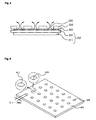
- Fig. 5 is a view schematically showing another structure of the flat display apparatus according to the first embodiment, wherein a thermally conductive sheet 530 is formed on a frame 520, and then adhered to a rear surface of a flat display panel 510.
- the flat display panel 510 includes a front substrate 511 of a flat display apparatus such as a PDP, an LCD and the like, and a rear substrate 512. An image is displayed on the flat display panel 510 when the flat display apparatus is operated.
- the frame 520 supports the flat display panel 510 and radiates heat generated at the flat display panel 510 toward an outside when the apparatus is operated.
- One surface of the thermally conductive sheet 530 is attached to the frame 520 and the other is attached to the flat display panel 510.
- the thermally conductive sheet 530 acts as a medium which transmits heat generated at the flat display panel 510 toward the frame 520 when the apparatus is operated.
- the frame 520 has one or more holes 540 formed thereon.
- the holes 540 of the frame are formed on a section on which the thermally conductive sheet 530 is formed.
- a porous pad or a porous sheet is preferably used as the thermally conductive sheet 530 so as to enable air remaining between the flat display panel 510 and the thermally conductive sheet 530 to flow toward the frame 520 through the thermally conductive sheet 530. Since the porous pad or the porous sheet or the porous sheet makes the remaining air pass toward the frame 520 and absorbs noise and vibration, the porous pad or the porous sheet prevents the noise and vibration generated when the flat display panel 510 is operated from being transmitted to the frame 520. In order to absorb the noise and vibration generated in the flat display panel 510, the porous pad or the porous sheet is made of porous material with a low density and a low hardness.
- the porous pad may be made by mixing urethane foam with silicon material and then applying an adhesive on front and rear surfaces of the manufactured pad, so that the porous pad or the porous sheet is obtained.
- a plurality of porosities are formed in the silicon of the pad.
- Acryl material may be used as the adhesive applied on the front and rear surfaces of the pad.
- a content rate of the silicon is approximately 89%
- a content rate of the urethane foam is approximately 10%
- a content rate of the adhesive is approximately 1%.
- a frame 600 according to the first embodiment has a plurality of holes 610 formed thereon.
- an air layer is not just formed on specific areas, but is formed irregularly on the entire surface.
- the holes 610 are formed on a section of the frame 600 on which the thermally conductive sheet 530 is formed. At this time, the holes 610 are disposed regularly at regular intervals or disposed irregularly on the frame 600.
- each hole 610 of the frame 600 can be any one of a circular shape 611, an elliptical shape, a rectangular shape 612 or a lozenge shape. That is, it is possible to modify the shape of the holes 610 of the frame 600 according to the convenience and need of the manufacturer.
- the size (diameter or height/width) of the hole 610 is greater than 0.1 mm, taking a processing tolerance into consideration, and is less than 10.0 mm, taking into consideration the mechanical strength and heat-radiating efficiency of the frame 600.
- Fig. 7 is a view schematically showing another structure of the flat display apparatus according to the first embodiment, wherein a thermally conductive sheet 730 is formed on a frame 720, and then adhered to a rear surface of a flat display panel 710.
- the flat display panel 710 includes a front substrate 711 of the general flat display apparatus such as the PDP, the LCD and the like, and a rear substrate 712. An image is displayed on the flat display panel when the flat display apparatus is operated.
- a frame 720 supports the flat display panel 710 and radiates heat generated at the flat display panel 710 toward an outside when the apparatus is operated.
- thermally conductive sheet 730 One surface of the thermally conductive sheet 730 is attached to the frame 720 and the other is attached to the flat display panel 710, so that the thermally conductive sheet 730 acts as a medium which transmits heat generated at the flat display panel 710 toward the frame 720 when the apparatus is operated.
- thermally conductive sheet 730 has one or more holes 740 formed thereon, and at least one or more holes 750 are formed on the frame 720.
- the holes 740 formed on the thermally conductive sheet 730 are matched with the holes 750 formed on the frame 720, respectively.
- the remaining air is exhausted through the holes 740 of the thermally conductive sheet 730 and the holes 750 of the frame 720 matched with the holes 740 of the thermally conductive sheet 730 when the thermally conductive sheet 730 is attached to the flat display panel 710.
- thermally conductive sheet 730 is made of the porous material so that air can be effectively exhausted through the thermally conductive sheet 730 itself and the holes 740 of the thermally conductive sheet 730.
- the size (diameter or width/height) of each hole 740 of the thermally conductive sheet 730 is 0.1 mm to 5.0 mm.
- the minimum size of a hole 740 is 0.1 mm, taking into consideration the processing tolerance, and 5.0 mm is a maximum size of a hole 740, taking into consideration that the thermally conductive sheet 730 at a portion on which the hole 740 is formed is decreased.
- a size (diameter or width X height) of each hole 750 of the frame is 0.1 mm or more, taking into consideration the processing tolerance, and is 10.0 mm or less, taking into consideration a mechanical strength and a heat radiating-efficiency of the frame 720.
- the number of holes 750 of the frame 720 is preferably the same as the number of holes 740 of the thermally conductive sheet 730, and so an efficiency of the frame 720 can be increased.
- a support bracket (not shown) and a mount (not shown) may be provided on a rear surface of the frame 720 for supporting and fixing the flat display apparatus.
- the formation of an air layer can be suppressed by forming the holes 750 at a section of the frame 720 adjacent to a section on which it is difficult to form the hole.
- a thermally conductive sheet 830 of a flat display apparatus is formed on a frame 820, and then adhered to a rear surface of a flat display panel 810.
- the flat display panel 810 includes a front substrate 811 of the general flat display apparatus such as a PDP, an LCD and the like, and a rear substrate 812. An image is displayed on the flat display panel 810 when the flat display apparatus is operated.
- the frame 820 supports the flat display panel 810 and radiates heat generated at the flat display panel 810 toward an outside when the apparatus is operated.
- thermally conductive sheet 830 acts as a medium which transmits heat generated by the flat display panel 810 toward the frame 820 when the apparatus is operated.
- the thermally conductive sheet 830 contains a plurality of sheets, which are spaced apart from each other at certain distances.
- thermally conductive sheets 830 When two or more thermally conductive sheets 830 are formed at certain distances, the workability is enhanced, the formation of an air layer is suppressed and manufacturing cost is reduced. The description is omitted since the description thereof has been set forth above regarding the first embodiment.
- a width of the space section 840 between the thermally conductive sheets 830 is 0.1 mm to 5.0 mm.
- a minimum distance of 0.1 mm takes into consideration the processing tolerance, and a maximum distance of 5.0 mm is an distance at which the misdischarge caused by the temperature gradient of the flat display panel 810 can be prevented.
- the thermally conductive sheets 830 are formed such that the distance between an edge of the each thermally conductive sheet 830 and an edge of the flat display panel 810 is 0.1 mm to 5.0 mm.
- a minimum distance of 0.1 mm takes into consideration the processing tolerance, and a maximum distance of 5.0 mm is a distance at which the misdischarge caused by the temperature gradient of the flat display panel 810 can be prevented.
- the distance between an edge of the each thermally conductive sheet 830 and an edge of the display area of the flat display panel on which an image display is displayed when the flat display apparatus is operated is 5 mm or less.
- the thickness of the thermally conductive sheet 830 is, in the present non-limiting embodiment, 0.1 mm to 2.0 mm, and the misdischarge caused by the temperature gradient is not generated in the flat display panel 890 when the space section 840 between the thermally conductive sheets 830 is 5.0 mm or less. That is, relating to a width of the space section 840 between the thermally conductive sheets 830, a thickness of the thermally conductive sheet 830 acts as a factor which influences the temperature gradient. A minimum thickness of 0.1 mm takes into consideration the processing tolerance, and 5.0 mm is a maximum thickness at which an acceptable temperature gradient is generated. The thermal conductivity of the entire thermally conductive sheet 830 with a thickness of 2 mm is significantly reduced, thus a temperature gradient is generated if the width of the space section 840 between the thermally conductive sheets 830 is 5.0 mm or less.
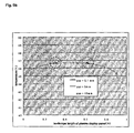
- Fig. 9a and Fig. 9b are graphs for illustrating the thermal characteristic of the flat display panel according to the second embodiment.
- the x axis in Fig. 9a indicates each position in a widthwise direction of the flat display panel, and the y axis indicates a temperature measured at each position of the flat display panel.
- Two thermally conductive sheets 830 are formed on the frame 820, and a certain distance between the two thermally conductive sheets 830 is formed at a section from which the zero point is spaced apart at 0.35 m.
- the curves indicate changes of the temperature at the position at which the distance between the thermally conductive sheets is 0.1 mm, 5.0 mm and 10.0 mm, respectively.
- the x axis in Fig. 9b indicates each position in a widthwise direction of the flat display panel, and the y axis indicates the temperature measured at each position of the flat display panel.
- Three thermally conductive sheets 830 are formed on the frame, and certain distances between two thermally conductive sheets 830 are formed at a section from which the zero point is spaced apart at 0.35 m and 0.65 m.
- the curves indicate changes of the temperature at the position at which the distance between the thermally conductive sheets is 0.1 mm, 5.0 mm and 10.0 mm, respectively.
- the temperature at a section of the flat display panel corresponding to the distance between the thermally conductive sheets is increased.
- the distance between the thermally conductive sheets is 5.0 mm or less, a misdischarge caused by a temperature gradient is not generated.
- the thermally conductive sheet is placed between the flat display panel and the frame, the thermally conductive sheet is divided into two or more sheets, and a distance is formed between the thermally conductive sheets.
- the distance between the thermally conductive sheets is 0.1 mm to 5.0 mm.
- the thickness of the thermally conductive sheets is 0.1 to 2.0 mm, and a material of the thermally conductive sheets and the direction in which the thermally conductive sheet is formed are not limited.
Landscapes
- Physics & Mathematics (AREA)
- Thermal Sciences (AREA)
- Engineering & Computer Science (AREA)
- Microelectronics & Electronic Packaging (AREA)
- Devices For Indicating Variable Information By Combining Individual Elements (AREA)
Applications Claiming Priority (3)
| Application Number | Priority Date | Filing Date | Title |
|---|---|---|---|
| KR1020040111122A KR20060072473A (ko) | 2004-12-23 | 2004-12-23 | 플라즈마 표시 장치 |
| KR1020050014967A KR100757551B1 (ko) | 2005-02-23 | 2005-02-23 | 플라즈마 표시 장치 |
| KR1020050014966A KR20060093861A (ko) | 2005-02-23 | 2005-02-23 | 플라즈마 표시 장치 |
Publications (3)
| Publication Number | Publication Date |
|---|---|
| EP1675149A2 true EP1675149A2 (fr) | 2006-06-28 |
| EP1675149A3 EP1675149A3 (fr) | 2006-07-19 |
| EP1675149B1 EP1675149B1 (fr) | 2009-02-25 |
Family
ID=36218133
Family Applications (1)
| Application Number | Title | Priority Date | Filing Date |
|---|---|---|---|
| EP05258071A Expired - Lifetime EP1675149B1 (fr) | 2004-12-23 | 2005-12-23 | Ecran plat |
Country Status (5)
| Country | Link |
|---|---|
| US (1) | US20060146224A1 (fr) |
| EP (1) | EP1675149B1 (fr) |
| JP (1) | JP2006178477A (fr) |
| DE (1) | DE602005012921D1 (fr) |
| TW (1) | TWI291673B (fr) |
Families Citing this family (6)
| Publication number | Priority date | Publication date | Assignee | Title |
|---|---|---|---|---|
| JP4148523B2 (ja) * | 2004-02-09 | 2008-09-10 | 三星エスディアイ株式会社 | プラズマディスプレイ装置用シャーシ組立体,及び,プラズマディスプレイ装置 |
| TWM381090U (en) * | 2009-11-12 | 2010-05-21 | Chunghwa Picture Tubes Ltd | Display module |
| WO2012176421A1 (fr) * | 2011-06-22 | 2012-12-27 | パナソニック株式会社 | Dispositif d'affichage à plasma |
| US20140226265A1 (en) * | 2013-02-12 | 2014-08-14 | Kabushiki Kaisha Toshiba | Electronic apparatus |
| US10820455B2 (en) | 2016-11-22 | 2020-10-27 | Samsung Display Co., Ltd. | Display device |
| JP2021089355A (ja) * | 2019-12-03 | 2021-06-10 | 株式会社デンソー | 表示装置 |
Citations (1)
| Publication number | Priority date | Publication date | Assignee | Title |
|---|---|---|---|---|
| WO2004013885A2 (fr) | 2002-08-01 | 2004-02-12 | 3M Innovative Properties Company | Dispositif de presentation d'image |
Family Cites Families (16)
| Publication number | Priority date | Publication date | Assignee | Title |
|---|---|---|---|---|
| US5971566A (en) * | 1996-07-23 | 1999-10-26 | Matsushita Electric Industrial Co., Ltd. | Plasma display device and its manufacturing method |
| US6469440B1 (en) * | 1999-05-28 | 2002-10-22 | Bridgestone Corporation | Electromagnetic-wave shielding and light transmitting plate and panel laminated plate |
| KR100365288B1 (ko) * | 1999-10-29 | 2002-12-18 | 엘지전자 주식회사 | 플라즈마 디스플레이 패널의 방열 장치 |
| JP2001175185A (ja) * | 1999-12-14 | 2001-06-29 | Bridgestone Corp | 電磁波シールド性光透過窓材及び表示装置 |
| KR100354929B1 (ko) * | 2000-10-16 | 2002-10-11 | 엘지전자주식회사 | 플라즈마 표시 장치의 방열 시스템 |
| JP2002367519A (ja) * | 2001-06-04 | 2002-12-20 | Nippon Electric Glass Co Ltd | プラズマディスプレイパネル用隔壁材料 |
| JP3976166B2 (ja) * | 2001-07-13 | 2007-09-12 | 持田商工株式会社 | Pdpパネル |
| US6700315B2 (en) * | 2001-08-03 | 2004-03-02 | Samsung Sdi Co., Ltd. | Plasma display device having efficient heat conductivity |
| JP2003162228A (ja) * | 2001-11-28 | 2003-06-06 | Mitsubishi Electric Corp | プラズマディスプレイ表示装置 |
| KR20040008265A (ko) * | 2002-07-06 | 2004-01-31 | 엘지전자 주식회사 | 플라즈마 디스플레이 패널 |
| JP3942166B2 (ja) * | 2002-07-23 | 2007-07-11 | 株式会社日立プラズマパテントライセンシング | ガス放電パネルの基板構体の製造方法 |
| US20060125364A1 (en) * | 2002-08-01 | 2006-06-15 | Hikaru Takeda | Image display apparatus |
| KR20050122517A (ko) * | 2004-06-24 | 2005-12-29 | 삼성에스디아이 주식회사 | 플라즈마 표시장치 조립체 |
| KR100719534B1 (ko) * | 2004-08-05 | 2007-05-17 | 삼성에스디아이 주식회사 | 플라즈마 디스플레이 장치 |
| US20060082272A1 (en) * | 2004-09-24 | 2006-04-20 | Ki-Jung Kim | Plasma display apparatus |
| JP4117313B2 (ja) * | 2004-10-11 | 2008-07-16 | 三星エスディアイ株式会社 | プラズマディスプレイ装置 |
-
2005
- 2005-12-22 US US11/313,934 patent/US20060146224A1/en not_active Abandoned
- 2005-12-23 DE DE602005012921T patent/DE602005012921D1/de not_active Expired - Lifetime
- 2005-12-23 TW TW094146124A patent/TWI291673B/zh not_active IP Right Cessation
- 2005-12-23 EP EP05258071A patent/EP1675149B1/fr not_active Expired - Lifetime
- 2005-12-26 JP JP2005372188A patent/JP2006178477A/ja not_active Withdrawn
Patent Citations (1)
| Publication number | Priority date | Publication date | Assignee | Title |
|---|---|---|---|---|
| WO2004013885A2 (fr) | 2002-08-01 | 2004-02-12 | 3M Innovative Properties Company | Dispositif de presentation d'image |
Also Published As
| Publication number | Publication date |
|---|---|
| US20060146224A1 (en) | 2006-07-06 |
| TW200622967A (en) | 2006-07-01 |
| EP1675149A3 (fr) | 2006-07-19 |
| TWI291673B (en) | 2007-12-21 |
| DE602005012921D1 (de) | 2009-04-09 |
| JP2006178477A (ja) | 2006-07-06 |
| EP1675149B1 (fr) | 2009-02-25 |
Similar Documents
| Publication | Publication Date | Title |
|---|---|---|
| US7561427B2 (en) | Plasma display panel | |
| US8013529B2 (en) | Plasma display device | |
| JPH11272182A (ja) | プラズマディスプレイ装置 | |
| US7619891B2 (en) | Plasma display apparatus | |
| US7282859B2 (en) | Plasma display apparatus having heat radiation sheet | |
| JP2002372917A (ja) | プラズマディスプレイ装置 | |
| EP1675149B1 (fr) | Ecran plat | |
| US7602110B2 (en) | Heat dissipation unit for a plasma display apparatus | |
| JP2003131581A (ja) | プラズマディスプレイ装置 | |
| KR20080078408A (ko) | 플라즈마 디스플레이 패널 | |
| US20090051290A1 (en) | Plasma display panel | |
| US20050264204A1 (en) | Plasma Display Panel (PDP) | |
| US7250716B2 (en) | Cold cathode flat fluorescent lamp and patterned electrode thereof | |
| US8242668B2 (en) | Light source module having airflow channels in a heat dissipation element | |
| EP1675088A2 (fr) | Appareil dýaffichage à plasma | |
| JP2006039072A (ja) | プラズマディスプレイ装置 | |
| KR100684725B1 (ko) | 플라즈마 디스플레이 패널을 구비한 모듈 | |
| JP2003132808A (ja) | プラズマディスプレイ装置 | |
| KR100757551B1 (ko) | 플라즈마 표시 장치 | |
| KR100648337B1 (ko) | 플라즈마 디스플레이 패널 모듈 | |
| JP4547920B2 (ja) | プラズマディスプレイ装置 | |
| CN1794400A (zh) | 平面显示装置 | |
| KR20060063502A (ko) | 플라즈마 디스플레이 패널 | |
| KR100690006B1 (ko) | 플라즈마 디스플레이 패널 | |
| JP2003131586A (ja) | プラズマディスプレイ装置 |
Legal Events
| Date | Code | Title | Description |
|---|---|---|---|
| PUAI | Public reference made under article 153(3) epc to a published international application that has entered the european phase |
Free format text: ORIGINAL CODE: 0009012 |
|
| PUAL | Search report despatched |
Free format text: ORIGINAL CODE: 0009013 |
|
| 17P | Request for examination filed |
Effective date: 20060117 |
|
| AK | Designated contracting states |
Kind code of ref document: A2 Designated state(s): AT BE BG CH CY CZ DE DK EE ES FI FR GB GR HU IE IS IT LI LT LU LV MC NL PL PT RO SE SI SK TR |
|
| AX | Request for extension of the european patent |
Extension state: AL BA HR MK YU |
|
| AK | Designated contracting states |
Kind code of ref document: A3 Designated state(s): AT BE BG CH CY CZ DE DK EE ES FI FR GB GR HU IE IS IT LI LT LU LV MC NL PL PT RO SE SI SK TR |
|
| AX | Request for extension of the european patent |
Extension state: AL BA HR MK YU |
|
| RIC1 | Information provided on ipc code assigned before grant |
Ipc: H01J 17/28 20060101ALI20060615BHEP Ipc: H01J 17/49 20060101AFI20060515BHEP |
|
| AKX | Designation fees paid |
Designated state(s): DE FR GB NL |
|
| 17Q | First examination report despatched |
Effective date: 20070301 |
|
| GRAP | Despatch of communication of intention to grant a patent |
Free format text: ORIGINAL CODE: EPIDOSNIGR1 |
|
| GRAS | Grant fee paid |
Free format text: ORIGINAL CODE: EPIDOSNIGR3 |
|
| GRAA | (expected) grant |
Free format text: ORIGINAL CODE: 0009210 |
|
| AK | Designated contracting states |
Kind code of ref document: B1 Designated state(s): DE FR GB NL |
|
| REG | Reference to a national code |
Ref country code: GB Ref legal event code: FG4D |
|
| REF | Corresponds to: |
Ref document number: 602005012921 Country of ref document: DE Date of ref document: 20090409 Kind code of ref document: P |
|
| PLBE | No opposition filed within time limit |
Free format text: ORIGINAL CODE: 0009261 |
|
| STAA | Information on the status of an ep patent application or granted ep patent |
Free format text: STATUS: NO OPPOSITION FILED WITHIN TIME LIMIT |
|
| 26N | No opposition filed |
Effective date: 20091126 |
|
| PGFP | Annual fee paid to national office [announced via postgrant information from national office to epo] |
Ref country code: DE Payment date: 20131113 Year of fee payment: 9 Ref country code: FR Payment date: 20131115 Year of fee payment: 9 Ref country code: GB Payment date: 20131112 Year of fee payment: 9 |
|
| PGFP | Annual fee paid to national office [announced via postgrant information from national office to epo] |
Ref country code: NL Payment date: 20131112 Year of fee payment: 9 |
|
| REG | Reference to a national code |
Ref country code: DE Ref legal event code: R119 Ref document number: 602005012921 Country of ref document: DE |
|
| REG | Reference to a national code |
Ref country code: NL Ref legal event code: V1 Effective date: 20150701 |
|
| REG | Reference to a national code |
Ref country code: NL Ref legal event code: V1 Effective date: 20150701 |
|
| GBPC | Gb: european patent ceased through non-payment of renewal fee |
Effective date: 20141223 |
|
| REG | Reference to a national code |
Ref country code: FR Ref legal event code: ST Effective date: 20150831 |
|
| PG25 | Lapsed in a contracting state [announced via postgrant information from national office to epo] |
Ref country code: NL Free format text: LAPSE BECAUSE OF NON-PAYMENT OF DUE FEES Effective date: 20150701 |
|
| PG25 | Lapsed in a contracting state [announced via postgrant information from national office to epo] |
Ref country code: DE Free format text: LAPSE BECAUSE OF NON-PAYMENT OF DUE FEES Effective date: 20150701 Ref country code: GB Free format text: LAPSE BECAUSE OF NON-PAYMENT OF DUE FEES Effective date: 20141223 |
|
| PG25 | Lapsed in a contracting state [announced via postgrant information from national office to epo] |
Ref country code: FR Free format text: LAPSE BECAUSE OF NON-PAYMENT OF DUE FEES Effective date: 20141231 |