EP1675173A2 - Structure thermoconductrice de soudure et époxyde pour un circuit intégré - Google Patents
Structure thermoconductrice de soudure et époxyde pour un circuit intégré Download PDFInfo
- Publication number
- EP1675173A2 EP1675173A2 EP05077640A EP05077640A EP1675173A2 EP 1675173 A2 EP1675173 A2 EP 1675173A2 EP 05077640 A EP05077640 A EP 05077640A EP 05077640 A EP05077640 A EP 05077640A EP 1675173 A2 EP1675173 A2 EP 1675173A2
- Authority
- EP
- European Patent Office
- Prior art keywords
- chip
- solder
- epoxy
- heat sink
- active side
- Prior art date
- Legal status (The legal status is an assumption and is not a legal conclusion. Google has not performed a legal analysis and makes no representation as to the accuracy of the status listed.)
- Withdrawn
Links
Images
Classifications
-
- H—ELECTRICITY
- H10—SEMICONDUCTOR DEVICES; ELECTRIC SOLID-STATE DEVICES NOT OTHERWISE PROVIDED FOR
- H10W—GENERIC PACKAGES, INTERCONNECTIONS, CONNECTORS OR OTHER CONSTRUCTIONAL DETAILS OF DEVICES COVERED BY CLASS H10
- H10W40/00—Arrangements for thermal protection or thermal control
- H10W40/20—Arrangements for cooling
- H10W40/25—Arrangements for cooling characterised by their materials
- H10W40/255—Arrangements for cooling characterised by their materials having a laminate or multilayered structure, e.g. direct bond copper [DBC] ceramic substrates
-
- H—ELECTRICITY
- H10—SEMICONDUCTOR DEVICES; ELECTRIC SOLID-STATE DEVICES NOT OTHERWISE PROVIDED FOR
- H10W—GENERIC PACKAGES, INTERCONNECTIONS, CONNECTORS OR OTHER CONSTRUCTIONAL DETAILS OF DEVICES COVERED BY CLASS H10
- H10W72/00—Interconnections or connectors in packages
- H10W72/30—Die-attach connectors
-
- H—ELECTRICITY
- H10—SEMICONDUCTOR DEVICES; ELECTRIC SOLID-STATE DEVICES NOT OTHERWISE PROVIDED FOR
- H10W—GENERIC PACKAGES, INTERCONNECTIONS, CONNECTORS OR OTHER CONSTRUCTIONAL DETAILS OF DEVICES COVERED BY CLASS H10
- H10W72/00—Interconnections or connectors in packages
- H10W72/071—Connecting or disconnecting
- H10W72/072—Connecting or disconnecting of bump connectors
- H10W72/07251—Connecting or disconnecting of bump connectors characterised by changes in properties of the bump connectors during connecting
-
- H—ELECTRICITY
- H10—SEMICONDUCTOR DEVICES; ELECTRIC SOLID-STATE DEVICES NOT OTHERWISE PROVIDED FOR
- H10W—GENERIC PACKAGES, INTERCONNECTIONS, CONNECTORS OR OTHER CONSTRUCTIONAL DETAILS OF DEVICES COVERED BY CLASS H10
- H10W72/00—Interconnections or connectors in packages
- H10W72/071—Connecting or disconnecting
- H10W72/073—Connecting or disconnecting of die-attach connectors
- H10W72/07331—Connecting techniques
- H10W72/07337—Connecting techniques using a polymer adhesive, e.g. an adhesive based on silicone or epoxy
-
- H—ELECTRICITY
- H10—SEMICONDUCTOR DEVICES; ELECTRIC SOLID-STATE DEVICES NOT OTHERWISE PROVIDED FOR
- H10W—GENERIC PACKAGES, INTERCONNECTIONS, CONNECTORS OR OTHER CONSTRUCTIONAL DETAILS OF DEVICES COVERED BY CLASS H10
- H10W72/00—Interconnections or connectors in packages
- H10W72/20—Bump connectors, e.g. solder bumps or copper pillars; Dummy bumps; Thermal bumps
-
- H—ELECTRICITY
- H10—SEMICONDUCTOR DEVICES; ELECTRIC SOLID-STATE DEVICES NOT OTHERWISE PROVIDED FOR
- H10W—GENERIC PACKAGES, INTERCONNECTIONS, CONNECTORS OR OTHER CONSTRUCTIONAL DETAILS OF DEVICES COVERED BY CLASS H10
- H10W72/00—Interconnections or connectors in packages
- H10W72/20—Bump connectors, e.g. solder bumps or copper pillars; Dummy bumps; Thermal bumps
- H10W72/29—Bond pads specially adapted therefor
-
- H—ELECTRICITY
- H10—SEMICONDUCTOR DEVICES; ELECTRIC SOLID-STATE DEVICES NOT OTHERWISE PROVIDED FOR
- H10W—GENERIC PACKAGES, INTERCONNECTIONS, CONNECTORS OR OTHER CONSTRUCTIONAL DETAILS OF DEVICES COVERED BY CLASS H10
- H10W72/00—Interconnections or connectors in packages
- H10W72/30—Die-attach connectors
- H10W72/321—Structures or relative sizes of die-attach connectors
-
- H—ELECTRICITY
- H10—SEMICONDUCTOR DEVICES; ELECTRIC SOLID-STATE DEVICES NOT OTHERWISE PROVIDED FOR
- H10W—GENERIC PACKAGES, INTERCONNECTIONS, CONNECTORS OR OTHER CONSTRUCTIONAL DETAILS OF DEVICES COVERED BY CLASS H10
- H10W72/00—Interconnections or connectors in packages
- H10W72/30—Die-attach connectors
- H10W72/351—Materials of die-attach connectors
- H10W72/352—Materials of die-attach connectors comprising metals or metalloids, e.g. solders
-
- H—ELECTRICITY
- H10—SEMICONDUCTOR DEVICES; ELECTRIC SOLID-STATE DEVICES NOT OTHERWISE PROVIDED FOR
- H10W—GENERIC PACKAGES, INTERCONNECTIONS, CONNECTORS OR OTHER CONSTRUCTIONAL DETAILS OF DEVICES COVERED BY CLASS H10
- H10W72/00—Interconnections or connectors in packages
- H10W72/30—Die-attach connectors
- H10W72/351—Materials of die-attach connectors
- H10W72/353—Materials of die-attach connectors not comprising solid metals or solid metalloids, e.g. ceramics
- H10W72/354—Materials of die-attach connectors not comprising solid metals or solid metalloids, e.g. ceramics comprising polymers
-
- H—ELECTRICITY
- H10—SEMICONDUCTOR DEVICES; ELECTRIC SOLID-STATE DEVICES NOT OTHERWISE PROVIDED FOR
- H10W—GENERIC PACKAGES, INTERCONNECTIONS, CONNECTORS OR OTHER CONSTRUCTIONAL DETAILS OF DEVICES COVERED BY CLASS H10
- H10W72/00—Interconnections or connectors in packages
- H10W72/50—Bond wires
- H10W72/59—Bond pads specially adapted therefor
-
- H—ELECTRICITY
- H10—SEMICONDUCTOR DEVICES; ELECTRIC SOLID-STATE DEVICES NOT OTHERWISE PROVIDED FOR
- H10W—GENERIC PACKAGES, INTERCONNECTIONS, CONNECTORS OR OTHER CONSTRUCTIONAL DETAILS OF DEVICES COVERED BY CLASS H10
- H10W72/00—Interconnections or connectors in packages
- H10W72/851—Dispositions of multiple connectors or interconnections
- H10W72/874—On different surfaces
- H10W72/877—Bump connectors and die-attach connectors
Definitions
- the present invention is generally directed to thermal management of integrated circuits and, more specifically, to an epoxy-solder thermally conductive structure for an integrated circuit.
- ICs integrated circuits
- power dissipation of electronic devices has increased, so has the need for better thermal management techniques.
- current thermal management techniques for flip chip packaged electronic devices are generally only capable of providing a power density of 40 W/cm 2 .
- future flip chip packaged devices may require power densities of 125 W/cm 2 , or greater.
- chip size may have to be increased or the performance (i.e., speed) of the chip may need to be decreased, which, in general, provides a less desirable end-product.
- thermal management has been achieved by utilizing metal heat sinks that are in thermal contact with a non-active side of a an IC chip, e.g., a flip chip or other electronic device package, and have utilized dispensed thermally conductive grease or an adhesive positioned between the non-active side of the flip chip and the heat sink to increase the thermal conductivity between the flip chip and the heat sink.
- thermal grease typically only provides a modest increase in heat transfer as the thermal conductivity of the grease is relatively poor, generally in the range of 0.7 W/mK, as compared to a heat sink, which may have a thermal conductivity over 200 W/mK.
- a silicon elastomer has usually been positioned within the assembly to force the flip chip in contact with the heat sink.
- Other assemblies have utilized different thermally conductive materials between the heat sink and a non-active surface of the flip chip, such as thermal films or pads.
- thermal films or pads have usually been applied through hand placement or using automated pick-and-place techniques.
- thermal films or pads improve thermal conductivity between the flip chip and the heat sink.
- some thermally conductive film or pads may have a thermal conductivity of up to 7.5 W/mK.
- the utilization of greases and thermally conductive films and pads provide a heat transfer on the order of one to two magnitudes below the thermal conductivity of the heat sink.
- solder As the thermal compound between a non-active side of an IC chip and a metal heat sink, due to the low interfacial resistance and excellent bulk thermal properties of typical solders.
- CTE coefficient of thermal expansion
- Still other assemblies have utilized polymer solders, which are a mixture of polymer material and solder spheres, as the thermal compound between an IC chip and a heat sink.
- polymer solders While polymer solders have longer working lives, polymer solders exhibit lower thermal performance than solder alone. This is due to the discontinuity in the thermal path, as the solder spheres are separated by the polymer material.
- thermally conductive structure that provides for adequate thermal conductivity between a non-active side of an IC chip and an associated heat sink, while providing a satisfactory working life.
- An embodiment of the present invention is directed a technique for providing a thermally conductive structure for an integrated circuit (IC) chip that utilizes a solder and an epoxy.
- the solder is positioned on at least one of a first side of a heat sink or on a non-active side of the chip.
- the non-active side of the chip is then positioned adjacent the first side of the heat sink.
- the epoxy is then positioned around a perimeter of the IC chip.
- the epoxy is cured and the solder is reflowed to thermally couple and attach the non-active side of the IC chip to the heat sink.
- the solder covers approximately eighty to ninety-five percent of a surface area of the chip and the epoxy covers approximately five to twenty percent of the surface area of the chip.
- the solder is an indium solder.
- a coefficient of thermal expansion (CTE) of the solder is about 29 ppm/°C and a CTE of the epoxy is about 38 ppm/°C.
- the solder is reflowed at about 170 degrees Celsius for about twenty minutes.
- the epoxy is cured at about 150 degrees Celsius for about twenty minutes.
- the thermal conductivity of the solder is about 86 W/mK and the thermal conductivity of the epoxy is about 0.7 W/mK.
- the shear strength of the solder is about 890 PSI and the shear strength of the epoxy is about 9000 PSI.
- polymer solders provide questionable long-term performance and reliability and exhibit compromised thermal performance as, in general, the solder spheres are separated by the polymer material and a discontinuity in thermal path exists.
- electronic assemblies utilizing standard solders as a thermal interface, between a non-active side of an integrated circuit (IC) chip and a heat sink may also exhibit reduced thermal performance. This reduced thermal performance is generally attributable to solder cracks caused by temperature cycling and high-shear stress due to coefficient of thermal expansion (CTE) mismatches between the material of the die, e.g., silicon, and the material of the heat sink, e.g., copper.
- CTE coefficient of thermal expansion
- a technique which provides a longer working life than solder alone, while exhibiting greater thermal conductivity than polymer solders.
- a thermally conductive structure is disclosed that utilizes solder to provide a thermal interconnection between a back-side of a center section of an IC chip and a metal sink.
- the structure utilizes an epoxy adhesive around the perimeter of the chip to provide a structural bond between the chip and the heat sink.
- the solder may be an indium solder and the epoxy may be a standard epoxy that has the characteristics discussed below.
- an epoxy that provides about a 9000 PSI shear strength, a thermal conductivity of approximately 0.7 W/mK and a CTE of about 38 ppm/°C, when cured at about 150 degrees Celsius for about twenty minutes, provides an adequate epoxy.
- the solder may be pre-soldered on the heat sink. Alternatively, the solder may be positioned on at least one of the heat sink and a non-active side of the IC chip. Following positioning of the solder, the epoxy is dispensed around the perimeter of the chip. The chip is then placed on the heat sink, the epoxy is cured, and the solder is reflowed. Based upon the selected materials, an appropriate solder reflow temperature and epoxy cure time can be selected so that both reflow and cure occur during the same time period.
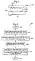
- the assembly 100 includes a substrate 102 having a plurality of conductive traces 102A, which are electrically coupled to an integrated circuit (IC), e.g., a flip chip 106, via solder bumps 104.
- a non-active side of the chip 106 includes a conductive metal.
- the conductive metal is bonded with a solder 110, e.g., an indium solder, that is located between the non-active side of the chip 106, to a heat sink 112.
- an epoxy 108 is deposited around the perimeter of the chip 106.
- the solder 110 is located to cover a surface area of approximately eighty to ninety-five percent of the chip 106 and the structural epoxy adhesive is positioned around the perimeter of the chip 106 to cover approximately five to twenty percent of the surface area of the chip 106.
- an indium solder preform and a Cookson 3090 snap cure epoxy adhesive were utilized.
- the materials were subjected to 170 degrees Celsius for two minutes to facilitate reflow of the solder and cure of the epoxy.
- the epoxy could be utilized with various other solders, such as a 10/90 Sn/Pb solder, and that a production material may broadly consist of a solder and a B-stage epoxy preform.
- thermally conductive structure for an integrated circuit has been described herein that provides a thermal joint with high thermal conductivity and longer fatigue life than current solutions.
- IC integrated circuit
- Such an epoxy-solder structure is particularly advantageous when implemented in an electronic assembly utilized in an automotive environment, as the assemblies are increasingly subjected to higher temperatures and wider temperature ranges.
- the thermally conductive structure provides for increased thermal conductivity for integrated circuit (IC) chips of electronic modules.
- the thermally conductive structure is particularly advantageous when implemented in automotive electronic modules, where higher power densities are increasingly required.
Landscapes
- Cooling Or The Like Of Semiconductors Or Solid State Devices (AREA)
Applications Claiming Priority (1)
| Application Number | Priority Date | Filing Date | Title |
|---|---|---|---|
| US11/005,277 US20060118601A1 (en) | 2004-12-06 | 2004-12-06 | Epoxy-solder thermally conductive structure for an integrated circuit |
Publications (2)
| Publication Number | Publication Date |
|---|---|
| EP1675173A2 true EP1675173A2 (fr) | 2006-06-28 |
| EP1675173A3 EP1675173A3 (fr) | 2006-07-05 |
Family
ID=36147012
Family Applications (1)
| Application Number | Title | Priority Date | Filing Date |
|---|---|---|---|
| EP05077640A Withdrawn EP1675173A3 (fr) | 2004-12-06 | 2005-11-22 | Structure thermoconductrice de soudure et époxyde pour un circuit intégré |
Country Status (2)
| Country | Link |
|---|---|
| US (1) | US20060118601A1 (fr) |
| EP (1) | EP1675173A3 (fr) |
Cited By (1)
| Publication number | Priority date | Publication date | Assignee | Title |
|---|---|---|---|---|
| DE102018131775A1 (de) * | 2018-12-11 | 2020-06-18 | Osram Opto Semiconductors Gmbh | Elektronisches Bauelement und Verfahren zur Herstellung eines elektronischen Bauelements |
Families Citing this family (1)
| Publication number | Priority date | Publication date | Assignee | Title |
|---|---|---|---|---|
| US11029677B2 (en) * | 2017-12-29 | 2021-06-08 | China Petroleum & Chemical Corporation | Method of assessing reliability of electronics assemblies under drilling vibration conditions |
Family Cites Families (17)
| Publication number | Priority date | Publication date | Assignee | Title |
|---|---|---|---|---|
| US3926904A (en) * | 1974-09-30 | 1975-12-16 | United Technologies Corp | Curable crack-resistant epoxy resin |
| JPS59208735A (ja) * | 1983-05-13 | 1984-11-27 | Hitachi Ltd | 半導体装置 |
| JPH01133337A (ja) * | 1987-11-18 | 1989-05-25 | Mitsubishi Electric Corp | 樹脂封止型半導体装置 |
| CA2002213C (fr) * | 1988-11-10 | 1999-03-30 | Iwona Turlik | Boitier de puce de circuits integres a haute performance et sa methode de fabrication |
| US5002818A (en) * | 1989-09-05 | 1991-03-26 | Hughes Aircraft Company | Reworkable epoxy die-attach adhesive |
| WO1991005368A1 (fr) * | 1989-10-05 | 1991-04-18 | Digital Equipment Corporation | Structure et procede de fixation de matrice |
| US5745344A (en) * | 1995-11-06 | 1998-04-28 | International Business Machines Corporation | Heat dissipation apparatus and method for attaching a heat dissipation apparatus to an electronic device |
| US6166434A (en) * | 1997-09-23 | 2000-12-26 | Lsi Logic Corporation | Die clip assembly for semiconductor package |
| US6144104A (en) * | 1999-03-24 | 2000-11-07 | Visteon Corporation | High-operating-temperature electronic component |
| US6307749B1 (en) * | 2000-10-23 | 2001-10-23 | Delphi Technologies, Inc. | Overmolded electronic module with underfilled surface-mount components |
| US6590292B1 (en) * | 2001-06-01 | 2003-07-08 | Lsi Logic Corporation | Thermal and mechanical attachment of a heatspreader to a flip-chip integrated circuit structure using underfill |
| JP2003292908A (ja) * | 2002-04-02 | 2003-10-15 | Three M Innovative Properties Co | 導電性及び熱伝導性を有する熱硬化型接着シート |
| US6873043B2 (en) * | 2003-03-10 | 2005-03-29 | Delphi Technologies, Inc. | Electronic assembly having electrically-isolated heat-conductive structure |
| US6943058B2 (en) * | 2003-03-18 | 2005-09-13 | Delphi Technologies, Inc. | No-flow underfill process and material therefor |
| US6700195B1 (en) * | 2003-03-26 | 2004-03-02 | Delphi Technologies, Inc. | Electronic assembly for removing heat from a flip chip |
| US7132746B2 (en) * | 2003-08-18 | 2006-11-07 | Delphi Technologies, Inc. | Electronic assembly with solder-bonded heat sink |
| US7288839B2 (en) * | 2004-02-27 | 2007-10-30 | International Business Machines Corporation | Apparatus and methods for cooling semiconductor integrated circuit package structures |
-
2004
- 2004-12-06 US US11/005,277 patent/US20060118601A1/en not_active Abandoned
-
2005
- 2005-11-22 EP EP05077640A patent/EP1675173A3/fr not_active Withdrawn
Cited By (1)
| Publication number | Priority date | Publication date | Assignee | Title |
|---|---|---|---|---|
| DE102018131775A1 (de) * | 2018-12-11 | 2020-06-18 | Osram Opto Semiconductors Gmbh | Elektronisches Bauelement und Verfahren zur Herstellung eines elektronischen Bauelements |
Also Published As
| Publication number | Publication date |
|---|---|
| US20060118601A1 (en) | 2006-06-08 |
| EP1675173A3 (fr) | 2006-07-05 |
Similar Documents
| Publication | Publication Date | Title |
|---|---|---|
| Licari et al. | Adhesives technology for electronic applications: materials, processing, reliability | |
| EP0747952B1 (fr) | Boítier à réseau de billes thermiquement amélioré | |
| EP2779231B1 (fr) | Structure de recouvrement de puissance et son procédé de fabrication | |
| US7132746B2 (en) | Electronic assembly with solder-bonded heat sink | |
| JP3677470B2 (ja) | 熱伝導構造を製造する方法 | |
| EP2916354A2 (fr) | Emballage de dispositif de semi-conducteurs intégrés ultra fin et son procédé de fabrication | |
| US20120098118A1 (en) | Compliant heat spreader for flip chip packaging | |
| US11830784B2 (en) | Leadframe spacer for double-sided power module | |
| KR100442695B1 (ko) | 열 방출판이 부착된 플립칩 패키지 제조 방법 | |
| WO1997020347A1 (fr) | Dispositif a semi-conducteur, procede de production de ce dispositif, et substrat encapsule | |
| US20060220225A1 (en) | Semiconductor packages and methods of manufacturing thereof | |
| EP1930944A2 (fr) | Interface mécanique thermique appliquée à la tranche | |
| CN1452245A (zh) | 半导体器件及其制造方法 | |
| US6888238B1 (en) | Low warpage flip chip package solution-channel heat spreader | |
| US11910518B2 (en) | Method and apparatus for heat sink mounting | |
| EP2388810A2 (fr) | Dispositif semi-conducteur avec une partie de connexion comprenant au moins deux couches de nanoparticules métalliques jointes par diffusion et procédé de fabrication correspondant | |
| US20060043603A1 (en) | Low temperature PB-free processing for semiconductor devices | |
| EP1732130A2 (fr) | Assemblage de circuits avec empaquetage IC à montage en surface et dissipateur chaleur | |
| US20070018310A1 (en) | Semiconductor device and manufacturing method thereof | |
| US7498198B2 (en) | Structure and method for stress reduction in flip chip microelectronic packages using underfill materials with spatially varying properties | |
| US7151308B2 (en) | Semiconductor chip package | |
| US20050287699A1 (en) | Electrical package employing segmented connector and solder joint | |
| US20060273467A1 (en) | Flip chip package and method of conducting heat therefrom | |
| EP1675173A2 (fr) | Structure thermoconductrice de soudure et époxyde pour un circuit intégré | |
| US20030202332A1 (en) | Second level packaging interconnection method with improved thermal and reliability performance |
Legal Events
| Date | Code | Title | Description |
|---|---|---|---|
| PUAI | Public reference made under article 153(3) epc to a published international application that has entered the european phase |
Free format text: ORIGINAL CODE: 0009012 |
|
| PUAL | Search report despatched |
Free format text: ORIGINAL CODE: 0009013 |
|
| AK | Designated contracting states |
Kind code of ref document: A2 Designated state(s): AT BE BG CH CY CZ DE DK EE ES FI FR GB GR HU IE IS IT LI LT LU LV MC NL PL PT RO SE SI SK TR |
|
| AX | Request for extension of the european patent |
Extension state: AL BA HR MK YU |
|
| AK | Designated contracting states |
Kind code of ref document: A3 Designated state(s): AT BE BG CH CY CZ DE DK EE ES FI FR GB GR HU IE IS IT LI LT LU LV MC NL PL PT RO SE SI SK TR |
|
| AX | Request for extension of the european patent |
Extension state: AL BA HR MK YU |
|
| AKX | Designation fees paid | ||
| REG | Reference to a national code |
Ref country code: DE Ref legal event code: 8566 |
|
| STAA | Information on the status of an ep patent application or granted ep patent |
Free format text: STATUS: THE APPLICATION IS DEEMED TO BE WITHDRAWN |
|
| 18D | Application deemed to be withdrawn |
Effective date: 20070106 |