EP1675175A2 - Panneau à circuit - Google Patents
Panneau à circuit Download PDFInfo
- Publication number
- EP1675175A2 EP1675175A2 EP05026073A EP05026073A EP1675175A2 EP 1675175 A2 EP1675175 A2 EP 1675175A2 EP 05026073 A EP05026073 A EP 05026073A EP 05026073 A EP05026073 A EP 05026073A EP 1675175 A2 EP1675175 A2 EP 1675175A2
- Authority
- EP
- European Patent Office
- Prior art keywords
- portions
- heat radiating
- circuit board
- wired circuit
- layer
- Prior art date
- Legal status (The legal status is an assumption and is not a legal conclusion. Google has not performed a legal analysis and makes no representation as to the accuracy of the status listed.)
- Granted
Links
Images


Classifications
-
- H—ELECTRICITY
- H05—ELECTRIC TECHNIQUES NOT OTHERWISE PROVIDED FOR
- H05K—PRINTED CIRCUITS; CASINGS OR CONSTRUCTIONAL DETAILS OF ELECTRIC APPARATUS; MANUFACTURE OF ASSEMBLAGES OF ELECTRICAL COMPONENTS
- H05K1/00—Printed circuits
- H05K1/02—Details
- H05K1/11—Printed elements for providing electric connections to or between printed circuits
- H05K1/111—Pads for surface mounting, e.g. lay-out
-
- H—ELECTRICITY
- H05—ELECTRIC TECHNIQUES NOT OTHERWISE PROVIDED FOR
- H05K—PRINTED CIRCUITS; CASINGS OR CONSTRUCTIONAL DETAILS OF ELECTRIC APPARATUS; MANUFACTURE OF ASSEMBLAGES OF ELECTRICAL COMPONENTS
- H05K1/00—Printed circuits
- H05K1/02—Details
- H05K1/0201—Thermal arrangements, e.g. for cooling, heating or preventing overheating
- H05K1/0203—Cooling of mounted components
- H05K1/0204—Cooling of mounted components using means for thermal conduction connection in the thickness direction of the substrate
- H05K1/0206—Cooling of mounted components using means for thermal conduction connection in the thickness direction of the substrate by printed thermal vias
-
- H—ELECTRICITY
- H10—SEMICONDUCTOR DEVICES; ELECTRIC SOLID-STATE DEVICES NOT OTHERWISE PROVIDED FOR
- H10W—GENERIC PACKAGES, INTERCONNECTIONS, CONNECTORS OR OTHER CONSTRUCTIONAL DETAILS OF DEVICES COVERED BY CLASS H10
- H10W40/00—Arrangements for thermal protection or thermal control
- H10W40/10—Arrangements for heating
-
- H—ELECTRICITY
- H10—SEMICONDUCTOR DEVICES; ELECTRIC SOLID-STATE DEVICES NOT OTHERWISE PROVIDED FOR
- H10W—GENERIC PACKAGES, INTERCONNECTIONS, CONNECTORS OR OTHER CONSTRUCTIONAL DETAILS OF DEVICES COVERED BY CLASS H10
- H10W40/00—Arrangements for thermal protection or thermal control
- H10W40/20—Arrangements for cooling
- H10W40/22—Arrangements for cooling characterised by their shape, e.g. having conical or cylindrical projections
- H10W40/226—Arrangements for cooling characterised by their shape, e.g. having conical or cylindrical projections characterised by projecting parts, e.g. fins to increase surface area
- H10W40/228—Arrangements for cooling characterised by their shape, e.g. having conical or cylindrical projections characterised by projecting parts, e.g. fins to increase surface area the projecting parts being wire-shaped or pin-shaped
-
- H—ELECTRICITY
- H10—SEMICONDUCTOR DEVICES; ELECTRIC SOLID-STATE DEVICES NOT OTHERWISE PROVIDED FOR
- H10W—GENERIC PACKAGES, INTERCONNECTIONS, CONNECTORS OR OTHER CONSTRUCTIONAL DETAILS OF DEVICES COVERED BY CLASS H10
- H10W70/00—Package substrates; Interposers; Redistribution layers [RDL]
- H10W70/01—Manufacture or treatment
- H10W70/05—Manufacture or treatment of insulating or insulated package substrates, or of interposers, or of redistribution layers
-
- H—ELECTRICITY
- H10—SEMICONDUCTOR DEVICES; ELECTRIC SOLID-STATE DEVICES NOT OTHERWISE PROVIDED FOR
- H10W—GENERIC PACKAGES, INTERCONNECTIONS, CONNECTORS OR OTHER CONSTRUCTIONAL DETAILS OF DEVICES COVERED BY CLASS H10
- H10W70/00—Package substrates; Interposers; Redistribution layers [RDL]
- H10W70/60—Insulating or insulated package substrates; Interposers; Redistribution layers
- H10W70/67—Insulating or insulated package substrates; Interposers; Redistribution layers characterised by their insulating layers or insulating parts
- H10W70/68—Shapes or dispositions thereof
- H10W70/685—Shapes or dispositions thereof comprising multiple insulating layers
-
- H—ELECTRICITY
- H10—SEMICONDUCTOR DEVICES; ELECTRIC SOLID-STATE DEVICES NOT OTHERWISE PROVIDED FOR
- H10W—GENERIC PACKAGES, INTERCONNECTIONS, CONNECTORS OR OTHER CONSTRUCTIONAL DETAILS OF DEVICES COVERED BY CLASS H10
- H10W74/00—Encapsulations, e.g. protective coatings
- H10W74/01—Manufacture or treatment
- H10W74/012—Manufacture or treatment of encapsulations on active surfaces of flip-chip devices, e.g. forming underfills
-
- H—ELECTRICITY
- H10—SEMICONDUCTOR DEVICES; ELECTRIC SOLID-STATE DEVICES NOT OTHERWISE PROVIDED FOR
- H10W—GENERIC PACKAGES, INTERCONNECTIONS, CONNECTORS OR OTHER CONSTRUCTIONAL DETAILS OF DEVICES COVERED BY CLASS H10
- H10W74/00—Encapsulations, e.g. protective coatings
- H10W74/10—Encapsulations, e.g. protective coatings characterised by their shape or disposition
- H10W74/15—Encapsulations, e.g. protective coatings characterised by their shape or disposition on active surfaces of flip-chip devices, e.g. underfills
-
- H—ELECTRICITY
- H05—ELECTRIC TECHNIQUES NOT OTHERWISE PROVIDED FOR
- H05K—PRINTED CIRCUITS; CASINGS OR CONSTRUCTIONAL DETAILS OF ELECTRIC APPARATUS; MANUFACTURE OF ASSEMBLAGES OF ELECTRICAL COMPONENTS
- H05K1/00—Printed circuits
- H05K1/02—Details
- H05K1/03—Use of materials for the substrate
- H05K1/05—Insulated conductive substrates, e.g. insulated metal substrate
- H05K1/056—Insulated conductive substrates, e.g. insulated metal substrate the metal substrate being covered by an organic insulating layer
-
- H—ELECTRICITY
- H05—ELECTRIC TECHNIQUES NOT OTHERWISE PROVIDED FOR
- H05K—PRINTED CIRCUITS; CASINGS OR CONSTRUCTIONAL DETAILS OF ELECTRIC APPARATUS; MANUFACTURE OF ASSEMBLAGES OF ELECTRICAL COMPONENTS
- H05K2201/00—Indexing scheme relating to printed circuits covered by H05K1/00
- H05K2201/09—Shape and layout
- H05K2201/09209—Shape and layout details of conductors
- H05K2201/095—Conductive through-holes or vias
- H05K2201/09554—Via connected to metal substrate
-
- H—ELECTRICITY
- H05—ELECTRIC TECHNIQUES NOT OTHERWISE PROVIDED FOR
- H05K—PRINTED CIRCUITS; CASINGS OR CONSTRUCTIONAL DETAILS OF ELECTRIC APPARATUS; MANUFACTURE OF ASSEMBLAGES OF ELECTRICAL COMPONENTS
- H05K2201/00—Indexing scheme relating to printed circuits covered by H05K1/00
- H05K2201/09—Shape and layout
- H05K2201/09818—Shape or layout details not covered by a single group of H05K2201/09009 - H05K2201/09809
- H05K2201/09845—Stepped hole, via, edge, bump or conductor
-
- H—ELECTRICITY
- H05—ELECTRIC TECHNIQUES NOT OTHERWISE PROVIDED FOR
- H05K—PRINTED CIRCUITS; CASINGS OR CONSTRUCTIONAL DETAILS OF ELECTRIC APPARATUS; MANUFACTURE OF ASSEMBLAGES OF ELECTRICAL COMPONENTS
- H05K2201/00—Indexing scheme relating to printed circuits covered by H05K1/00
- H05K2201/10—Details of components or other objects attached to or integrated in a printed circuit board
- H05K2201/10613—Details of electrical connections of non-printed components, e.g. special leads
- H05K2201/10621—Components characterised by their electrical contacts
- H05K2201/10674—Flip chip
-
- H—ELECTRICITY
- H05—ELECTRIC TECHNIQUES NOT OTHERWISE PROVIDED FOR
- H05K—PRINTED CIRCUITS; CASINGS OR CONSTRUCTIONAL DETAILS OF ELECTRIC APPARATUS; MANUFACTURE OF ASSEMBLAGES OF ELECTRICAL COMPONENTS
- H05K2203/00—Indexing scheme relating to apparatus or processes for manufacturing printed circuits covered by H05K3/00
- H05K2203/07—Treatments involving liquids, e.g. plating, rinsing
- H05K2203/0703—Plating
- H05K2203/0733—Method for plating stud vias, i.e. massive vias formed by plating the bottom of a hole without plating on the walls
-
- H—ELECTRICITY
- H05—ELECTRIC TECHNIQUES NOT OTHERWISE PROVIDED FOR
- H05K—PRINTED CIRCUITS; CASINGS OR CONSTRUCTIONAL DETAILS OF ELECTRIC APPARATUS; MANUFACTURE OF ASSEMBLAGES OF ELECTRICAL COMPONENTS
- H05K3/00—Apparatus or processes for manufacturing printed circuits
- H05K3/10—Apparatus or processes for manufacturing printed circuits in which conductive material is applied to the insulating support in such a manner as to form the desired conductive pattern
- H05K3/108—Apparatus or processes for manufacturing printed circuits in which conductive material is applied to the insulating support in such a manner as to form the desired conductive pattern by semi-additive methods; masks therefor
-
- H—ELECTRICITY
- H05—ELECTRIC TECHNIQUES NOT OTHERWISE PROVIDED FOR
- H05K—PRINTED CIRCUITS; CASINGS OR CONSTRUCTIONAL DETAILS OF ELECTRIC APPARATUS; MANUFACTURE OF ASSEMBLAGES OF ELECTRICAL COMPONENTS
- H05K3/00—Apparatus or processes for manufacturing printed circuits
- H05K3/40—Forming printed elements for providing electric connections to or between printed circuits
- H05K3/42—Plated through-holes or plated via connections
- H05K3/423—Plated through-holes or plated via connections characterised by electroplating method
-
- H—ELECTRICITY
- H10—SEMICONDUCTOR DEVICES; ELECTRIC SOLID-STATE DEVICES NOT OTHERWISE PROVIDED FOR
- H10W—GENERIC PACKAGES, INTERCONNECTIONS, CONNECTORS OR OTHER CONSTRUCTIONAL DETAILS OF DEVICES COVERED BY CLASS H10
- H10W70/00—Package substrates; Interposers; Redistribution layers [RDL]
- H10W70/60—Insulating or insulated package substrates; Interposers; Redistribution layers
- H10W70/67—Insulating or insulated package substrates; Interposers; Redistribution layers characterised by their insulating layers or insulating parts
- H10W70/68—Shapes or dispositions thereof
- H10W70/682—Shapes or dispositions thereof comprising holes having chips therein
-
- H—ELECTRICITY
- H10—SEMICONDUCTOR DEVICES; ELECTRIC SOLID-STATE DEVICES NOT OTHERWISE PROVIDED FOR
- H10W—GENERIC PACKAGES, INTERCONNECTIONS, CONNECTORS OR OTHER CONSTRUCTIONAL DETAILS OF DEVICES COVERED BY CLASS H10
- H10W72/00—Interconnections or connectors in packages
- H10W72/851—Dispositions of multiple connectors or interconnections
- H10W72/853—On the same surface
- H10W72/856—Bump connectors and die-attach connectors
-
- H—ELECTRICITY
- H10—SEMICONDUCTOR DEVICES; ELECTRIC SOLID-STATE DEVICES NOT OTHERWISE PROVIDED FOR
- H10W—GENERIC PACKAGES, INTERCONNECTIONS, CONNECTORS OR OTHER CONSTRUCTIONAL DETAILS OF DEVICES COVERED BY CLASS H10
- H10W90/00—Package configurations
- H10W90/701—Package configurations characterised by the relative positions of pads or connectors relative to package parts
- H10W90/721—Package configurations characterised by the relative positions of pads or connectors relative to package parts of bump connectors
- H10W90/724—Package configurations characterised by the relative positions of pads or connectors relative to package parts of bump connectors between a chip and a stacked insulating package substrate, interposer or RDL
-
- H—ELECTRICITY
- H10—SEMICONDUCTOR DEVICES; ELECTRIC SOLID-STATE DEVICES NOT OTHERWISE PROVIDED FOR
- H10W—GENERIC PACKAGES, INTERCONNECTIONS, CONNECTORS OR OTHER CONSTRUCTIONAL DETAILS OF DEVICES COVERED BY CLASS H10
- H10W90/00—Package configurations
- H10W90/701—Package configurations characterised by the relative positions of pads or connectors relative to package parts
- H10W90/731—Package configurations characterised by the relative positions of pads or connectors relative to package parts of die-attach connectors
- H10W90/734—Package configurations characterised by the relative positions of pads or connectors relative to package parts of die-attach connectors between a chip and a stacked insulating package substrate, interposer or RDL
-
- Y—GENERAL TAGGING OF NEW TECHNOLOGICAL DEVELOPMENTS; GENERAL TAGGING OF CROSS-SECTIONAL TECHNOLOGIES SPANNING OVER SEVERAL SECTIONS OF THE IPC; TECHNICAL SUBJECTS COVERED BY FORMER USPC CROSS-REFERENCE ART COLLECTIONS [XRACs] AND DIGESTS
- Y02—TECHNOLOGIES OR APPLICATIONS FOR MITIGATION OR ADAPTATION AGAINST CLIMATE CHANGE
- Y02P—CLIMATE CHANGE MITIGATION TECHNOLOGIES IN THE PRODUCTION OR PROCESSING OF GOODS
- Y02P70/00—Climate change mitigation technologies in the production process for final industrial or consumer products
- Y02P70/50—Manufacturing or production processes characterised by the final manufactured product
Definitions
- the present invention relates to a wired circuit board and, more particularly, to a wired circuit board on which semiconductor devices are mounted by a flip chip mounting method.
- Various mounting methods for mounting semiconductor devices on a wired circuit board are known, including a wire bonding mounting method, a flip chip mounting method, and an anisotropic conductive film mounting method.
- a heat radiation pattern of copper foil wiring is arranged with a wiring pattern in an area of a thermal conductive circuit board corresponding to an active device arranging area of the IC chip, so that the heat generated is radiated from the IC chip to the thermal conductive circuit board effectively (Cf. JP Laid-open (Unexamined) Publication No. 2000-323525, for example).
- a conductor of conductive to a metal base and a conductor of non-conductive to the metal base are interconnected via a thermal conducting component having a specific thermal conductivity and thereby the heat generated by electronic components is radiated to the metal base rapidly, to produce improved heat radiation (Cf. JP Laid-open (Unexamined) Publication No. Hei 11-97818, for example).
- the present invention provides a novel wired circuit board comprising a metal supporting layer, an insulating base layer which is formed on the metal supporting layer and in which an opening portion is formed, a conductive pattern, formed on the insulating base layer, to include a terminal portion for connection with a semiconductor device, and a mounting portion for mounting the semiconductor device thereon, wherein the opening portion and the terminal portion are located in the mounting portion; a heat radiating portion which is in contact with the metal supporting layer is provided in the opening portion; and a surface of the terminal portion is located close to the metal supporting layer with respect to the surface of the heat radiating portion.
- the surface of the terminal portion is located 1-15 ⁇ m closer to the metal supporting layer than the surface of the heat radiating portion.
- the surface of the terminal portion is located close to the metal supporting layer with respect to the surface of the heat radiating portion.
- This construction can provide the result that even when bumps are provided in the terminal portion so that the semiconductor device can be mounted via the bumps, the semiconductor device mounted and the heat radiating portion can be located closer to each other by an amount corresponding to the displacement of the surface of the terminal portion toward the metal supporting layer with respect to the surface of the heat radiating portion.
- the semiconductor device can be reliably mounted on the wired circuit board by the flip chip mounting method, while also the heat generated from the semiconductor device can be transferred to the metal supporting layer effectively via the heat radiating portion. This can produce the result of providing improved heat radiating ability of the wired circuit board.
- FIG. 1 is a plan view of an embodiment of a wired circuit board of the present invention, showing a principal part of a mounting portion for a semiconductor device to be mounted on.
- FIG. 2 is a sectional view of the principal part corresponding to FIG. 1.
- FIG. 3 is a sectional view of the principal part corresponding to FIG. 2, showing the mounted state of the semiconductor device.
- the wired circuit board 1 is in the form of a flexible wired circuit board, comprising a stiffener sheet 2 serving as a metal supporting layer, an insulating base layer 3 formed on the stiffener sheet 2, a conductive pattern 4 formed on the insulating base layer 3, and an insulating cover layer 5 formed on the insulating base layer 3, to cover the conductive pattern 4.
- This wired circuit board 1 has a cover opening portion 6 which is formed in a specific portion of the insulating cover layer 5 and opened in a generally rectangular shape, as viewed from top, as shown in FIG. 1.
- the inside of this cover opening portion 6 serves as a mounting portion 7 for mounting thereon a semiconductor device S (See FIG. 3).
- the stiffener sheet 2 is disposed in a portion of the wired circuit board 1 where the mounting portion 7 is provided, to stiffen the insulating base layer 3.
- the stiffener sheet 2 has thickness of e.g. 15-150 ⁇ m, or preferably 18-30 ⁇ m.
- the insulating base layer 3 is shaped like a band plate extending longitudinally of the wired circuit board 1 and is formed to have a uniform thickness of e.g. 3-20 ⁇ m, or preferably 7-12 ⁇ m (which is equivalent to thickness of an outside thick layer portion 10 and thickness of an inside thick layer portion 11 mentioned later), except a thin layer portion 9 mentioned later.
- the insulating base layer 3 has, at the mounting portion 7, a base opening portion 8 opened in a generally rectangular shape as viewed from top. It also has the thin layer portion 9 formed to surround the base opening portion 8.
- the base opening portion 8 is formed in a center portion of the mounting portion 7 to have a shape generally similar to the shape of the mounting portion 7, extending through the insulating base layer 3 in the thickness direction.
- the thin layer portion 9 is formed in a space between a marginal portion of the cover opening portion 6 and the base opening portion 8 and is shaped like a generally rectangular frame as viewed from top to surround the base opening portion 8. To be more specific, the thin layer portion 9 is formed between inside (the outside thick layer portion 10 mentioned later) spaced apart at a predetermined distance from a marginal portion of the cover opening portion 6 and outside (the inside thick layer portion 11 mentioned later) spaced apart at a predetermined distance from a marginal portion of the base opening portion 8.
- the thin layer portion 9 has a thickness of e.g. 1-15 ⁇ m, or preferably 1-8 ⁇ m.
- the insulating base layer 3 has the mounting portion 7 in which the outside thick layer portion 10 shaped like a generally rectangular frame as viewed from top, the thin layer portion 9 located inside of the outside thick layer portion 10, the inside thick layer portion 11 shaped like a generally rectangular frame as viewed from top and located inside of the thin layer portion 9, and the base opening portion 8 located inside of the inside thick layer portion 11 are formed to be arranged in the sequence mentioned above from outside (marginal portion) toward inside (center), as shown in FIG. 1.
- the conductive pattern 4 comprises a number of wirings 12 and is formed on the insulating base layer 3 to have a corresponding pattern for its intended purpose and application.
- the conductive pattern 4 has a thickness of e.g. 3-20 ⁇ m.
- the conductive pattern 4 exposed from the cover opening portion 6 serves as terminal portions 13 to be connected with a semiconductor device S.
- the terminal portions 13 are each formed in a wiring pattern in which the wirings are extended inwardly (toward the base opening portion 8) from each side (four sides) of the marginal portion of the cover opening portion 6.
- each terminal portion 13 comprises a number of wirings 12 arranged in parallel at spaced intervals in each of four areas extending from the respective sides (four sides) of the cover opening portion 6 toward the inside.
- a width W1 of each wiring 12 is set to be 10-300 ⁇ m, and a distance W2 between adjacent wirings 12 is set to be 10-300 ⁇ m.
- free ends of the wirings 12 are located on the thin layer portion 9 and are formed in the form of a circular land to be connected with the semiconductor device S.
- Each of the wirings 12 in each of the terminal portions 13 has an outside terminal portion 14 formed on the outside thick layer portion 10 and an inside terminal portion 15 formed on the thin layer portion 9, the outside terminal portion 14 and the inside terminal portion 15 being continuous with each other via a stepped portion 16 bent downwardly from the outside terminal portion 14 toward the inside terminal portion 15, as shown in FIG. 2.
- the insulating cover layer 5 is formed on the insulating base layer 3 in such a manner as to cover the conductive pattern 4 and also form the cover opening portion 6 in the mounting portion 7.
- the insulating cover layer 5 has a thickness of e.g. 3-15 ⁇ m.
- This wired circuit board 1 is provided, at the mounting portion 7, with a heat radiating portion 17 for radiating heat generated from the semiconductor device S mounted on the mounting portion 7.
- the heat radiating portion 17 has a generally rectangular shape as viewed from top and is formed on the stiffener sheet 2 in the base opening portion 8 of the mounting portion 7. A lower end portion of the heat radiating portion 17 contacts with the stiffener sheet 2, and an upper end portion of the same protrudes upwardly from the base opening portion 8 and is formed to have a generally T section so that it can be placed on a top surface of the inside thick layer portion 11.
- the heat radiating portion 17 has a thickness (a length extending between the lower surface thereof contacting with the stiffener sheet 2 and the upper surface thereof) of e.g. 6-40 ⁇ m, or preferably 10-30 ⁇ m.
- the heat radiating portion 17 is arranged in a center area defined by the wirings 12 of the terminal portions 13 extending from each side (four sides) of the marginal portion of the cover opening portion 6 inwardly (toward base opening portion 8), as shown in FIG. 1.
- the respective wirings 12 of the terminal portions 13 are arranged to surround the heat radiating portion 17.
- the surface of the heat radiating portion 17 and the surface of the outside terminal portion 14 are located higher in level than the surface of the inside terminal portion 15 (on the side thereof close to the insulating cover layer 5), as shown in FIG. 2.
- the surface of the inside terminal portion 15 is located lower in level than the surface of the surface of the outside terminal portion 14 and the surface of the heat radiating portion 17 (on the side thereof close to the stiffener sheet 2).
- a vertical interval G between the surfaces of the heat radiating portion 17 and outside terminal portion 14 and the surface of the inside terminal portion 15 is set to be e.g. 1-15 ⁇ m.
- the surface of the heat radiating portion 17 and the surface of the outside terminal portion 14 are formed to be substantially equal in level to each other.
- plating layers 18 of nickel, gold, and the like are formed on surfaces of the wirings 12 of the terminal portions 13 and the surface of the heat radiating portion 17, respectively.
- the plating layers 18 are formed by a nickel plating layer of 1-5 ⁇ m thick, a gold plating layer of 0.05-5 ⁇ m thick, and the like.
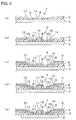
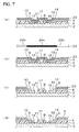
- FIGS. 4-7 show sectional views corresponding to the sectional view of FIG. 2.
- the insulating base layer 3 is formed on the stiffener sheet 2 to have a predetermined pattern, as shown in FIG. 4(a).
- a metal foil or a thin metal sheet is used as the stiffener sheet 2.
- stainless steel, 42-alloy, aluminum, copper-beryllium, phosphor bronze, and the like are used as the metal for forming the stiffer sheet.
- a stainless foil is used in terms of rigidity, corrosion resistance, and workability.
- the insulating material used for forming the insulating base layer 3 No particular limitation is imposed on the insulating material used for forming the insulating base layer 3.
- synthetic resins such as polyimide resin, polyamide imide resin, acrylic resin, polyether nitrile resin, polyether sulfonic resin, polyethylene terephthalate resin, polyethylene naphthalate resin, and polyvinyl chloride resin, are used as the insulating material used for forming the insulating base layer 3.
- polyimide resin is preferably used in terms of heat resistance and chemical resistance.
- a photosensitive synthetic resin is also preferably used in terms of easiness in microfabrication of the wiring pattern.
- a photosensitive polyimide resin is further preferably used.
- the stiffener sheet 2 is prepared, first, as shown in FIG. 5(a). Then, a varnish of precursor of the photosensitive polyimide resin (photosensitive polyamic acid resin) is coated over the entire surface of the stiffener sheet 2, as shown in FIG. 5(b). Then, the coated varnish is heated at e.g. 60-150°C, or preferably at 80-120°C, to form a coating 19 of the precursor of the photosensitive polyimide resin.
- precursor of the photosensitive polyimide resin photosensitive polyamic acid resin
- the photo mask 20 has a predetermined pattern comprising light shielding portions 20a, semi-light-transmitting portions 20b and total-light-transmitting portions 20c.
- the semi-light-transmitting portions 20b permit light to transmit in a light transmission ratio properly selected from the range falling within 1-99%.
- the photo mask 20 is disposed opposite the coating 19 so that the light shielding portions 20a confront portions of the coating 19 where the base opening portions 8 are to be formed in the insulating base layer 3 on the stiffener sheet 2; the semi-light-transmitting portions 20b confront portions of the coating 19 where the thin layer portions 9 of the insulating base layer 3 are to be formed on the stiffener sheet 2; and the total-light-transmitting portions 20c confront portions of the insulating base layer 3 (including the outside thick layer portions 10 and the inside thick layer portions 11) other than the thin layer portions 9 are to be formed on the stiffener sheet 2.
- Radiation irradiated through the photo mask 20 has an exposure wavelength of 300-450nm, and an integrated quantity of exposure light is in the range of 100-2,000mJ/cm 2 .
- the coating 19 thus exposed is heated to a predetermined temperature, if necessary, it is developed, as shown in FIG. 5(d).
- the exposed-to-light portion of the coating 19 irradiated is heated at a temperature in the range of e.g. 130°C or more to less than 150°C, it is solubilized (positive pattern) in the next developing process.
- it is insolubilized (negative pattern) in the next developing process.
- the development can be performed by any known method, such as a dipping process and a spraying process, using a known developing solution such as, for example, an alkaline developer.
- a known developing solution such as, for example, an alkaline developer.
- the coating 19 is formed in a predetermined pattern in which the portions thereof (including the outside thick layer portions 10 and the inside thick layer portions 11), which confronted the total-light-transmitting portions 20c of the photo mask 20, remain; the portions thereof for the base opening portions 8 to be formed, which confronted the light shielding portions 20a of the photo mask 20, melt; and the portions thereof for the thin layer portions 9 to be formed, which confronted the semi-light-transmitting portions 20b of the photo mask 20, melt at a residual ratio corresponding to the light transmittance.
- the coating 19 formed in a predetermined pattern is heated finally to e.g. 250°C or more to be cured (imidized).
- the insulating base layer 3 of polyimide resin is formed in the predetermined pattern having the outside thick layer portions 10, the thin layer portions 9, the inside thick layer portions 11, and the base opening portions 8 formed at the corresponding portion thereof to the mounting portion 7, as shown in FIG. 5(e).
- a dry film is bonded onto the stiffener sheet 2 by fusion bonding, or by adhesive bonding using an adhesive layer, if necessary, first. Then the dry film thus bonded is formed in a predetermined pattern having the outside thick layer portions 10, the thin layer portions 9, the inside thick layer portions 11, and the base opening portions 8 formed at the corresponding portions thereof to the mounting portions 7 by dry etching using plasma or laser, or by wet etching using an alkaline solution.
- the conductor layer 4 and the heat radiating portion 17 are formed simultaneously, as shown in FIG. 4(b).
- the conductive materials that may be used include, for example, copper, nickel, gold, solder, or alloys thereof. Copper is preferably used in terms of electrical conductivity, availability at low cost, and workability.
- the conductive pattern 4 and the heat radiating portion 17 are formed by a known patterning process, such as a subtractive process and an additive process.
- a subtractive process such as a subtractive process
- an additive process is preferably used.
- a thin metal film 21 of a seed film is formed on the entire surface of the insulating base layer 3, first, as shown in FIG. 6(a). Chromium, nickel, copper, and alloys thereof are preferably used as the metal material used for forming the thin metal film 21. Though no particular limitation is imposed on the formation of the thin metal film 21, the thin metal film 21 is formed using e.g. a vacuum deposition process such as a sputtering process. The thin metal film 21 has thickness of e.g. 100-3,000 ⁇ .
- the thin metal film 21 may be formed in multilayer by for example forming a thin chromium film and a thin copper film sequentially by the sputtering process.
- a plating resist 22 having a reverse pattern to the conductive pattern 4 and the heat radiating portion 17 is formed on a surface of the thin metal film 21, as shown in FIG. 6(b).
- the plating resist 22 may be formed in the form of the reverse pattern mentioned above to the conductive pattern 4 and the heat radiating portion 17 by a known process using a dry film photoresist, for example.
- the conductive pattern 4 and the heat radiating portion 17 are formed simultaneously on a surface of the thin metal film 21 exposed from the plating resist 22, as shown in FIG. 6(c).
- electrolytic plating or preferably electrolytic copper plating, is used for forming the conductive pattern 4 and the heat radiating portion 17.
- the plating resist 22 is removed, as shown in FIG. 6(d).
- the plating resist 22 is removed by a known etching process, such as, for example, chemical etching (wet etching), or by stripping.
- the thin metal film 21 exposed from the conductive pattern 4 and the heat radiating portion 17 is removed, as shown in FIG. 6(e).
- the thin metal film 21 is removed by chemical etching (wet etching), for example.
- the conductive pattern 4 including the terminal portions 13 mentioned above and the heat radiating portion 17 are formed.
- the thin metal film 21 shown in FIG. 6 is omitted.
- the insulating cover layer 5 of a predetermined pattern is formed on the insulating base layer 3, to cover the conductive pattern 4, except the terminal portions 13, as shown in FIG. 4(c).
- the same insulating material as that for the insulating base layer 3 is used for forming the insulating cover layer 5.
- photosensitive polyimide resin is used.
- a solution of precursor of the photosensitive polyimide resin (photosensitive polyamic acid resin) is coated over the entire surface of the insulating base layer 3 including the conductive pattern 4, as shown in FIG. 7(a), and then is heated at e.g. 60-150°C, or preferably at 80-120°C, to form a coating 23 of the precursor of the photosensitive polyimide resin.
- the photo mask 24 has a predetermined pattern comprising light shielding portions 24a and total-light-transmitting portions 24b.
- the photo mask 24 is disposed opposite the coating 23 so that the light shielding portions 24a confront the cover opening portions 6 of the insulating cover layer 5 and the total-light-transmitting portions 24b confront the remaining portions of the insulating cover layer 5.
- the coating 23 is exposed to light in the same manner as the coating 19 mentioned above.
- the coating 23 thus exposed is developed in the same manner as the coating 19, as shown in FIG. 7(c).
- the coating 23 is formed in the negative pattern.
- the coating 23 is formed in a predetermined pattern in which the portions thereof corresponding to the cover opening portions 6, which confronted the light shielding portions 24a of the photo mask 24, melt and the mounting portions 7 are exposed.
- the coating 23 formed in a predetermined pattern is heated finally to e.g. 250°C or more to be cured (imidized).
- the insulating cover layer 5 of polyimide resin is formed in the predetermined pattern in which the mounting portions 7 are exposed from the cover opening portions 6 and the conductive patterns 4 are covered, except the terminal portions 13 disposed on the mounting portions 7, as shown in FIG. 7(d).
- the photosensitive synthetic resin for example a dry film is bonded onto the insulating base layer 3 by fusion bonding, or by adhesive bonding using an adhesive layer, if necessary, first. Then the dry film thus bonded is formed in a predetermined pattern in which the mounting portions 7 are exposed from the cover opening portions 6 by dry etching using plasma or laser, or by wet etching using an alkaline solution and the conductive patterns 4 are covered, except the terminal portions 13 disposed on the mounting portions 7.
- the plating layers 18 are formed on the terminal portions 13 and the heat radiating portion 17, to protect surfaces of the terminal portions 13, as shown in FIG. 4(d).
- the plating material for forming the plating layers 18. nickel and gold are used for forming the plating layers 18.
- the plating layers 18 are formed by the electrolytic plating or the electroless plating, with the portions of the mounting portions 7, except the surfaces of the terminal portions 13 and the heat radiating portion 17, covered with the plating resist.
- the plating layer 18 may be formed in multilayer by, for example, plating the terminal portions 13 with nickel and gold sequentially.
- the stiffener sheet 2 is etched to leave its portions corresponding to the mounting portions 17 of the wired circuit board 1, as shown in FIG. 4(e).
- the stiffener sheet 2 is subjected to the wet-etching using ferric chloride solution.
- the surface of the inside terminal portion 15 surrounding the heat radiating portion 17 in the mounting portion 7 is located lower in level than the surface of the heat radiating portion 17, as mentioned above.
- This construction can provide the result that even when bumps 25 of gold or solder are provided on the surface of the inside terminal portion 15 so that the semiconductor device S can be mounted via the bumps 25, the semiconductor device S mounted and the heat radiating portion 17 can be located closer to each other by an amount corresponding to the downward displacement of the surface of the inside terminal portion 15 with respect to the surface of the heat radiating portion 17.
- the semiconductor device S can be reliably mounted on the wired circuit board 1 by the flip chip mounting method, while also the heat generated from the semiconductor device S can be transferred to the stiffener sheet 2 effectively via the heat radiating portion 17. This can produce the result of providing improved heat radiating ability of the wired circuit board 1.
- the stiffer sheet 2 of stainless steel (SUS304) having thickness of 20 ⁇ m was prepared (Cf. FIG. 5(a)).
- a solution of precursor of a photosensitive polyimide resin (photosensitive polyamic acid resin) was coated over the entire surface of the stiffener sheet 2. Then, the coated solution was heated for 2 minutes at 120°C, to form the coating 19 of the precursor of the photosensitive polyimide resin (Cf. FIG. 5(b)).
- the photo mask 20 was disposed opposite the coating 19 so that the light shielding portions 20a confronted portions of the coating 19 where the base opening portions 8 were to be formed in the insulating base layer 3 on the stiffener sheet 2; the semi-light-transmitting portions 20b confronted portions of the coating 19 where the thin layer portions 9 of the insulating base layer 3 were to be formed on the stiffener sheet 2; and the total-light-transmitting portions 20c confronted portions of the insulating base layer 3 except the thin layer portions 9 were to be formed on the stiffener sheet 2. Then, the coating 19 was exposed to light with ultraviolet (an integrated quantity of exposure light of 720mJ/cm 2 (Cf. FIG. 5(c)).
- the coating 19 thus exposed was heated (for three minutes at 160°C), it was developed using the alkaline developer, to form the coating 19 in a predetermined pattern comprising the base opening portions 8 and the thin layer portions 9 (Cf. FIG. 5(d)). Thereafter, the coating 19 was heated at 420°C to thereby produce the insulating base layer 3 of polyimide resin having thickness of 10 ⁇ m (whose thin layer portion 9 has thickness of 5 ⁇ m (Cf. FIG. 5(e)).
- the base opening portion 8 was formed in a square, 2 ⁇ m on a side, as viewed from top.
- the thin chromium film and the thin copper film were sequentially formed on the entire surface of the insulating base layer 3 by the sputtering process, to form the thin metal film 21 having thickness of 2,000 ⁇ (Cf. FIG 6(a)). Then, after the dry film resist was laminated on the surface of the thin metal film 21, the thin metal film 21 was exposed to light with ultraviolet (an integrated quantity of exposure light of 235mJ/cm 2 ) and then developed by the alkaline developer, to form the plating resist 22 of a reverse pattern to the conductive pattern 4 and the heat radiating portion 17 (Cf. FIG. 6(b)).
- ultraviolet an integrated quantity of exposure light of 235mJ/cm 2
- the conductive pattern 4 having thickness of 10 ⁇ m and the heat radiating portion 17 were formed on the surface of the thin metal film 21 exposed from the plating resist 22 (Cf. FIG. 6(c)) and, thereafter, the plating resist 22 was stripped (Cf. FIG. 6(d)). Then, the thin metal film 21 exposed from the conductive pattern 4 and the heat radiating portion 17 was removed by the chemical etching (Cf. FIG. 6(e)).
- the solution of precursor of the photosensitive polyimide resin was coated over the entire surface of the conductive pattern 4 and insulating base layer 3 and then was heated for two minutes at 120°C, to form the coating 23 of the precursor of the photosensitive polyimide resin (Cf. FIG. 7(a)).
- the photo mask 24 was disposed opposite the coating 23 so that the light shielding portions 24a confronted the cover opening portions 6 of the insulating cover layer 5 and the total-light-transmitting portions 24b confronted the remaining portions of the insulating cover layer 5. Then, the coating 23 was exposed with ultraviolet (an integrated quantity of exposure light of 720mJ/cm 2 ) (Cf. FIG. 7(b)).
- the coating 23 thus exposed was subjected to the heating (for three minutes at 160°C) after the exposure to light, it was developed by the alkaline developer, whereby the coating 23 was formed in a predetermined pattern in which the mounting portions 7 were exposed from the cover opening portions 6 and all portions of the conductive pattern 4, except the terminals 13 disposed in the mounting portions 7, were covered (Cf. FIG. 7(c)). Thereafter, the coating 23 wad heated at 420°C to thereby form the insulating cover layer 5 of polyimide resin having thickness of 3 ⁇ m (Cf. FIG. 7(d)).
- the plating layers 18 of 0.1 ⁇ m thick were formed on the terminal portions 13 by the electroless gold plating (Cf. FIG. 4(d)).
- the stiffener sheet 2 was etched by wet etching using ferric chloride solution, to leave its portions corresponding to the mounting portions 17 of the wired circuit board 1 (Cf. FIG. 4(e)), thereby producing the wired circuit board 1.
- the surface of the inside terminal portion 15 was located 5 ⁇ m lower in level than the surface of the heat radiating portion 17.
- Example 1 Except that the insulating base layer 3 having uniform thickness was formed without forming the thin layer portion 9 in the formation of the insulating base layer 3, the same method as in Example 1 was used to form the wired circuit board.
- the surface of the inside terminal portion 15 was located on the same level with the surface of the heat radiating portion 17.
- the semiconductor devices were mounted on the mounting portions of the wired circuit board of Example 1 and the wired circuit board of Comparative Example 1, respectively, via gold bumps by the flip chip mounting method. Thereafter, the semiconductor devices were energized.
- the wired circuit board of Example 1 exhibited the good heat radiating ability so that the semiconductor device was operated in good condition, while on the other hand, the wired circuit board of Comparative Example exhibits the poor heat radiating ability so that the semiconductor device was sometimes operated in poor condition.
Landscapes
- Engineering & Computer Science (AREA)
- Microelectronics & Electronic Packaging (AREA)
- Structure Of Printed Boards (AREA)
- Cooling Or The Like Of Semiconductors Or Solid State Devices (AREA)
- Structures For Mounting Electric Components On Printed Circuit Boards (AREA)
- Wire Bonding (AREA)
Applications Claiming Priority (1)
| Application Number | Priority Date | Filing Date | Title |
|---|---|---|---|
| JP2004369871A JP2006179606A (ja) | 2004-12-21 | 2004-12-21 | 配線回路基板 |
Publications (3)
| Publication Number | Publication Date |
|---|---|
| EP1675175A2 true EP1675175A2 (fr) | 2006-06-28 |
| EP1675175A3 EP1675175A3 (fr) | 2008-09-10 |
| EP1675175B1 EP1675175B1 (fr) | 2010-05-19 |
Family
ID=36129779
Family Applications (1)
| Application Number | Title | Priority Date | Filing Date |
|---|---|---|---|
| EP05026073A Ceased EP1675175B1 (fr) | 2004-12-21 | 2005-11-30 | Panneau à circuit |
Country Status (5)
| Country | Link |
|---|---|
| US (1) | US7271347B2 (fr) |
| EP (1) | EP1675175B1 (fr) |
| JP (1) | JP2006179606A (fr) |
| CN (1) | CN1805657B (fr) |
| DE (1) | DE602005021305D1 (fr) |
Cited By (1)
| Publication number | Priority date | Publication date | Assignee | Title |
|---|---|---|---|---|
| EP2091309A3 (fr) * | 2008-02-12 | 2009-10-14 | Nitto Denko Corporation | Procédé de fabrication d'une carte à circuit imprimé |
Families Citing this family (22)
| Publication number | Priority date | Publication date | Assignee | Title |
|---|---|---|---|---|
| US7982307B2 (en) * | 2006-11-22 | 2011-07-19 | Agere Systems Inc. | Integrated circuit chip assembly having array of thermally conductive features arranged in aperture of circuit substrate |
| US8233287B2 (en) | 2007-02-07 | 2012-07-31 | Nitto Denko Corporation | Ground vias for enhanced preamp heat release in hard disk drives |
| JP5025399B2 (ja) * | 2007-09-27 | 2012-09-12 | 新光電気工業株式会社 | 配線基板及びその製造方法 |
| JP2009129490A (ja) * | 2007-11-21 | 2009-06-11 | Nitto Denko Corp | 配線回路基板 |
| DE102008052244A1 (de) * | 2008-10-18 | 2010-04-22 | Carl Freudenberg Kg | Flexible Leiterplatte |
| JP2010166025A (ja) * | 2008-12-19 | 2010-07-29 | Panasonic Corp | 実装構造 |
| TWI377653B (en) * | 2009-02-16 | 2012-11-21 | Unimicron Technology Corp | Package substrate strucutre with cavity and method for making the same |
| US8222748B2 (en) * | 2009-05-29 | 2012-07-17 | Texas Instruments Incorporated | Packaged electronic devices having die attach regions with selective thin dielectric layer |
| JP5418308B2 (ja) * | 2010-03-08 | 2014-02-19 | 日本電気株式会社 | 実装構造 |
| JP5711472B2 (ja) * | 2010-06-09 | 2015-04-30 | 新光電気工業株式会社 | 配線基板及びその製造方法並びに半導体装置 |
| KR101184006B1 (ko) * | 2010-09-28 | 2012-09-19 | 삼성전기주식회사 | 인쇄회로기판 및 그 제조방법 |
| JP2013026367A (ja) * | 2011-07-20 | 2013-02-04 | Teramikros Inc | 半導体装置及びその製造方法 |
| JP2013149947A (ja) * | 2011-12-19 | 2013-08-01 | Shinko Electric Ind Co Ltd | 発光素子搭載用パッケージ及び発光素子パッケージ並びにそれらの製造方法 |
| JP2013207093A (ja) * | 2012-03-28 | 2013-10-07 | Nippon Mektron Ltd | フレキシブルプリント配線板およびその製造方法 |
| GB2520952A (en) | 2013-12-04 | 2015-06-10 | Ibm | Flip-chip electronic device with carrier having heat dissipation elements free of solder mask |
| KR102347394B1 (ko) * | 2015-02-12 | 2022-01-06 | 삼성전자주식회사 | 회로 기판을 포함하는 전자 장치 |
| CN104810322A (zh) * | 2015-05-18 | 2015-07-29 | 京东方科技集团股份有限公司 | 阵列基板及其制造方法、显示面板、显示装置、掩模板 |
| JP6652443B2 (ja) * | 2016-05-06 | 2020-02-26 | 株式会社日本マイクロニクス | 多層配線基板及びこれを用いたプローブカード |
| JP6965315B2 (ja) * | 2019-08-21 | 2021-11-10 | 日東電工株式会社 | 配線回路基板、容器および基板収容セット |
| KR102911692B1 (ko) * | 2022-03-04 | 2026-01-13 | 동우 화인켐 주식회사 | 방열판 및 이의 제조방법 |
| KR102553123B1 (ko) * | 2022-09-08 | 2023-07-11 | 주식회사 에이플렉스 | 칩의 손상이 방지된 연성인쇄회로기판 |
| TWI873949B (zh) * | 2022-11-11 | 2025-02-21 | 財團法人工業技術研究院 | 模塑電子組件 |
Citations (1)
| Publication number | Priority date | Publication date | Assignee | Title |
|---|---|---|---|---|
| US5920458A (en) | 1997-05-28 | 1999-07-06 | Lucent Technologies Inc. | Enhanced cooling of a heat dissipating circuit element |
Family Cites Families (11)
| Publication number | Priority date | Publication date | Assignee | Title |
|---|---|---|---|---|
| US5050040A (en) * | 1988-10-21 | 1991-09-17 | Texas Instruments Incorporated | Composite material, a heat-dissipating member using the material in a circuit system, the circuit system |
| US5172301A (en) * | 1991-10-08 | 1992-12-15 | Lsi Logic Corporation | Heatsink for board-mounted semiconductor devices and semiconductor device assembly employing same |
| ES2130961B1 (es) * | 1996-09-27 | 2000-03-01 | Batz S Coop Ltda | Gato para vehiculos. |
| US5856911A (en) * | 1996-11-12 | 1999-01-05 | National Semiconductor Corporation | Attachment assembly for integrated circuits |
| JPH1197818A (ja) | 1997-09-16 | 1999-04-09 | Toyota Autom Loom Works Ltd | 実装配線基板 |
| JPH11248032A (ja) | 1998-02-27 | 1999-09-14 | Tokyo Kousou Kk | 高圧力減圧調節弁 |
| JP2000012723A (ja) * | 1998-06-23 | 2000-01-14 | Nitto Denko Corp | 回路基板の実装構造体およびそれに用いる多層回路基板 |
| JP3160583B2 (ja) * | 1999-01-27 | 2001-04-25 | 日本特殊陶業株式会社 | 樹脂製基板 |
| JP3196762B2 (ja) * | 1999-04-20 | 2001-08-06 | 日本電気株式会社 | 半導体チップ冷却構造 |
| JP3446818B2 (ja) | 1999-05-10 | 2003-09-16 | 日本電気株式会社 | 半導体装置の実装構造、及びその製造方法 |
| US6744135B2 (en) * | 2001-05-22 | 2004-06-01 | Hitachi, Ltd. | Electronic apparatus |
-
2004
- 2004-12-21 JP JP2004369871A patent/JP2006179606A/ja active Pending
-
2005
- 2005-11-30 EP EP05026073A patent/EP1675175B1/fr not_active Ceased
- 2005-11-30 DE DE602005021305T patent/DE602005021305D1/de not_active Expired - Lifetime
- 2005-12-19 US US11/305,120 patent/US7271347B2/en not_active Expired - Lifetime
- 2005-12-21 CN CN2005101370793A patent/CN1805657B/zh not_active Expired - Fee Related
Patent Citations (1)
| Publication number | Priority date | Publication date | Assignee | Title |
|---|---|---|---|---|
| US5920458A (en) | 1997-05-28 | 1999-07-06 | Lucent Technologies Inc. | Enhanced cooling of a heat dissipating circuit element |
Cited By (2)
| Publication number | Priority date | Publication date | Assignee | Title |
|---|---|---|---|---|
| EP2091309A3 (fr) * | 2008-02-12 | 2009-10-14 | Nitto Denko Corporation | Procédé de fabrication d'une carte à circuit imprimé |
| US8198017B2 (en) | 2008-02-12 | 2012-06-12 | Nitto Denko Corporation | Producing method of wired circuit board |
Also Published As
| Publication number | Publication date |
|---|---|
| CN1805657A (zh) | 2006-07-19 |
| US20060131065A1 (en) | 2006-06-22 |
| EP1675175A3 (fr) | 2008-09-10 |
| US7271347B2 (en) | 2007-09-18 |
| EP1675175B1 (fr) | 2010-05-19 |
| DE602005021305D1 (de) | 2010-07-01 |
| JP2006179606A (ja) | 2006-07-06 |
| CN1805657B (zh) | 2010-05-12 |
Similar Documents
| Publication | Publication Date | Title |
|---|---|---|
| EP1675175B1 (fr) | Panneau à circuit | |
| US8030576B2 (en) | Wired circuit board with interposed metal thin film and producing method thereof | |
| US7659605B2 (en) | COF board | |
| US7569773B2 (en) | Wired circuit board | |
| JP2014160857A (ja) | フリップ・チップ・オン・フレックス(flip−chip−on−flex)の応用例用のフレキシブル回路基板 | |
| US7405479B2 (en) | Wired circuit board | |
| CN100586251C (zh) | 布线电路板 | |
| EP1651016B1 (fr) | Circuit imprimé muni de pastilles destinées à être connectées à des pastilles externes à l'aide de métal fondu | |
| CN100392517C (zh) | 带有电路的悬挂基板 | |
| KR20100025572A (ko) | 금속 코어 기재를 포함하는 회로 어셈블리 및 그의 제조 방법 | |
| US6977349B2 (en) | Method for manufacturing wiring circuit boards with bumps and method for forming bumps | |
| CN109429442B (zh) | 电路板及其制作方法 | |
| US20070023877A1 (en) | Chip on flex tape with dimension retention pattern | |
| CN100505990C (zh) | 双面印刷电路板的制造方法 | |
| CN1979673B (zh) | 配线电路基板及其制造方法 | |
| EP1173051B1 (fr) | Carte de circuits imprimes flexible et son procede de production | |
| JP2000091048A (ja) | 導通補助材及びその製造方法 | |
| WO2005027221A1 (fr) | Ruban de puces sur flexible | |
| JP2004072027A (ja) | 突起電極付き配線基板の製造方法 | |
| CN119893858A (zh) | 电路板的制作方法、电路板以及电路板组件 | |
| JPH06188534A (ja) | 電子部品搭載用基板及びその製造方法 | |
| JP2006013160A (ja) | 配線回路基板および半導体装置 | |
| JP2006049587A (ja) | プリント配線板及びその製造方法 | |
| TW557645B (en) | Flexible printed wiring board and its production method | |
| JPH0260233B2 (fr) |
Legal Events
| Date | Code | Title | Description |
|---|---|---|---|
| PUAI | Public reference made under article 153(3) epc to a published international application that has entered the european phase |
Free format text: ORIGINAL CODE: 0009012 |
|
| AK | Designated contracting states |
Kind code of ref document: A2 Designated state(s): AT BE BG CH CY CZ DE DK EE ES FI FR GB GR HU IE IS IT LI LT LU LV MC NL PL PT RO SE SI SK TR |
|
| AX | Request for extension of the european patent |
Extension state: AL BA HR MK YU |
|
| PUAL | Search report despatched |
Free format text: ORIGINAL CODE: 0009013 |
|
| AK | Designated contracting states |
Kind code of ref document: A3 Designated state(s): AT BE BG CH CY CZ DE DK EE ES FI FR GB GR HU IE IS IT LI LT LU LV MC NL PL PT RO SE SI SK TR |
|
| AX | Request for extension of the european patent |
Extension state: AL BA HR MK YU |
|
| 17P | Request for examination filed |
Effective date: 20090127 |
|
| AKX | Designation fees paid |
Designated state(s): DE FR GB |
|
| GRAP | Despatch of communication of intention to grant a patent |
Free format text: ORIGINAL CODE: EPIDOSNIGR1 |
|
| GRAS | Grant fee paid |
Free format text: ORIGINAL CODE: EPIDOSNIGR3 |
|
| GRAA | (expected) grant |
Free format text: ORIGINAL CODE: 0009210 |
|
| AK | Designated contracting states |
Kind code of ref document: B1 Designated state(s): DE FR GB |
|
| REG | Reference to a national code |
Ref country code: GB Ref legal event code: FG4D |
|
| REF | Corresponds to: |
Ref document number: 602005021305 Country of ref document: DE Date of ref document: 20100701 Kind code of ref document: P |
|
| PLBE | No opposition filed within time limit |
Free format text: ORIGINAL CODE: 0009261 |
|
| STAA | Information on the status of an ep patent application or granted ep patent |
Free format text: STATUS: NO OPPOSITION FILED WITHIN TIME LIMIT |
|
| 26N | No opposition filed |
Effective date: 20110222 |
|
| REG | Reference to a national code |
Ref country code: DE Ref legal event code: R097 Ref document number: 602005021305 Country of ref document: DE Effective date: 20110221 |
|
| REG | Reference to a national code |
Ref country code: FR Ref legal event code: PLFP Year of fee payment: 11 |
|
| REG | Reference to a national code |
Ref country code: FR Ref legal event code: PLFP Year of fee payment: 12 |
|
| REG | Reference to a national code |
Ref country code: FR Ref legal event code: PLFP Year of fee payment: 13 |
|
| REG | Reference to a national code |
Ref country code: FR Ref legal event code: PLFP Year of fee payment: 14 |
|
| PGFP | Annual fee paid to national office [announced via postgrant information from national office to epo] |
Ref country code: DE Payment date: 20181120 Year of fee payment: 14 |
|
| PGFP | Annual fee paid to national office [announced via postgrant information from national office to epo] |
Ref country code: GB Payment date: 20181128 Year of fee payment: 14 Ref country code: FR Payment date: 20181011 Year of fee payment: 14 |
|
| REG | Reference to a national code |
Ref country code: DE Ref legal event code: R119 Ref document number: 602005021305 Country of ref document: DE |
|
| GBPC | Gb: european patent ceased through non-payment of renewal fee |
Effective date: 20191130 |
|
| PG25 | Lapsed in a contracting state [announced via postgrant information from national office to epo] |
Ref country code: DE Free format text: LAPSE BECAUSE OF NON-PAYMENT OF DUE FEES Effective date: 20200603 Ref country code: FR Free format text: LAPSE BECAUSE OF NON-PAYMENT OF DUE FEES Effective date: 20191130 Ref country code: GB Free format text: LAPSE BECAUSE OF NON-PAYMENT OF DUE FEES Effective date: 20191130 |