EP1677093A2 - Nahfeldmessgerät für Filmdicke - Google Patents
Nahfeldmessgerät für Filmdicke Download PDFInfo
- Publication number
- EP1677093A2 EP1677093A2 EP05112757A EP05112757A EP1677093A2 EP 1677093 A2 EP1677093 A2 EP 1677093A2 EP 05112757 A EP05112757 A EP 05112757A EP 05112757 A EP05112757 A EP 05112757A EP 1677093 A2 EP1677093 A2 EP 1677093A2
- Authority
- EP
- European Patent Office
- Prior art keywords
- film
- light
- field
- thickness
- detector
- Prior art date
- Legal status (The legal status is an assumption and is not a legal conclusion. Google has not performed a legal analysis and makes no representation as to the accuracy of the status listed.)
- Granted
Links
Images


Classifications
-
- G—PHYSICS
- G01—MEASURING; TESTING
- G01Q—SCANNING-PROBE TECHNIQUES OR APPARATUS; APPLICATIONS OF SCANNING-PROBE TECHNIQUES, e.g. SCANNING PROBE MICROSCOPY [SPM]
- G01Q60/00—Particular types of SPM [Scanning Probe Microscopy] or microscopes; Essential components thereof
- G01Q60/18—SNOM [Scanning Near-Field Optical Microscopy] or apparatus therefor, e.g. SNOM probes
- G01Q60/22—Probes, their manufacture, or their related instrumentation, e.g. holders
-
- B—PERFORMING OPERATIONS; TRANSPORTING
- B82—NANOTECHNOLOGY
- B82Y—SPECIFIC USES OR APPLICATIONS OF NANOSTRUCTURES; MEASUREMENT OR ANALYSIS OF NANOSTRUCTURES; MANUFACTURE OR TREATMENT OF NANOSTRUCTURES
- B82Y20/00—Nanooptics, e.g. quantum optics or photonic crystals
-
- B—PERFORMING OPERATIONS; TRANSPORTING
- B82—NANOTECHNOLOGY
- B82Y—SPECIFIC USES OR APPLICATIONS OF NANOSTRUCTURES; MEASUREMENT OR ANALYSIS OF NANOSTRUCTURES; MANUFACTURE OR TREATMENT OF NANOSTRUCTURES
- B82Y35/00—Methods or apparatus for measurement or analysis of nanostructures
-
- G—PHYSICS
- G01—MEASURING; TESTING
- G01B—MEASURING LENGTH, THICKNESS OR SIMILAR LINEAR DIMENSIONS; MEASURING ANGLES; MEASURING AREAS; MEASURING IRREGULARITIES OF SURFACES OR CONTOURS
- G01B11/00—Measuring arrangements characterised by the use of optical techniques
- G01B11/02—Measuring arrangements characterised by the use of optical techniques for measuring length, width or thickness
- G01B11/06—Measuring arrangements characterised by the use of optical techniques for measuring length, width or thickness for measuring thickness ; e.g. of sheet material
- G01B11/0616—Measuring arrangements characterised by the use of optical techniques for measuring length, width or thickness for measuring thickness ; e.g. of sheet material of coating
- G01B11/0625—Measuring arrangements characterised by the use of optical techniques for measuring length, width or thickness for measuring thickness ; e.g. of sheet material of coating with measurement of absorption or reflection
-
- G—PHYSICS
- G01—MEASURING; TESTING
- G01Q—SCANNING-PROBE TECHNIQUES OR APPARATUS; APPLICATIONS OF SCANNING-PROBE TECHNIQUES, e.g. SCANNING PROBE MICROSCOPY [SPM]
- G01Q30/00—Auxiliary means serving to assist or improve the scanning probe techniques or apparatus, e.g. display or data processing devices
- G01Q30/02—Non-SPM analysing devices, e.g. SEM [Scanning Electron Microscope], spectrometer or optical microscope
Definitions
- the present invention relates to film-thickness measurement apparatuses, and in particular to an improvement in the spatial resolution thereof.
- film-thickness measurement apparatuses for non-contact, non-destructive measurement of the film thickness of film samples using optical interference.
- Such apparatuses use microscope spectrometers and so forth to measure the interference spectrum due to light reflected from the front surface and rear surface of the film and obtain the film thickness (for example, see Japanese Unexamined Patent Application Publication No. H05-302816 and Japanese Unexamined Patent Application Publication No. H07-4922).
- the film thickness d can be calculated from the waveform of the interference spectrum based on equation (1) below.
- N is the number of valleys (minimal points) included between the wave numbers ⁇ 1 and ⁇ 2
- n is the refractive index of the film sample
- ⁇ is the angle of incidence of the light.
- the film-thickness measurement apparatuses described above are not capable of performing measurement at a scale smaller than the wavelength of the light used for measurement, as standard optical measurement apparatuses. In other words, like other optical measurement apparatuses, the spatial resolution is limited by the diffraction limit of light. Accordingly, as disclosed in Japanese Unexamined Patent Application Publication No. 2004-264118, a film-thickness measurement apparatus using near-field optics has been proposed.
- the apparatus disclosed in Japanese Unexamined Patent Application Publication No. 2004-264118 performs measurement in a so-called illumination-collection mode using an aperture-type near-field probe. That is, near-field light is emitted from a minute aperture in the probe to illuminate the sample, and scattered light due to the interaction between the near-field light and the sample passes through the aperture again and is collected.
- the present invention has been conceived in light of the problems described above, and an object thereof is to provide a near-field film-thickness measurement apparatus having a spatial resolution at or below the wavelength of light and having sufficient film-thickness measurement precision.
- a near-field film-thickness measurement apparatus of the present invention comprises a scattering near-field probe, a light source, a detector, a spectroscope disposed in an optical path between the light source and the detector, and a film-thickness calculating unit.
- the light source emits excitation light for generating near-field light at a tip of the near-field probe and/or at a surface of a film sample.
- the detector detects, as measurement light, scattered light generated by bringing the tip of the near-field probe and the surface of the film sample close to the region of the near-field light.
- the spectroscope performs spectrometry in a predetermined range of wave numbers.
- the film-thickness calculating unit calculates the film thickness of the film sample based on spectral information obtained from the measurement light detected at the detector.
- the apparatus further comprises a moving mechanism for moving the position of the tip of the near-field probe over a measurement surface of the film sample to change the measurement position and measure the film-thickness distribution of the film sample.
- the detector is disposed at the position of a dark field with respect to the positional relationship between the light source and the tip of the near-field probe.
- Fig. 1 roughly shows the configuration of a near-field film-thickness measurement apparatus according to an embodiment of the present invention.
- Fig. 2 is a diagram depicting film-thickness measurement using near-field light.
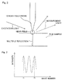
- Fig. 3 is a sketchy graph showing an interference spectrum.
- Fig. 4 is a diagram depicting the optical alignment of the near-field film-thickness measurement apparatus according to the present embodiment.
- Fig. 5 is a graph showing the results obtained by measuring a film-thickness distribution with the near-field film-thickness measurement apparatus according to the present embodiment.
- Figs. 6A, 6B, and 6C are graphs showing the spectra obtained at different positions of a film sample.
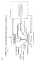
- Fig. 1 roughly shows the configuration of a film-thickness measurement apparatus 10 according to an embodiment of the present invention.
- the film-thickness measurement apparatus 10 in Fig. 1 includes a scattering near-field probe 12, a light source 14 for emitting excitation light for generating a near-field, a spectroscope 16 for wavelength scanning, a detector 18 for detecting the light scattered by the tip of the near-field probe 12 as measurement light, and a film-thickness calculating unit 20 for calculating the film thickness of a film sample from the spectrum of the measurement light.
- the excitation light emitted from the light source 14 passes through the spectroscope 16 for wavelength scanning and irradiates the tip of the near-field probe 12 and/or the surface of the film sample.
- Near-field light that is localized near the tip of the near-field probe 12 and/or on the surface of the film sample is generated by the irradiated excitation light.
- the tip of the near-field probe 12 is brought close to the surface of the film sample so that the surface of the film sample is located within the near-field region generated in the vicinity of the tip of the near-field probe 12 or so that the tip of the near-field probe 12 is located within the near-field region generated in the vicinity of the surface of the sample film, and the measurement light generated by scattering of the near-field light is detected with the detector 18.
- a signal from the detector 18 is sent to a computer 22, and the film thickness of the film sample is obtained by the film-thickness calculating unit 20 inside the computer 22 from the spectral information of the measurement light.
- the film-thickness calculating unit 20 is realized by a program that the computer 22 executes.
- the near-field probe 12 which is of the scattering type, is tapered at the tip thereof so that the radius of curvature of the tip is equal to or less than the wavelength of light.
- a probe formed of dielectric material or metal, or a probe formed by processing an optical fiber or the like to coat a metallic film, such as a gold film, on the surface thereof is generally used.
- the distance between the tip of the near-field probe 12 and the sample surface is controlled using a probe control mechanism 24. This distance control is carried out based on shear-force control or the like.
- an infrared light source is used as the light source 14
- an interferometer is used as the spectroscope 16
- Fourier transform spectrometry is employed.
- the present embodiment is not limited thereto, and another type of spectroscope may be used.
- the present embodiment has a configuration in which the spectroscope 16 is disposed in the optical path between the light source 14 and the film sample, it may have a configuration in which the spectroscope 16 is disposed in the optical path between the film sample and the detector 18.
- an incoherent light source for example, an incandescent light source or a halogen light source
- a coherent light source such as a pulsed laser
- problems such as burning of the sample, if the sample is an ordinary organic material, because the light intensity of the pulses is extremely high.
- an incoherent light source however, such problems do not arise, and it is thus possible to carry out non-contact, non-destructive measurement regardless of the type of sample.
- the measurement light from the vicinity of the tip of the near-field probe 12 is detected by the detector 18, and the detection signal is sent to the computer 22.
- the detection signal (interferogram data) is Fourier transformed to obtain spectral data for the measurement light. Based on this spectral data, the film thickness of the sample is determined in the film-thickness calculating unit 20.
- the film sample is mounted on a sample stage 26.
- the sample stage 26 is mounted on an XYZ stage (moving mechanism) 28 for moving the tip position of the near-field probe 12 over the surface of the film sample.
- a film-thickness distribution is measured by moving the tip position of the near-field probe 12 to change the measurement position on the surface of the film sample.
- the embodiment described above has a reflection configuration in which the excitation light is irradiated onto the tip of the near-field probe 12 and/or the surface of the sample from the same side as the near-field probe 12, the embodiment is not limited to this configuration.
- a transmission configuration in which the tip of the near-field probe 12 is illuminated from the rear surface of the sample or a total-reflection transmission configuration in which the tip of the near-field probe 12 is illuminated by total reflection from the rear surface of the sample may be used.
- near-field light that is localized at the tip portion is generated.
- the near-field probe 12 when the near-field probe 12 is brought close to the surface of the film sample and the surface of the film sample enters the near-field region at the tip, the near-field light in the vicinity of the probe tip is scattered and is converted to light that can propagate.
- This propagating light is oriented in all directions, but of this light, only the light propagating directly downwards (that is, in the direction perpendicular to the film sample) the near-field probe 12 experiences multiple reflections inside the film sample (at the upper and lower surfaces of the film sample), as indicated by the double-sided arrow in Fig. 2.
- light leaking out from the film surface is re-scattered at the tip of the near-field probe 12 and is directed towards the detector 18.
- This light is detected by the detector 18 as measurement light.
- This measurement light includes information about the light that underwent repeated multiple reflections in the vertical direction inside the film; therefore, by analyzing its spectrum, it is possible to obtain information about the film thickness.
- the light which is not normal to the film sample is repeatedly reflected inside the film sample but does not reach the detector 18.
- the measurement light described above is detected at the detector 18, and the detection signal is sent to the computer 22.
- predetermined data processing is performed on the detection signal to obtain the spectrum of the measurement light, as described above.
- the film thickness of the film sample is determined by the film-thickness calculating unit 20 from the spectral information.
- predetermined filtering processing is carried out on the measurement light spectrum to extract an interference spectrum component, and the film thickness is determined from the period of this interference spectrum.
- the calculation of the film thickness described above may be based on known techniques in the art (for example, see Japanese Unexamined Patent Application Publication No. H05-302816 and Japanese Unexamined Patent Application Publication No. H07-4922). For example, the film thickness is obtained from the interference spectrum shown roughly in Fig.
- the film thickness d can be obtained from equation (2) shown below.
- d N 2 n ⁇ ⁇ ⁇
- N is the number of valleys (minimal points) between the wave numbers ⁇ 1 and ⁇ 2 described above
- n is the refractive index of the film sample.
- a scattering probe is used in the present embodiment, and furthermore, by suitably designing the optical alignment, the above-described background can be significantly reduced.
- Fig. 4 is a diagram depicting the optical alignment of the near-field film-thickness measurement apparatus of the present embodiment.
- Fig. 4 shows the optical alignment of the light source 14 (and the spectroscope 16), the near-field probe 12, and the detector 18, as viewed from the probe axis direction.
- the problems described above occur when the light source, the probe tip, and the detector are aligned in a straight line.
- an aperture portion of the probe functions as both an illumination part and a light-collecting part (detector), and the probe aperture (illumination part), the film sample, and the probe aperture (light-collecting part) are arranged in a straight line.
- the detector 18 is disposed at a dark field position with respect to the positional relationship between the light source 14 and the tip of the near-field probe 12, as shown in Fig. 4. That is, the detector 18 is disposed such that the light source 14 and the detector 18 are not in a specular-reflection positional relationship with respect to the film sample (or the tip of the near-field probe 12).
- the detector 18 When using a transmission configuration in which the excitation light is irradiated from the rear surface of the sample, the detector 18 needs to be disposed at a position where the light transmitted through the film sample is not directly incident on the detector 18.
- the detector 18 As shown in Fig. 4, viewed from the probe axis direction, the detector 18 is disposed so that the line joining the detector 18 and the tip of the near-field probe 12 is perpendicular to the line joining the light source 14 and the tip of the near-field probe 12.
- the background does not enter the detector 18, and therefore, it is possible to detect, with good sensitivity, only the measurement light, containing interference information, which is generated in the vicinity of the tip of the near-field probe 12.
- interference light that departs from the direction orthogonal to the film does not enter the detector 18, and therefore, only interference light in exactly the normal-incidence direction with respect to the film is detected (with a degree of angular error allowed for in the magnitude of the radius of curvature of the probe tip).
- the film thickness can be measured with superior accuracy.
- the range of wave numbers transmittable by the optical fibers which is likely to be imposed on aperture-type probes, and it is possible to obtain the spectrum over a wide range of wave numbers. More specifically, for a small film thickness, the interference period of the interference spectrum is long, it may be unable to measure it in the range of measurement wave numbers of the aperture-type probes.
- a scattering probe such as that used in the present embodiment, because it is possible to measure the interference spectrum over a wide range of wavelengths, there is no such restriction.
- Fig. 5 is a mapping diagram showing the results of measuring the film-thickness distribution with the near-field film-thickness measurement apparatus described above.
- the film-thickness distribution is displayed in a color-coded manner.
- Figs. 6A, 6B, and 6C show measurement spectra obtained at points A, B, and C, respectively, in the mapping diagram in Fig. 5.
- the mapping diagram in Fig. 5 shows the film-thickness distribution in a 10x10 ⁇ m region of the surface of the film sample, in which mica particles are dispersed in an organic solvent.
- An interference spectrum is extracted from the spectrum for each point (see Figs. 6A to 6C), and the film thickness is calculated assuming an average refractive index n of 1.5 for the film sample.
- the spatial resolution is of the same order as the diameter of the probe tip, and it is possible to measure the film-thickness distribution with a high spatial resolution of several micrometers or less, which is smaller than the wavelength of the light used.
- using near-field optics enables measurement of the film-thickness distribution with a spatial resolution exceeding the diffraction limit of light. Furthermore, with the present embodiment, because a scattering near-field probe is employed, it is possible to perform film-thickness measurement with superior accuracy.
Landscapes
- Physics & Mathematics (AREA)
- General Physics & Mathematics (AREA)
- Chemical & Material Sciences (AREA)
- Nuclear Medicine, Radiotherapy & Molecular Imaging (AREA)
- Engineering & Computer Science (AREA)
- Nanotechnology (AREA)
- Health & Medical Sciences (AREA)
- General Health & Medical Sciences (AREA)
- Radiology & Medical Imaging (AREA)
- Crystallography & Structural Chemistry (AREA)
- Analytical Chemistry (AREA)
- Life Sciences & Earth Sciences (AREA)
- Biophysics (AREA)
- Optics & Photonics (AREA)
- Length Measuring Devices By Optical Means (AREA)
Applications Claiming Priority (1)
| Application Number | Priority Date | Filing Date | Title |
|---|---|---|---|
| JP2004380175A JP4520846B2 (ja) | 2004-12-28 | 2004-12-28 | 近接場膜厚測定装置 |
Publications (3)
| Publication Number | Publication Date |
|---|---|
| EP1677093A2 true EP1677093A2 (de) | 2006-07-05 |
| EP1677093A3 EP1677093A3 (de) | 2006-09-27 |
| EP1677093B1 EP1677093B1 (de) | 2008-09-24 |
Family
ID=36000933
Family Applications (1)
| Application Number | Title | Priority Date | Filing Date |
|---|---|---|---|
| EP05112757A Expired - Lifetime EP1677093B1 (de) | 2004-12-28 | 2005-12-22 | Nahfeldmessgerät für Filmdicke |
Country Status (4)
| Country | Link |
|---|---|
| US (1) | US20060164638A1 (de) |
| EP (1) | EP1677093B1 (de) |
| JP (1) | JP4520846B2 (de) |
| DE (1) | DE602005009917D1 (de) |
Cited By (1)
| Publication number | Priority date | Publication date | Assignee | Title |
|---|---|---|---|---|
| ITBO20080706A1 (it) * | 2008-11-24 | 2010-05-25 | Marposs Spa | Metodo e apparecchiatura per la misura ottica mediante interferometria dello spessore di un oggetto |
Families Citing this family (5)
| Publication number | Priority date | Publication date | Assignee | Title |
|---|---|---|---|---|
| US8089630B2 (en) * | 2008-03-14 | 2012-01-03 | The Board Of Trustees Of The University Of Illinois | Spectral near-field optical tomography |
| US7978343B2 (en) * | 2008-03-21 | 2011-07-12 | The Board Of Trustees Of The University Of Illinois | Nanoscale optical tomography based on volume-scanning near-field microscopy |
| JP2010139306A (ja) * | 2008-12-10 | 2010-06-24 | Shoichi Shimada | 測定装置 |
| CN105606849A (zh) * | 2016-03-01 | 2016-05-25 | 广州市刑事科学技术研究所 | 硅藻检验样品盒 |
| CN118824833B (zh) * | 2024-09-14 | 2024-12-17 | 杭州积海半导体有限公司 | 一种干法刻蚀设备 |
Family Cites Families (10)
| Publication number | Priority date | Publication date | Assignee | Title |
|---|---|---|---|---|
| JP3196945B2 (ja) * | 1992-10-23 | 2001-08-06 | 有限会社千里応用計測研究所 | 走査型光学顕微装置 |
| JP2001153785A (ja) * | 1999-11-29 | 2001-06-08 | Olympus Optical Co Ltd | 走査型近接場光学顕微鏡 |
| JP4379758B2 (ja) * | 2000-11-13 | 2009-12-09 | 日本分光株式会社 | 近接場顕微鏡 |
| JP2002267418A (ja) * | 2001-03-09 | 2002-09-18 | Horiba Ltd | 膜厚測定装置 |
| JP5288672B2 (ja) * | 2001-07-11 | 2013-09-11 | 株式会社ニコン | 表面欠陥検査装置 |
| JP2003108228A (ja) * | 2001-09-28 | 2003-04-11 | Jasco Corp | 位置決め装置、並びにそれを用いた近接場顕微鏡及び近接場分光装置。 |
| JP2003279461A (ja) * | 2002-03-25 | 2003-10-02 | Japan Science & Technology Corp | プローブ及びその製造方法 |
| JP2004125454A (ja) * | 2002-09-30 | 2004-04-22 | Jasco Corp | 近接場分光装置及び光ファイバプローブの作成方法 |
| JP2004264118A (ja) * | 2003-02-28 | 2004-09-24 | Toyota Motor Corp | 薄膜のその場解析方法および装置 |
| TWI335417B (en) * | 2003-10-27 | 2011-01-01 | Zygo Corp | Method and apparatus for thin film measurement |
-
2004
- 2004-12-28 JP JP2004380175A patent/JP4520846B2/ja not_active Expired - Fee Related
-
2005
- 2005-12-22 DE DE602005009917T patent/DE602005009917D1/de not_active Expired - Lifetime
- 2005-12-22 EP EP05112757A patent/EP1677093B1/de not_active Expired - Lifetime
- 2005-12-27 US US11/318,781 patent/US20060164638A1/en not_active Abandoned
Cited By (1)
| Publication number | Priority date | Publication date | Assignee | Title |
|---|---|---|---|---|
| ITBO20080706A1 (it) * | 2008-11-24 | 2010-05-25 | Marposs Spa | Metodo e apparecchiatura per la misura ottica mediante interferometria dello spessore di un oggetto |
Also Published As
| Publication number | Publication date |
|---|---|
| DE602005009917D1 (de) | 2008-11-06 |
| EP1677093A3 (de) | 2006-09-27 |
| EP1677093B1 (de) | 2008-09-24 |
| JP2006184200A (ja) | 2006-07-13 |
| JP4520846B2 (ja) | 2010-08-11 |
| US20060164638A1 (en) | 2006-07-27 |
Similar Documents
| Publication | Publication Date | Title |
|---|---|---|
| KR101161881B1 (ko) | 투명 기판의 결함 검출 검사장치 | |
| CN109001207B (zh) | 一种透明材料表面及内部缺陷的检测方法和检测系统 | |
| JP5841475B2 (ja) | 低コヒーレンス光源を用いた動的光散乱測定法及び動的光散乱測定装置 | |
| US6992770B2 (en) | Sensor utilizing attenuated total reflection | |
| US7218803B1 (en) | Microsphere probe for optical surface microscopy and method of using the same | |
| EP1677093B1 (de) | Nahfeldmessgerät für Filmdicke | |
| JP3196945B2 (ja) | 走査型光学顕微装置 | |
| US7016046B2 (en) | Interferometer arrangement and interferometric measuring method | |
| HUT62098A (en) | Method for testing transparent and/or reflective objects placed in the near filed by means of microscope, as well as scanning microscope | |
| JP3779352B2 (ja) | 赤外顕微分光分析方法及び装置 | |
| US11486694B2 (en) | Chromatic range sensor system for measuring workpiece thickness | |
| JPH06294629A (ja) | 表面の曲率の測定装置 | |
| US7742171B2 (en) | Reflectivity/emissivity measurement probe insensitive to variations in probe-to-target distance | |
| Bai et al. | Measuring the speed of a surface plasmon | |
| EP1476740B1 (de) | Verfahren und gerät zur überprüfung des betriebes eines optischen scanners | |
| JPS63295945A (ja) | 光沢度測定装置 | |
| US20020175690A1 (en) | Reflectometer arrangement and method for determining the reflectance of selected measurement locations of measurement objects reflecting in a spectrally dependent manner | |
| JP2544428B2 (ja) | 応力測定方法及び応力測定装置 | |
| RU2491533C1 (ru) | Способ определения глубины проникновения поля терагерцовых поверхностных плазмонов в окружающую среду | |
| RU2156437C2 (ru) | Устройство для определения шероховатости поверхности | |
| JPH08210975A (ja) | 反射光測定装置 | |
| JPS6316232A (ja) | レ−ザビ−ム径の測定方法 | |
| JP3230977B2 (ja) | 光波干渉装置の被検体ポジショニング装置 | |
| JP2003065934A (ja) | プローブ開口作製装置、及びそれを用いた近接場光学顕微鏡 | |
| FI75051B (fi) | Foerfarande och anordning foer kontaktloes bestaemning av ytkvaliteten hos ett roerligt material. |
Legal Events
| Date | Code | Title | Description |
|---|---|---|---|
| PUAI | Public reference made under article 153(3) epc to a published international application that has entered the european phase |
Free format text: ORIGINAL CODE: 0009012 |
|
| AK | Designated contracting states |
Kind code of ref document: A2 Designated state(s): AT BE BG CH CY CZ DE DK EE ES FI FR GB GR HU IE IS IT LI LT LU LV MC NL PL PT RO SE SI SK TR |
|
| AX | Request for extension of the european patent |
Extension state: AL BA HR MK YU |
|
| PUAL | Search report despatched |
Free format text: ORIGINAL CODE: 0009013 |
|
| AK | Designated contracting states |
Kind code of ref document: A3 Designated state(s): AT BE BG CH CY CZ DE DK EE ES FI FR GB GR HU IE IS IT LI LT LU LV MC NL PL PT RO SE SI SK TR |
|
| AX | Request for extension of the european patent |
Extension state: AL BA HR MK YU |
|
| RIC1 | Information provided on ipc code assigned before grant |
Ipc: G01N 13/14 20060101AFI20060327BHEP Ipc: G01B 11/06 20060101ALI20060821BHEP Ipc: G12B 21/06 20060101ALI20060821BHEP |
|
| 17P | Request for examination filed |
Effective date: 20070327 |
|
| AKX | Designation fees paid |
Designated state(s): DE FR GB |
|
| GRAP | Despatch of communication of intention to grant a patent |
Free format text: ORIGINAL CODE: EPIDOSNIGR1 |
|
| GRAS | Grant fee paid |
Free format text: ORIGINAL CODE: EPIDOSNIGR3 |
|
| GRAA | (expected) grant |
Free format text: ORIGINAL CODE: 0009210 |
|
| AK | Designated contracting states |
Kind code of ref document: B1 Designated state(s): DE FR GB |
|
| REG | Reference to a national code |
Ref country code: GB Ref legal event code: FG4D |
|
| REF | Corresponds to: |
Ref document number: 602005009917 Country of ref document: DE Date of ref document: 20081106 Kind code of ref document: P |
|
| PLBE | No opposition filed within time limit |
Free format text: ORIGINAL CODE: 0009261 |
|
| STAA | Information on the status of an ep patent application or granted ep patent |
Free format text: STATUS: NO OPPOSITION FILED WITHIN TIME LIMIT |
|
| 26N | No opposition filed |
Effective date: 20090625 |
|
| PGFP | Annual fee paid to national office [announced via postgrant information from national office to epo] |
Ref country code: FR Payment date: 20110104 Year of fee payment: 6 |
|
| PGFP | Annual fee paid to national office [announced via postgrant information from national office to epo] |
Ref country code: GB Payment date: 20101221 Year of fee payment: 6 |
|
| PGFP | Annual fee paid to national office [announced via postgrant information from national office to epo] |
Ref country code: DE Payment date: 20101222 Year of fee payment: 6 |
|
| GBPC | Gb: european patent ceased through non-payment of renewal fee |
Effective date: 20111222 |
|
| REG | Reference to a national code |
Ref country code: FR Ref legal event code: ST Effective date: 20120831 |
|
| REG | Reference to a national code |
Ref country code: DE Ref legal event code: R119 Ref document number: 602005009917 Country of ref document: DE Effective date: 20120703 |
|
| PG25 | Lapsed in a contracting state [announced via postgrant information from national office to epo] |
Ref country code: DE Free format text: LAPSE BECAUSE OF NON-PAYMENT OF DUE FEES Effective date: 20120703 Ref country code: GB Free format text: LAPSE BECAUSE OF NON-PAYMENT OF DUE FEES Effective date: 20111222 |
|
| PG25 | Lapsed in a contracting state [announced via postgrant information from national office to epo] |
Ref country code: FR Free format text: LAPSE BECAUSE OF NON-PAYMENT OF DUE FEES Effective date: 20120102 |