EP1677385B1 - Elektronisch gesteuerte breitbandige Antenne - Google Patents
Elektronisch gesteuerte breitbandige Antenne Download PDFInfo
- Publication number
- EP1677385B1 EP1677385B1 EP05112055A EP05112055A EP1677385B1 EP 1677385 B1 EP1677385 B1 EP 1677385B1 EP 05112055 A EP05112055 A EP 05112055A EP 05112055 A EP05112055 A EP 05112055A EP 1677385 B1 EP1677385 B1 EP 1677385B1
- Authority
- EP
- European Patent Office
- Prior art keywords
- antenna
- wave
- guide
- frequency
- reflector panel
- Prior art date
- Legal status (The legal status is an assumption and is not a legal conclusion. Google has not performed a legal analysis and makes no representation as to the accuracy of the status listed.)
- Expired - Lifetime
Links
Images

Classifications
-
- H—ELECTRICITY
- H01—ELECTRIC ELEMENTS
- H01Q—ANTENNAS, i.e. RADIO AERIALS
- H01Q3/00—Arrangements for changing or varying the orientation or the shape of the directional pattern of the waves radiated from an antenna or antenna system
- H01Q3/22—Arrangements for changing or varying the orientation or the shape of the directional pattern of the waves radiated from an antenna or antenna system varying the orientation in accordance with variation of frequency of radiated wave
-
- H—ELECTRICITY
- H01—ELECTRIC ELEMENTS
- H01Q—ANTENNAS, i.e. RADIO AERIALS
- H01Q19/00—Combinations of primary active antenna elements and units with secondary devices, e.g. with quasi-optical devices, for giving the antenna a desired directional characteristic
- H01Q19/10—Combinations of primary active antenna elements and units with secondary devices, e.g. with quasi-optical devices, for giving the antenna a desired directional characteristic using reflecting surfaces
- H01Q19/18—Combinations of primary active antenna elements and units with secondary devices, e.g. with quasi-optical devices, for giving the antenna a desired directional characteristic using reflecting surfaces having two or more spaced reflecting surfaces
- H01Q19/19—Combinations of primary active antenna elements and units with secondary devices, e.g. with quasi-optical devices, for giving the antenna a desired directional characteristic using reflecting surfaces having two or more spaced reflecting surfaces comprising one main concave reflecting surface associated with an auxiliary reflecting surface
- H01Q19/195—Combinations of primary active antenna elements and units with secondary devices, e.g. with quasi-optical devices, for giving the antenna a desired directional characteristic using reflecting surfaces having two or more spaced reflecting surfaces comprising one main concave reflecting surface associated with an auxiliary reflecting surface wherein a reflecting surface acts also as a polarisation filter or a polarising device
-
- H—ELECTRICITY
- H01—ELECTRIC ELEMENTS
- H01Q—ANTENNAS, i.e. RADIO AERIALS
- H01Q3/00—Arrangements for changing or varying the orientation or the shape of the directional pattern of the waves radiated from an antenna or antenna system
- H01Q3/44—Arrangements for changing or varying the orientation or the shape of the directional pattern of the waves radiated from an antenna or antenna system varying the electric or magnetic characteristics of reflecting, refracting, or diffracting devices associated with the radiating element
- H01Q3/46—Active lenses or reflecting arrays
-
- G—PHYSICS
- G01—MEASURING; TESTING
- G01S—RADIO DIRECTION-FINDING; RADIO NAVIGATION; DETERMINING DISTANCE OR VELOCITY BY USE OF RADIO WAVES; LOCATING OR PRESENCE-DETECTING BY USE OF THE REFLECTION OR RERADIATION OF RADIO WAVES; ANALOGOUS ARRANGEMENTS USING OTHER WAVES
- G01S13/00—Systems using the reflection or reradiation of radio waves, e.g. radar systems; Analogous systems using reflection or reradiation of waves whose nature or wavelength is irrelevant or unspecified
- G01S13/88—Radar or analogous systems specially adapted for specific applications
- G01S13/89—Radar or analogous systems specially adapted for specific applications for mapping or imaging
- G01S13/90—Radar or analogous systems specially adapted for specific applications for mapping or imaging using synthetic aperture techniques, e.g. synthetic aperture radar [SAR] techniques
Definitions
- the present invention relates to an electronic scanning antenna operating over a wide frequency band. It is particularly applicable for applications requiring compact or low cost antennas.
- An electronic scanning antenna comprises a network of microwave sources each associated with a phase-shifter. It is known that the direction of the antenna beam is a function of the phase shifts applied by the phase shifters to the source signals. For a given phase shifter state and a given frequency, a well-defined antenna beam direction is obtained. However, for the same state of the phase shifters, when the transmission frequency varies there is a misalignment of the antenna beam.
- SAR the English expression Synthetic Aperture Radar
- a patent application US 2004/0164915 A1 discloses compensation for misalignment of an antenna beam by varying the frequency variation of the wave passing through the slot guide.
- the direction of travel of the microwave wave in the guide depends on the direction of the pointing ⁇ p of the wave reflected by the panel.
- the antenna comprises for example a switch having at least one input and two outputs, a first output being connected by a microwave line to an input of the slot guide and a second output being connected by a microwave line to the another input of the guide, the switch receiving the input microwave wave and switching its input to one of the two outputs according to the pointing direction ⁇ p .
- the slot guide is placed at the level of the reflector panel so that the slots are arranged in the plane of the array of phase shift cells, the wave emitted by the guide being reflected by a network of conducting wires towards the reflector panel.
- a second slotted guide is for example arranged next to the slotted guide to form two beams of a monopulse antenna.
- the slot guide is for example corrugated.
- the main advantages of the invention are that it makes it possible to produce a small antenna, that it can be used in many applications and that it is economical.
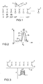
- the figure 1 recalls the principle of operation of an electronic scanning antenna.
- the antenna comprises a network of microwave sources 1 or radiating elements. Each element 1 is connected to a phase-shifter 2. On transmission, the microwave signals intended to be emitted by the sources are first phase-shifted by the phase-shifters 2 according to a well-established law which defines the pointing direction 3 of the beam. antenna. This direction 3 is defined by a pointing angle ⁇ p with respect to the axis 4 of the antenna, direction 4 perpendicular to the plane of the antenna.
- the network represented by the figure 1 is linear, but it also represents a plane network where each source represents in fact an element of a line of the network where all the sources of this line have the same phase shift.
- the first line represented by the first source of the network of the figure 1 a zero phase shift or a reference phase shift. Then the phase is incremented by a phase shift ⁇ from one source to the next, or from one line to the next.
- the first source has a zero phase shift
- the second source has a phase shift of ⁇
- the third source has a phase shift of 2 ⁇
- so on up to the nth source which has a shift of (n - 1) ⁇ .
- the figure 2 illustrates the lobe of the antenna of the figure 1 for a pointing angle ⁇ p as defined by the relation (1) for a first antenna frequency f 1 , this frequency being that of a signal on transmission or reception.
- c the speed of light.
- This antenna lobe is represented by a first curve 21 centered on the angle ⁇ p in a system of axes where the ordinates represent the microwave power and where the abscissa represent the angles with respect to the axis 4 of the antenna , the latter corresponding to the angle 0.
- the curve 21 illustrates a conventional antenna lobe, with its main lobe 22 flanked by its sidelobes 23.
- the figure 2 illustrates by a second curve 24 the antenna lobe for a second antenna frequency f 2 .
- the two lobes 21, 24, one at the frequency f 1 , the other at the frequency f 2 are offset by ⁇ p .
- this antenna comprises an array of radiating elements 1 controlled by phase shifters 2.
- a microwave signal at the frequency f feeds the radiating elements 1 via the phase shifters 2 via a distribution circuit 31.
- the frequency f traverses a frequency band ⁇ F whose width is for example of the order of 1 GHz. With a bandwidth of this order, a SAR-type radar can deliver synthetic images having a resolution of about 20 cm. Frequency variations within this ⁇ F band cause scattering of the antenna pointing as illustrated by the figure 2 .
- the antenna is no longer directive but dispersive.
- ⁇ ⁇ F 360 sin ⁇ p ⁇ Max ⁇ x ⁇
- ⁇ F in megahertz (MHz) and L in meters (m).
- delay lines These are real delay lines that are used, not just phase shifters. However these lines with delays induce losses. So we have to compensate for these losses by amplifiers.
- the antenna structure is more complex, larger and more expensive.
- the figure 4 present in a sectional view an embodiment of an antenna according to the invention.
- This antenna uses a reflection panel with phase shift cells used in particular in the type of "reflect array” or “transmit array” type antennas.
- the antenna comprises at least one slotted microwave waveguide 41 and a microwave reflective panel 42, the slot guide 41 acting as an illuminator.
- the reflector panel 42 also called “reflect array” in the Anglo-Saxon literature is a network of electronically controllable phase shifters.
- An example of reflector panel is notably presented in the French patent application published under the number 2,786,610 . Examples of microwave reflective panels or "reflect array” are still described in the French patent applications published under the numbers 2,789,521 , 2,801,729 and 2,812,457 .
- a primary source illuminates the reflector network. It emits microwave waves to the reflector panel.
- This panel comprises a network of elementary cells performing the reflection and phase shift of the waves they receive. By controlling the phase shifts printed on the wave received by each cell, it is possible, as is known, to form a microwave beam in a desired direction.
- the control principle of the antenna beam is the same as in the examples described in Figures 1 and 3 except that a microwave signal is out of phase at the moment of its reflection on the panel.
- the slot guide 41 is powered by a microwave wave in progressive mode. It radiates a microwave wave 43 to the reflector panel 42. In the particular embodiment of the figure 4 , the slits of the guide 41 are in the plane of the reflector panel 42.
- the waves 43 emitted by the slots are then reflected for example by a panel 44 with conducting wires to the panel 42.
- the waves 43 are then reflected by the panel with phase-shifts as described above before crossing the son network 44.
- the structure of such a panel is known as the "transmit array” Anglo-Saxon.
- Such an antenna according to the invention makes it possible to compensate for antenna beam misalignments due to frequency variations without, in particular, using delay lines. It therefore has a structure that is not complex.
- the lack of dispersion of an electronic scanning antenna is compensated for by another defect.
- This defect is a defect in a slotted guide as an illuminator.
- the figure 5 shows an example of slot guide 41 which can be used in an antenna according to the invention for illuminating the reflector panel 42.
- the slotted guide 41 has a width a and a height h. Slots 55 are arranged on one side of width a. The pitch between the centers of two successive slits is equal to d.
- the guide is powered by a frequency wave f in progressive mode.
- the electrical component E of the electromagnetic field is parallel to the side of width a.
- the example of a guide to figure 5 is a flat guide, i.e., h is less than a.
- a slotted guide has a defect that is illustrated by the figure 5 .
- the relation (6) shows that sin ( ⁇ f ) decreases when ⁇ increases. In other words, the angle ⁇ f increases with the frequency f feeding the slotted guide 41.
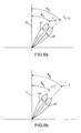
- the figure 6a illustrates two emission beams 61, 62 for two waves emitted by the slotted guides, one at the frequency f 1 and the other at the frequency f 2 , f 2 being greater than f 1 .
- the first beam 61 corresponding to the first frequency f 1 makes an angle ⁇ f1 with respect to the axis 52 of the guide to slots.
- the second beam 62 corresponding to the second frequency f 2 makes an angle ⁇ f2 with respect to this same axis 52.
- the angle ⁇ f2 is greater than the angle ⁇ f1 .
- the figure 6b illustrates the misalignment of an antenna beam with respect to a reference axis 4, misalignment due to the frequency variation.
- This misalignment may concern an antenna as schematically illustrated by the Figures 1 and 3 . It also relates, and for the same physical reasons, a reflector panel of the type used in an antenna according to the invention.
- the figure 6b has two beams 63, 64, for the two frequencies f 1 , f 2 below.
- the first beam 63 corresponding to the first frequency f 1 makes an angle ⁇ p1 with respect to the reference axis 4.
- the second beam 64 corresponding to the second frequency f 2 makes an angle ⁇ p2 with respect to this same axis 4.
- the beam pointing angle decreases as the frequency increases.
- the pointing angle ⁇ p of the reflector panel 42 therefore varies in a manner opposite to the deflection angle ⁇ f of the slot guide 41.
- figure 6b shows that the angle ⁇ p2 is smaller than the angle ⁇ p1 .
- the figure 7 presents only the illuminating part of an antenna according to the invention in an embodiment which takes into account the direction of misalignment.
- the direction of misalignment is positive when ⁇ p is positive and the direction of misalignment is negative when ⁇ p is negative.
- the direction of misalignment changes direction it is not the same for the deviation ⁇ f .
- an antenna according to the invention may comprise a switch, for example electromechanical 61.
- This switch 61 has an input which receives the wave at the frequency f. It also has two outputs. A first output is connected by a microwave line to an input 62 of the slot guide 41 and a second output is connected by a microwave line to the other input 63 of the slot guide.
- the switch switches the input signal from one output to the other depending on the direction of misalignment ⁇ p .
- the switch 61 is for example controlled by a control unit which also controls the phase shift of the cells of the reflector panel 42. In particular this control unit, which controls the pointing angle ⁇ p , actually knows its sign and can therefore control the switching of the switch 61 accordingly .
- the illuminator constituted by the slot guide 41
- the slot guide 41 is therefore placed at the level of the reflector panel 42. More particularly, the outputs of the slots of the guide are in the plane of the network of the cells. of phase shifts of the reflector panel.
- the slot guide 41 illuminates the reflecting panel by reflection on a network of conducting wires 44.
- the network of wires is placed opposite the reflector panel 42 and parallel thereto.
- the network of son is for example placed at a distance of a few centimeters from the reflector panel.
- the wave 43 emitted by the slots is reflected by the network of son and then it is reflected again on the reflector panel 42 in a direction depending on the phase shifts applied by the cells.
- the pointing variation ⁇ p created by the variations of the frequency f of the wave 43 is partially compensated by the deviation ⁇ f of this same wave 43 at the output of the slot guide.
- the wave After reflection on the reflector panel 42 the wave passes through the wire network 44.
- the direction of the antenna beam thus created depends on the control of the phase shifters, the variation of pointing function of the frequency being partially corrected as indicated above.
- the network of wires 44 is designed to reflect the wave 43 at the exit of the slot guide and to allow the wave to pass after reflection on the reflector panel 42.
- the wires are, for example, perpendicular to the electric field E of the wave 43.
- E electric field
- a rotation of ⁇ / 2 is applied to this field E. It then becomes parallel to the conductor son of the network 44.
- the wave reflected by the panel 42 then passes through the network of wires 44.
- the means which make it possible to maintain the network of wires 44 integral with the reflector panel 42 are not represented on the figure 4 .
- Several modes of attachment can be used.
- the son network itself being disposed on a panel of dielectric material, this panel can be secured to the reflector panel by spacers for example.
- the network of son is for example printed on the dielectric panel in a printed circuit technology.
- the exemplary embodiment of the figure 4 is of type "transmit array".
- This embodiment has the particular advantage of being compact, so space-saving. It would of course be possible to make a "reflect array” antenna. In this case the illuminator is no longer placed at the reflective plane. The slot guide 41 is then placed opposite the reflector panel.
- the "reflect array” type solution may be less advantageous than the "transmit array” solution because in this embodiment the slotted guide 41 hides the reflector panel at the front, in the field of emission or reception of the antenna.
- the slotted guide hides part of the phase-shifting network or rather it removes part of it.
- corrugated slotted guide is a slotted guide that has a protrusion on the inside. His interest is in particular to have a lower cutoff frequency and therefore to have a smaller width, which decreases the mask of the illuminator.
- an antenna according to the invention thus makes it possible to avoid the use of delay lines to compensate for antenna misalignments due to frequency variations. It therefore allows a compact and inexpensive embodiment.
- an antenna as illustrated by the figure 4 may have a small thickness. In X-band for example, the thickness does not exceed ten centimeters for a dimension of 1, 5 meters x 1, 5 meters. Due in particular to its performance, its small size and its low cost, an antenna according to the invention can be used for many applications. In particular it can be used on drones, for example for radar imaging SAR type applications. It can also be used for radar imagery applied to surveillance, for example for monitoring air corridors at major airports.
Landscapes
- Variable-Direction Aerials And Aerial Arrays (AREA)
- Aerials With Secondary Devices (AREA)
- Waveguide Aerials (AREA)
Claims (5)
- Antenne mit elektronischer Abtastung, die wenigstens Folgendes umfasst:- eine Reflektorplatte (42), die eine Anordnung von Phasenverschiebungszellen umfasst;- einen Schlitzwellenleiter (41), der die Ablenkplatte (42) mit einer Ultrahochfrequenzwelle (43) mit einer variablen Frequenz f beleuchtet;wobei die Abweichung Δθf von der Richtung (51) der von der von dem Schlitzwellenleiter emittierten Welle (43) in Abhängigkeit von der Frequenzvariation der Variation Δθp der Zeigerichtung der von der Reflektorplatte (42) reflektierten Welle (43) entgegengesetzt ist, dadurch gekennzeichnet, dass die Laufrichtung der Ultrahochfrequenzwelle im Leiter (41) von der Zeigerichtung (θp) der von der Platte (42) reflektierten Welle (43) abhängig ist, wobei die Antenne einen Schalter (61) mit wenigstens einem Eingang und zwei Ausgängen umfasst, wobei ein erster Ausgang durch eine Ultrahochfrequenzleitung mit einem Eingang (62) des Schlitzleiters (41) verbunden ist und ein zweiter Ausgang durch eine Ultrahochfrequenzleitung mit dem anderen Eingang (63) des Leiters verbunden ist, wobei der Schalter am Eingang die Ultrahochfrequenzwelle empfängt und seinen Eingang auf einen von zwei Ausgängen in Abhängigkeit von der Zeigerichtung (θp) schaltet.
- Antenne nach Anspruch 1, dadurch gekennzeichnet, dass der Leiter (41) so auf der Reflektorplatte (42) platziert ist, dass die Schlitze in der Ebene der Anordnung von Phasenverschiebungszellen angeordnet sind, wobei die von dem Leiter emittierte Welle (43) von einer Anordnung von Leitungsdrähten (44) zur Reflektorplatte (42) reflektiert wird.
- Antenne nach einem der vorherigen Ansprüche, dadurch gekennzeichnet, dass ein zweiter Schlitzleiter auf der Seite des Schlitzleiters (41) angeordnet ist, um zwei Strahlen einer Monopulsantenne zu bilden.
- Antenne nach einem der vorherigen Ansprüche, dadurch gekennzeichnet, dass der Schlitzleiter (41) gewellt ist.
- Antenne nach einem der vorherigen Ansprüche, dadurch gekennzeichnet, dass sie für Radaranwendungen mit synthetischer Bildgebung des SAR-Typs verwendet wird.
Applications Claiming Priority (1)
| Application Number | Priority Date | Filing Date | Title |
|---|---|---|---|
| FR0413343A FR2879359B1 (fr) | 2004-12-15 | 2004-12-15 | Antenne a balayage electronique large bande |
Publications (2)
| Publication Number | Publication Date |
|---|---|
| EP1677385A1 EP1677385A1 (de) | 2006-07-05 |
| EP1677385B1 true EP1677385B1 (de) | 2013-02-20 |
Family
ID=34954988
Family Applications (1)
| Application Number | Title | Priority Date | Filing Date |
|---|---|---|---|
| EP05112055A Expired - Lifetime EP1677385B1 (de) | 2004-12-15 | 2005-12-13 | Elektronisch gesteuerte breitbandige Antenne |
Country Status (3)
| Country | Link |
|---|---|
| US (1) | US7495622B2 (de) |
| EP (1) | EP1677385B1 (de) |
| FR (1) | FR2879359B1 (de) |
Families Citing this family (3)
| Publication number | Priority date | Publication date | Assignee | Title |
|---|---|---|---|---|
| DE102015225578A1 (de) * | 2015-12-17 | 2017-06-22 | Robert Bosch Gmbh | Vorrichtung zum Empfangen von Mikrowellenstrahlung |
| EP3432027B1 (de) * | 2017-07-20 | 2021-09-01 | Airbus Defence and Space GmbH | Radarsystem mit synthetischer apertur mit hochauflösendem breiten streifen |
| JP7211398B2 (ja) * | 2020-05-25 | 2023-01-24 | 株式会社デンソー | 導波管スロットアンテナ |
Family Cites Families (9)
| Publication number | Priority date | Publication date | Assignee | Title |
|---|---|---|---|---|
| FR1291750A (fr) * | 1961-03-17 | 1962-04-27 | Csf | Antenne plate pour radar à impulsion unique |
| IL66327A0 (de) * | 1982-07-15 | 1982-11-30 | ||
| JPH02128168A (ja) * | 1988-11-07 | 1990-05-16 | Natl Space Dev Agency Japan<Nasda> | 電子走査型マイクロ波放射計 |
| FR2786610B1 (fr) * | 1997-02-03 | 2001-04-27 | Thomson Csf | Reflecteur hyperfrequence actif pour antenne a balayage electronique |
| DE19845870A1 (de) * | 1997-11-28 | 1999-06-02 | Daimler Benz Aerospace Ag | Reflektor-Antennenanordnung |
| FR2789521A1 (fr) * | 1999-02-05 | 2000-08-11 | Thomson Csf | Antenne a balayage electronique bi-bande, a reflecteur hyperfrequence actif |
| FR2801729B1 (fr) * | 1999-11-26 | 2007-02-09 | Thomson Csf | Reflecteur hyperfrequence actif a balayage electronique |
| FR2812457B1 (fr) * | 2000-07-28 | 2004-05-28 | Thomson Csf | Reflecteur hyperfrequence actif a bi-polarisation, notamment pour antenne a balalyage electronique |
| US6822615B2 (en) * | 2003-02-25 | 2004-11-23 | Raytheon Company | Wideband 2-D electronically scanned array with compact CTS feed and MEMS phase shifters |
-
2004
- 2004-12-15 FR FR0413343A patent/FR2879359B1/fr not_active Expired - Fee Related
-
2005
- 2005-12-13 EP EP05112055A patent/EP1677385B1/de not_active Expired - Lifetime
- 2005-12-14 US US11/302,500 patent/US7495622B2/en not_active Expired - Fee Related
Also Published As
| Publication number | Publication date |
|---|---|
| US20060244670A1 (en) | 2006-11-02 |
| US7495622B2 (en) | 2009-02-24 |
| FR2879359A1 (fr) | 2006-06-16 |
| EP1677385A1 (de) | 2006-07-05 |
| FR2879359B1 (fr) | 2007-02-09 |
Similar Documents
| Publication | Publication Date | Title |
|---|---|---|
| EP0600799B1 (de) | Aktive Antenne mit variabler Polarisations-Synthese | |
| EP2532046B1 (de) | Flachplatten-abtastantenne für landfahrzeuganwendung, fahrzeug mit einer solchen antenne und satellitentelekommunikationssystem mit solch einem fahrzeug | |
| EP0012055B1 (de) | In Streifenleitertechnik ausgeführter Monopulsprimärstrahler und Antenne mit einem solchen Strahler | |
| EP2202839B1 (de) | Kompakte Speiseeinrichtung zur Erzeugung einer Zirkularpolarisation in einer Antenne und Herstellungsvervahren einer solchen Speiseeinrichtung | |
| EP2532050B1 (de) | Bordinterne direktionale flachplattenantenne, fahrzeug mit einer solchen antenne und satellitentelekommunikationssystem mit einem solchen fahrzeug | |
| FR2886773A1 (fr) | Antenne dispersive en frequence appliquee notamment a un radar meteorologique | |
| FR2863783A1 (fr) | Dispositif et procede de dephasage | |
| EP3179551B1 (de) | Kompakteinheit zur doppelpolarisierten ansteuerung für ein strahlungselement einer antenne, und kompaktes netz, das mindestens vier kompakte ansteuerungseinheiten umfasst | |
| EP0462864B1 (de) | Vorrichtung zur Speisung von Strahlungselementen einer Gruppenantenne und ihre Verwendung für eine Antenne eines Landungshilfssystems vom Typ MLS | |
| EP3176875B1 (de) | Aufbau einer aktiven hybriden rekonfigurierbaren strahlbildungsantenne | |
| WO2014202498A1 (fr) | Source pour antenne parabolique | |
| EP3180816B1 (de) | Mehrbandige quelle mit koaxialem horn mit monopulsnachführungsverfahren für eine reflektorantenne | |
| FR3069713B1 (fr) | Antenne integrant des lentilles a retard a l'interieur d'un repartiteur a base de diviseurs a guide d'ondes a plaques paralleles | |
| CA2035111A1 (fr) | Antenne en guides d'ondes a fentes, notamment pour radars spatiaux | |
| EP0149400B1 (de) | Strahler mit einer Zirkularmoduserregungsvorrichtung | |
| EP1677385B1 (de) | Elektronisch gesteuerte breitbandige Antenne | |
| CA2385787A1 (fr) | Reflecteur hyperfrequence actif a bipolarisation, notamment pour antenne a balayage electronique | |
| EP4523291A1 (de) | Flache antenne mit zweidimensionaler elektronischer abtastung | |
| FR2930844A1 (fr) | Antenne rf d'emission et/ou de reception comportant des elements rayonnants excites par couplage electromagnetique sans contact | |
| EP1286416B1 (de) | Schliessen und Phasenverschieben einer Antenne | |
| EP0613019B1 (de) | Abweichungsantenne für Monopulsradar | |
| FR2886771A1 (fr) | Antenne dispersive en frequence appliquee notamment a un radar meteorologique. | |
| FR2697680A1 (fr) | Antenne radar à balayage électronique, notamment applicable à un radar anticollision pour automobile. | |
| FR2943466A1 (fr) | Element rayonnant a bipolarisation | |
| FR2747842A1 (fr) | Lentille hyperfrequence multibande et son application a une antenne a balayage electronique |
Legal Events
| Date | Code | Title | Description |
|---|---|---|---|
| PUAI | Public reference made under article 153(3) epc to a published international application that has entered the european phase |
Free format text: ORIGINAL CODE: 0009012 |
|
| AK | Designated contracting states |
Kind code of ref document: A1 Designated state(s): AT BE BG CH CY CZ DE DK EE ES FI FR GB GR HU IE IS IT LI LT LU LV MC NL PL PT RO SE SI SK TR |
|
| AX | Request for extension of the european patent |
Extension state: AL BA HR MK YU |
|
| 17P | Request for examination filed |
Effective date: 20061215 |
|
| 17Q | First examination report despatched |
Effective date: 20070111 |
|
| AKX | Designation fees paid |
Designated state(s): DE ES GB IT SE |
|
| GRAP | Despatch of communication of intention to grant a patent |
Free format text: ORIGINAL CODE: EPIDOSNIGR1 |
|
| GRAS | Grant fee paid |
Free format text: ORIGINAL CODE: EPIDOSNIGR3 |
|
| GRAA | (expected) grant |
Free format text: ORIGINAL CODE: 0009210 |
|
| AK | Designated contracting states |
Kind code of ref document: B1 Designated state(s): DE ES GB IT SE |
|
| REG | Reference to a national code |
Ref country code: GB Ref legal event code: FG4D Free format text: NOT ENGLISH |
|
| REG | Reference to a national code |
Ref country code: DE Ref legal event code: R096 Ref document number: 602005038194 Country of ref document: DE Effective date: 20130418 |
|
| PG25 | Lapsed in a contracting state [announced via postgrant information from national office to epo] |
Ref country code: ES Free format text: LAPSE BECAUSE OF FAILURE TO SUBMIT A TRANSLATION OF THE DESCRIPTION OR TO PAY THE FEE WITHIN THE PRESCRIBED TIME-LIMIT Effective date: 20130531 Ref country code: SE Free format text: LAPSE BECAUSE OF FAILURE TO SUBMIT A TRANSLATION OF THE DESCRIPTION OR TO PAY THE FEE WITHIN THE PRESCRIBED TIME-LIMIT Effective date: 20130220 |
|
| PLBE | No opposition filed within time limit |
Free format text: ORIGINAL CODE: 0009261 |
|
| STAA | Information on the status of an ep patent application or granted ep patent |
Free format text: STATUS: NO OPPOSITION FILED WITHIN TIME LIMIT |
|
| PG25 | Lapsed in a contracting state [announced via postgrant information from national office to epo] |
Ref country code: IT Free format text: LAPSE BECAUSE OF FAILURE TO SUBMIT A TRANSLATION OF THE DESCRIPTION OR TO PAY THE FEE WITHIN THE PRESCRIBED TIME-LIMIT Effective date: 20130220 |
|
| 26N | No opposition filed |
Effective date: 20131121 |
|
| REG | Reference to a national code |
Ref country code: DE Ref legal event code: R097 Ref document number: 602005038194 Country of ref document: DE Effective date: 20131121 |
|
| REG | Reference to a national code |
Ref country code: DE Ref legal event code: R119 Ref document number: 602005038194 Country of ref document: DE |
|
| GBPC | Gb: european patent ceased through non-payment of renewal fee |
Effective date: 20131213 |
|
| REG | Reference to a national code |
Ref country code: DE Ref legal event code: R119 Ref document number: 602005038194 Country of ref document: DE Effective date: 20140701 |
|
| PG25 | Lapsed in a contracting state [announced via postgrant information from national office to epo] |
Ref country code: DE Free format text: LAPSE BECAUSE OF NON-PAYMENT OF DUE FEES Effective date: 20140701 |
|
| PG25 | Lapsed in a contracting state [announced via postgrant information from national office to epo] |
Ref country code: GB Free format text: LAPSE BECAUSE OF NON-PAYMENT OF DUE FEES Effective date: 20131213 |