EP1679687A2 - Dispositif d'affichage et son procédé de commande - Google Patents
Dispositif d'affichage et son procédé de commande Download PDFInfo
- Publication number
- EP1679687A2 EP1679687A2 EP06100105A EP06100105A EP1679687A2 EP 1679687 A2 EP1679687 A2 EP 1679687A2 EP 06100105 A EP06100105 A EP 06100105A EP 06100105 A EP06100105 A EP 06100105A EP 1679687 A2 EP1679687 A2 EP 1679687A2
- Authority
- EP
- European Patent Office
- Prior art keywords
- signal
- signals
- shift
- period
- select
- Prior art date
- Legal status (The legal status is an assumption and is not a legal conclusion. Google has not performed a legal analysis and makes no representation as to the accuracy of the status listed.)
- Granted
Links
Images


Classifications
-
- G—PHYSICS
- G09—EDUCATION; CRYPTOGRAPHY; DISPLAY; ADVERTISING; SEALS
- G09G—ARRANGEMENTS OR CIRCUITS FOR CONTROL OF INDICATING DEVICES USING STATIC MEANS TO PRESENT VARIABLE INFORMATION
- G09G3/00—Control arrangements or circuits, of interest only in connection with visual indicators other than cathode-ray tubes
- G09G3/20—Control arrangements or circuits, of interest only in connection with visual indicators other than cathode-ray tubes for presentation of an assembly of a number of characters, e.g. a page, by composing the assembly by combination of individual elements arranged in a matrix no fixed position being assigned to or needed to be assigned to the individual characters or partial characters
- G09G3/22—Control arrangements or circuits, of interest only in connection with visual indicators other than cathode-ray tubes for presentation of an assembly of a number of characters, e.g. a page, by composing the assembly by combination of individual elements arranged in a matrix no fixed position being assigned to or needed to be assigned to the individual characters or partial characters using controlled light sources
- G09G3/30—Control arrangements or circuits, of interest only in connection with visual indicators other than cathode-ray tubes for presentation of an assembly of a number of characters, e.g. a page, by composing the assembly by combination of individual elements arranged in a matrix no fixed position being assigned to or needed to be assigned to the individual characters or partial characters using controlled light sources using electroluminescent panels
- G09G3/32—Control arrangements or circuits, of interest only in connection with visual indicators other than cathode-ray tubes for presentation of an assembly of a number of characters, e.g. a page, by composing the assembly by combination of individual elements arranged in a matrix no fixed position being assigned to or needed to be assigned to the individual characters or partial characters using controlled light sources using electroluminescent panels semiconductive, e.g. using light-emitting diodes [LED]
- G09G3/3208—Control arrangements or circuits, of interest only in connection with visual indicators other than cathode-ray tubes for presentation of an assembly of a number of characters, e.g. a page, by composing the assembly by combination of individual elements arranged in a matrix no fixed position being assigned to or needed to be assigned to the individual characters or partial characters using controlled light sources using electroluminescent panels semiconductive, e.g. using light-emitting diodes [LED] organic, e.g. using organic light-emitting diodes [OLED]
- G09G3/3225—Control arrangements or circuits, of interest only in connection with visual indicators other than cathode-ray tubes for presentation of an assembly of a number of characters, e.g. a page, by composing the assembly by combination of individual elements arranged in a matrix no fixed position being assigned to or needed to be assigned to the individual characters or partial characters using controlled light sources using electroluminescent panels semiconductive, e.g. using light-emitting diodes [LED] organic, e.g. using organic light-emitting diodes [OLED] using an active matrix
- G09G3/3233—Control arrangements or circuits, of interest only in connection with visual indicators other than cathode-ray tubes for presentation of an assembly of a number of characters, e.g. a page, by composing the assembly by combination of individual elements arranged in a matrix no fixed position being assigned to or needed to be assigned to the individual characters or partial characters using controlled light sources using electroluminescent panels semiconductive, e.g. using light-emitting diodes [LED] organic, e.g. using organic light-emitting diodes [OLED] using an active matrix with pixel circuitry controlling the current through the light-emitting element
-
- A—HUMAN NECESSITIES
- A01—AGRICULTURE; FORESTRY; ANIMAL HUSBANDRY; HUNTING; TRAPPING; FISHING
- A01K—ANIMAL HUSBANDRY; AVICULTURE; APICULTURE; PISCICULTURE; FISHING; REARING OR BREEDING ANIMALS, NOT OTHERWISE PROVIDED FOR; NEW BREEDS OF ANIMALS
- A01K93/00—Floats for angling, with or without signalling devices
-
- A—HUMAN NECESSITIES
- A01—AGRICULTURE; FORESTRY; ANIMAL HUSBANDRY; HUNTING; TRAPPING; FISHING
- A01K—ANIMAL HUSBANDRY; AVICULTURE; APICULTURE; PISCICULTURE; FISHING; REARING OR BREEDING ANIMALS, NOT OTHERWISE PROVIDED FOR; NEW BREEDS OF ANIMALS
- A01K95/00—Sinkers for angling
-
- G—PHYSICS
- G09—EDUCATION; CRYPTOGRAPHY; DISPLAY; ADVERTISING; SEALS
- G09G—ARRANGEMENTS OR CIRCUITS FOR CONTROL OF INDICATING DEVICES USING STATIC MEANS TO PRESENT VARIABLE INFORMATION
- G09G3/00—Control arrangements or circuits, of interest only in connection with visual indicators other than cathode-ray tubes
- G09G3/20—Control arrangements or circuits, of interest only in connection with visual indicators other than cathode-ray tubes for presentation of an assembly of a number of characters, e.g. a page, by composing the assembly by combination of individual elements arranged in a matrix no fixed position being assigned to or needed to be assigned to the individual characters or partial characters
- G09G3/22—Control arrangements or circuits, of interest only in connection with visual indicators other than cathode-ray tubes for presentation of an assembly of a number of characters, e.g. a page, by composing the assembly by combination of individual elements arranged in a matrix no fixed position being assigned to or needed to be assigned to the individual characters or partial characters using controlled light sources
- G09G3/30—Control arrangements or circuits, of interest only in connection with visual indicators other than cathode-ray tubes for presentation of an assembly of a number of characters, e.g. a page, by composing the assembly by combination of individual elements arranged in a matrix no fixed position being assigned to or needed to be assigned to the individual characters or partial characters using controlled light sources using electroluminescent panels
- G09G3/32—Control arrangements or circuits, of interest only in connection with visual indicators other than cathode-ray tubes for presentation of an assembly of a number of characters, e.g. a page, by composing the assembly by combination of individual elements arranged in a matrix no fixed position being assigned to or needed to be assigned to the individual characters or partial characters using controlled light sources using electroluminescent panels semiconductive, e.g. using light-emitting diodes [LED]
- G09G3/3208—Control arrangements or circuits, of interest only in connection with visual indicators other than cathode-ray tubes for presentation of an assembly of a number of characters, e.g. a page, by composing the assembly by combination of individual elements arranged in a matrix no fixed position being assigned to or needed to be assigned to the individual characters or partial characters using controlled light sources using electroluminescent panels semiconductive, e.g. using light-emitting diodes [LED] organic, e.g. using organic light-emitting diodes [OLED]
- G09G3/3266—Details of drivers for scan electrodes
-
- G—PHYSICS
- G09—EDUCATION; CRYPTOGRAPHY; DISPLAY; ADVERTISING; SEALS
- G09G—ARRANGEMENTS OR CIRCUITS FOR CONTROL OF INDICATING DEVICES USING STATIC MEANS TO PRESENT VARIABLE INFORMATION
- G09G2300/00—Aspects of the constitution of display devices
- G09G2300/08—Active matrix structure, i.e. with use of active elements, inclusive of non-linear two terminal elements, in the pixels together with light emitting or modulating elements
- G09G2300/0804—Sub-multiplexed active matrix panel, i.e. wherein one active driving circuit is used at pixel level for multiple image producing elements
-
- G—PHYSICS
- G09—EDUCATION; CRYPTOGRAPHY; DISPLAY; ADVERTISING; SEALS
- G09G—ARRANGEMENTS OR CIRCUITS FOR CONTROL OF INDICATING DEVICES USING STATIC MEANS TO PRESENT VARIABLE INFORMATION
- G09G2300/00—Aspects of the constitution of display devices
- G09G2300/08—Active matrix structure, i.e. with use of active elements, inclusive of non-linear two terminal elements, in the pixels together with light emitting or modulating elements
- G09G2300/0809—Several active elements per pixel in active matrix panels
- G09G2300/0819—Several active elements per pixel in active matrix panels used for counteracting undesired variations, e.g. feedback or autozeroing
-
- G—PHYSICS
- G09—EDUCATION; CRYPTOGRAPHY; DISPLAY; ADVERTISING; SEALS
- G09G—ARRANGEMENTS OR CIRCUITS FOR CONTROL OF INDICATING DEVICES USING STATIC MEANS TO PRESENT VARIABLE INFORMATION
- G09G2300/00—Aspects of the constitution of display devices
- G09G2300/08—Active matrix structure, i.e. with use of active elements, inclusive of non-linear two terminal elements, in the pixels together with light emitting or modulating elements
- G09G2300/0809—Several active elements per pixel in active matrix panels
- G09G2300/0842—Several active elements per pixel in active matrix panels forming a memory circuit, e.g. a dynamic memory with one capacitor
- G09G2300/0852—Several active elements per pixel in active matrix panels forming a memory circuit, e.g. a dynamic memory with one capacitor being a dynamic memory with more than one capacitor
-
- G—PHYSICS
- G09—EDUCATION; CRYPTOGRAPHY; DISPLAY; ADVERTISING; SEALS
- G09G—ARRANGEMENTS OR CIRCUITS FOR CONTROL OF INDICATING DEVICES USING STATIC MEANS TO PRESENT VARIABLE INFORMATION
- G09G2300/00—Aspects of the constitution of display devices
- G09G2300/08—Active matrix structure, i.e. with use of active elements, inclusive of non-linear two terminal elements, in the pixels together with light emitting or modulating elements
- G09G2300/0809—Several active elements per pixel in active matrix panels
- G09G2300/0842—Several active elements per pixel in active matrix panels forming a memory circuit, e.g. a dynamic memory with one capacitor
- G09G2300/0861—Several active elements per pixel in active matrix panels forming a memory circuit, e.g. a dynamic memory with one capacitor with additional control of the display period without amending the charge stored in a pixel memory, e.g. by means of additional select electrodes
-
- G—PHYSICS
- G09—EDUCATION; CRYPTOGRAPHY; DISPLAY; ADVERTISING; SEALS
- G09G—ARRANGEMENTS OR CIRCUITS FOR CONTROL OF INDICATING DEVICES USING STATIC MEANS TO PRESENT VARIABLE INFORMATION
- G09G2310/00—Command of the display device
- G09G2310/02—Addressing, scanning or driving the display screen or processing steps related thereto
- G09G2310/0202—Addressing of scan or signal lines
- G09G2310/0205—Simultaneous scanning of several lines in flat panels
-
- G—PHYSICS
- G09—EDUCATION; CRYPTOGRAPHY; DISPLAY; ADVERTISING; SEALS
- G09G—ARRANGEMENTS OR CIRCUITS FOR CONTROL OF INDICATING DEVICES USING STATIC MEANS TO PRESENT VARIABLE INFORMATION
- G09G2310/00—Command of the display device
- G09G2310/02—Addressing, scanning or driving the display screen or processing steps related thereto
- G09G2310/0262—The addressing of the pixel, in a display other than an active matrix LCD, involving the control of two or more scan electrodes or two or more data electrodes, e.g. pixel voltage dependent on signals of two data electrodes
-
- G—PHYSICS
- G09—EDUCATION; CRYPTOGRAPHY; DISPLAY; ADVERTISING; SEALS
- G09G—ARRANGEMENTS OR CIRCUITS FOR CONTROL OF INDICATING DEVICES USING STATIC MEANS TO PRESENT VARIABLE INFORMATION
- G09G2320/00—Control of display operating conditions
- G09G2320/04—Maintaining the quality of display appearance
- G09G2320/043—Preventing or counteracting the effects of ageing
Definitions
- the present invention relates to a display device and a driving method thereof, and more particularly, to an organic light emitting diode (OLED) display device and a driving method thereof.
- OLED organic light emitting diode
- the organic light emitting diode display device is a display device for electrically exciting phosphorous organic matter and emitting light.
- the organic light emitting diode display device drives organic light emission cells arranged in a matrix format to represent images.
- An organic light emission cell having a diode characteristic is referred to as an organic light emitting diode (OLED) and has a structure including an anode electrode layer, an organic thin film, and a cathode electrode layer. Holes and electrons injected through the anode electrode and the cathode electrode are combined on the organic thin film, and emit light.
- the organic light emission cell emits different amounts of light according to injected amounts of electrons and holes, that is, depending on the applied current.
- a pixel includes a plurality of sub-pixels each of which has one of a plurality of colors (e.g., primary colors of light), and colors are represented through combinations of the colors emitted by the sub-pixels.
- a pixel includes a sub-pixel for displaying red (R), a sub-pixel for displaying green (G), and a sub-pixel for displaying blue (B), and the colors are displayed by combinations of red, green, and blue (RGB) colors.
- the sub-pixels are arranged in an order of R, G, and B along a row direction.
- Each sub-pixel in the organic light emitting diode display device includes a driving transistor for driving the organic light emitting diode, a switching transistor, and a capacitor. Also, each sub-pixel has a data line for transmitting (or applying) a data signal, and a power line for transmitting (or applying) a power supply voltage. Therefore, many wires are required for transmitting (or applying) voltages or signals to the transistors and capacitors formed at each pixel. It is difficult to arrange such wires in the pixel, and the aperture ratio corresponding to a light emission area of the pixel is reduced.
- One exemplary embodiment of the present invention provides a display device for improving an aperture ratio.
- Another exemplary embodiment of the present invention provides a display device for simplifying the arrangement of wires and elements in unit pixels.
- Still another exemplary embodiment of the present invention provides a display device for reducing a number of select scan lines.
- Another exemplary embodiment of the present invention provides a scan driver for reducing a number of flip-flops.
- a display device including a plurality of unit pixels, a plurality of data lines, a plurality of select scan lines, a plurality of emit scan lines, and a scan driver.
- a field is divided into a plurality of subfields.
- the plurality of unit pixels are arranged in rows and display an image during the field.
- Each of the unit pixels includes a plurality of light emitting elements arranged in a column direction.
- the plurality of data lines extend in the column direction, and transmit data signals.
- the plurality of select scan lines extend in a row direction and transmit select signals, and each of the select scan lines is coupled to a corresponding one of the rows of the unit pixels.
- the plurality of emit scan lines transmit emission control signals, and each of the emit scan lines is coupled to a corresponding one of the rows of the unit pixels.
- the scan driver applies the select signals to the select scan lines, and applies the emission control signals to the emit scan lines, in each of the plurality of subfields.
- At least one of the unit pixels uses a corresponding one of the data signals in response to a first signal of a corresponding one of the select signals, and each of the plurality of light emitting elements of the at least one of the unit pixels emits light in response to an emit signal of a corresponding one of the emission control signals in a corresponding one of the subfields.
- each of the unit pixels comprises: a pixel driver for storing the corresponding one of the data signals in response to the first signal of the corresponding one of the select signals in each of the plurality of subfields, and for outputting a driving current corresponding to the corresponding one of the data signals; and a switching unit for selectively transmitting the driving current from the pixel driver to corresponding at least one of the plurality of light emitting elements.
- the plurality of light emitting elements of the at least one of the unit pixels emit lights of a same color.
- the switching unit comprises a plurality of first transistors, each of the plurality of first transistors being coupled between an output terminal of the pixel driver and a corresponding one of the plurality of light emitting elements and being turned on in response to the emit signal of the corresponding one of the emission control signals, and wherein the plurality of first transistors are selectively turned on so that the driving current is selectively transmitted to the plurality of light emitting elements.
- the pixel driver further comprises: a second transistor having first, second, and third electrodes, wherein the driving current corresponding to a voltage between the first and second electrodes flows from the third electrode; a first capacitor for storing a voltage corresponding to the corresponding one of the data signals; and a third transistor for transmitting the corresponding one of the data signals to the first capacitor in response to the first signal of the corresponding one of the select signals.
- the pixel driver further comprises a second capacitor for storing a threshold voltage of the second transistor, and wherein the voltage between the first and second electrodes of the second transistor is determined by a voltage stored in the first and second capacitors.
- each of the plurality of emission control signals includes a first emission control signal having a second signal as the emit signal and a second emission control signal having a third signal as the emit signal, wherein each of the plurality of emit scan lines includes a first emit scan line for transmitting the first emission control signal and a second emit scan line for transmitting the second emission control signal.
- the scan driver comprises: a first shift register for sequentially outputting the plurality of select signals in each of the plurality of subfields; and a second shift register for sequentially outputting the first and second emission control signals.
- the first shift register comprises: a first driver for shifting at least one of first shift signals by a first period to sequentially output a plurality of the first shift signals, the first shift signals each having a fourth signal in each of the plurality of subfields; and a second driver for generating the first signal of the select signals during at least a part of a second period in which the fourth signal of one of the first shift signals at least partly overlaps with the fourth signal of another one of the first shift signals.
- the second driver receives a signal having a plurality of fifth signals whose cycle is the first period, and generates the first signal of at least one of the select signals during a period in which the received signal has the fifth signal, of the second period.
- the second shift register comprises: a third driver for shifting at least one of second shift signals by the first period to sequentially output a plurality of the second shift signals, the second shift signals each having a fifth signal and a sixth signal in the field; a fourth driver for generating the second signal of the first emission control signal during a period in which a corresponding one of the second shift signals has the fifth signal and a corresponding one of the first shift signals does not have the fourth signal; and a fifth driver for generating the third signal of the second emission control signal during a period in which a corresponding one of the second shift signals has the sixth signal and a corresponding one of the first shift signals does not have the fourth signal.
- the second shift register comprises: a first driver for sequentially outputting the first emission control signal; and a second driver for inverting the first emission control signal to sequentially output the second emission control signal.
- the second shift register comprises: a first driver for shifting at least one of first shift signals by a first period to sequentially output a plurality of the first shift signals, the first shift signals each having a fourth signal and a fifth signal in the field; a second driver for generating the second signal of the first emission control signal during a period in which the fourth signal of one of the first shift signals at least partly overlaps with the fourth signal of another one of the first shift signals; and a third driver for generating the third signal of the second emission control signal during a period in which the fifth signal of one of the first shift signals at least partly overlaps with the fifth signal of another one of the first shift signals.
- the first shift register shifts at least one of the select signals by a first period to sequentially output the plurality of select signals in each of the plurality of subfields
- the second shift register shifts at least one of the emission control signals by a second period corresponding to twice the first period, to sequentially output the plurality of emission control signals, and applies a same one of the emission control signals to two of the unit pixels to which first and second select signals of the plurality of select signals are applied, the second select signal being shifted by the first period from the first select signal.
- the first shift register receives a first shift signal having a fourth signal and a fifth signal in turn with a cycle of the second period, and comprises: a first driver for shifting at least one of second shift signals by the second period to sequentially output a plurality of the second shift signals, the second shift signals each having a sixth signal in each of the plurality of subfields; a second driver for generating the first signal of the first select signal during at least a part of a period in which the sixth signals of two of the second shift signals at least partly overlap and the first shift signal has the fourth signal; and a third driver for generating the first signal of the second select signal during at least a part of a period in which the sixth signals of two of the second shift signals at least partly overlap and the first shift signal has the fifth signal.
- the second shift register comprises: a fourth driver for shifting at least one of third shift signals by the second period to sequentially output a plurality of the third shift signals, the third shift signals each having a seventh signal and an eighth signal in the field; a fifth driver for generating the second signal of the first emission control signal during a period in which a corresponding one of the third shift signals has the seventh signal and a corresponding one of the second shift signals does not have the sixth signal; and a sixth driver for generating the second signal of the second emission control signal during a period in which a corresponding one of the third shift signals has the eighth signal and a corresponding one of the second shift signals does not have the sixth signal.
- the scan driver comprises a shift register for sequentially outputting the plurality of select signals in each of the plurality of subfields and for sequentially outputting the plurality of emission control signals.
- the shift register comprises: a first driver for shifting at least one of first shift signals by a first period to sequentially output a plurality of the first shift signals, the first shift signals each having a fourth signal and a fifth signal in the field; and a second driver for generating the first signal of at least one of the select signals during at least a part of a period in which two of the first shift signals shifted from each other by the first period have different signals.
- the shift register further comprises: a third driver for generating the second signal of the first emission control signal in response to the fourth signal of a corresponding one of the first shift signals; and a fourth driver for generating the third signal of the second emission control signal in response to the fifth signal of a corresponding one of the first shift signals.
- the shift register further comprises: a third driver for generating the second signal of the first emission control signal during a period in which the fourth signal of one of the first shift signals at least partly overlaps with the fourth signal of another one of the first shift signals; and a fourth driver for generating the third signal of the second emission control signal during a period in which the fifth signal of one of the first shift signals at least partly overlaps with the fifth signal of another one of the first shift signals.
- the shift register comprises: a first driver for shifting at least one of first shift signals by a first period to sequentially output a plurality of the first shift signals, the first shift signals each having a fourth signal and a fifth signal in the field; a second driver for generating the second signal of the first emission control signal during a period in which the fourth signal of one of the first shift signals at least partly overlaps with the fourth signal of another one of the first shift signals; a third driver for generating the third signal of the second emission control signal during a period in which the fifth signal of one of the first shift signals at least partly overlaps with the fifth signal of another one of the first shift signals; and a fourth driver for generating the first signal of at least one of the select signals during at least a part of a period in which the first emission control signal does not have the second signal and the second emission control signal does not have the third signal.
- the shift register comprises: a first driver for shifting at least one of first shift signals by a first period to sequentially output a plurality of the first shift signals, the first shift signals each having a fourth signal and a fifth signal in the field; a second driver for generating a sixth signal of at least one of the second shift signals during a period in which the fourth signal of one of the first shift signals at least partly overlaps with the fourth signal of another one of the first shift signals; a third driver for generating a seventh signal of at least one of the third shift signals during a period in which the fifth signal of one of the first shift signals at least partly overlaps with the fifth signal of another one of the first shift signals; a fourth driver for generating the second signal of the first emission control signal during a period in which the sixth signal of one of the second shift signals at least partly overlaps with the sixth signal of another one of the second shift signals; and a fifth driver for generating the third signal of the second emission control signal during a period in which the seventh signal of one of the third shift signals at least partly
- the shift register further comprises a sixth driver for generating the first signal of at least one of the select signals during at least a part of a period in which two of the first shift signals shifted from each other by the first period have different signals.
- the shift register further comprises a sixth driver for generating the first signal of at least one of the select signals during at least a part of a period in which a corresponding one of the second shift signals does not have the sixth signal and a corresponding one of the third shift signals does not have the seventh signal.
- the scan driver is formed on one side of a display area in which the plurality of unit pixels are formed.
- the light emitting elements comprise organic light emitting diodes.
- a display device including a plurality of unit pixels, a plurality of data lines, a plurality of select scan lines, a plurality of emit scan lines, a first scan driver, and a second scan driver.
- a field is divided into a plurality of subfields.
- the plurality of unit pixels are arranged in rows and display an image during the field.
- Each of the unit pixels includes a plurality of light emitting elements arranged in a column direction.
- the plurality of data lines extend in the column direction and transmit data signals.
- the plurality of select scan lines extend in a row direction and transmit select signals, and each of the select scan lines is coupled to a corresponding one of the rows of the unit pixels.
- the plurality of emit scan lines transmit emission control signals, and each of the emit scan lines is coupled to a corresponding one of the rows of the unit pixels.
- the first scan driver applies the select signals to the select scan lines of a first row group from among the rows of the unit pixels and applies the emission control signals to the emit scan lines of the first row group, in each of the plurality of subfields.
- the second scan driver applies the select signals to the select scan lines of a second row group from among the rows of the unit pixels and applies the emission control signals to the emit scan lines of the second row group, in each of the plurality of subfields.
- At least one of the unit pixels uses a corresponding one of the data signals in response to a first signal of a corresponding one of the select signals, and each of the plurality of light emitting elements of the at least one of the unit pixels emits light in response to an emit signal of a corresponding one of the emission control signals in a corresponding one of the subfields.
- each of the unit pixels comprises: a pixel driver for storing the corresponding one of the data signals in response to the first signal of the corresponding one of the select signals in each of the plurality of subfields, and for outputting a driving current corresponding to the corresponding one of the data signals; and a switching unit for selectively transmitting the driving current from the pixel driver to corresponding at least one of the plurality of light emitting elements.
- the switching unit comprises a plurality of transistors, each of the plurality of transistors being coupled between an output terminal of the pixel driver and a corresponding one of the plurality of light emitting elements and being turned on in response to the emit signal of the corresponding one of the emission control signals, wherein the plurality of transistors are selectively turned on so that the driving current is selectively transmitted to the plurality of light emitting elements.
- each of the plurality of emission control signals includes a first emission control signal having a second signal as the emit signal and a second emission control signal having a third signal as the emit signal, wherein each of the plurality of emit scan lines includes a first emit scan line for transmitting the first emission control signal and a second emit scan line for transmitting the second emission control signal.
- the first row group includes odd-numbered rows from among the rows of the unit pixels, and the second row group includes even-numbered rows from among the rows of the unit pixels.
- the first scan driver comprises: a first shift register for shifting at least one of the select signals by a first period to sequentially output the plurality of select signals in each of the plurality of subfields; and a second shift register for shifting the first and second emission control signals by the first period to sequentially output the first and second emission control signals
- the second scan driver comprises: a third shift register for shifting at least one of the select signals by the first period to sequentially output the plurality of select signals in each of the plurality of subfields; and a fourth shift register for shifting the first and second emission control signals by the first period to sequentially output the first and second emission control signals, wherein the first signal of at least one of the select signals outputted from the third shift register is shifted by a second period corresponding to the half of the first period from the first signal of at least one of the select signals outputted from the first shift register.
- the first shift register receives a first shift signal having a fourth signal and a fifth signal in turn with a cycle of the first period, and comprises: a first driver for shifting at least one of second shift signals by the first period to sequentially output a plurality of the second shift signals, the second shift signals each having a sixth signal in each of the plurality of subfields; and a second driver for generating the first signal of at least one of the select signals during at least a part of a period in which the sixth signal of one of the second shift signals at least partly overlaps with the sixth signal of another one of the second shift signals and the first shift signal has the fourth signal.
- the third shift register comprises: a third driver for shifting at least one of third shift signals by the first period to sequentially output a plurality of the third shift signals, the third shift signals each having a seventh signal in each of the plurality of subfields; and a fourth driver for generating the first signal of at least one of the select signals during at least a part of a period in which the seventh signal of one of the third shift signals at least partly overlaps with the seventh signal of another one of the third shift signals and the first shift signal has the fourth signal.
- the second shift register comprises: a fifth driver for shifting at least one of fourth shift signals by the first period to sequentially output a plurality of the fourth shift signals, the fourth shift signals each having an eighth signal and a ninth signal in the field; a sixth driver for generating the second signal of at least one of the first emission control signals during a period in which a corresponding one of the fourth shift signals has the eighth signal and a corresponding one of the second shift signals does not have the sixth signal; and a seventh driver for generating the second signal of at least one of the second emission control signals during a period in which a corresponding one of the fourth shift signals has the ninth signal and a corresponding one of the second shift signals does not have the sixth signal, wherein the fourth shift register comprises: an eighth driver for shifting at least one of fifth shift signals by the first period to sequentially output a plurality of the fifth shift signals, the fifth shift signals each having a tenth signal and an eleventh signal in the field; a ninth driver for generating the second signal of the first emission control signal during a period in
- the first scan driver comprises a first shift register for shifting at least one of the select signals by a first period to sequentially output the plurality of select signals in each of the plurality of subfields, and for shifting the first and second emission control signals by the first period to sequentially output the first and second emission control signals; and the second scan driver comprises a second shift register for shifting at least one of the select signals by the first period to sequentially output the plurality of select signals in each of the plurality of subfields, and for shifting at least one of each of the first and second emission control signals by the first period to sequentially output the first and second emission control signals, wherein the first signal of at least one of the select signals outputted from the second shift register is shifted by a second period corresponding to one-half of the first period from the first signal of at least one of the select signals outputted from the first shift register.
- the first scan driver is formed on one side of a display area in which the plurality of unit pixels are formed, and the second scan driver is formed on the other side of the display area.
- a pixel circuit driving method of a display device includes a plurality of data lines that extend in a first direction and transmitting data signals, a plurality of select scan lines that extend in a second direction and transmitting select signals, and a plurality of unit pixels.
- Each of the unit pixels includes a plurality of sub-pixels. At least one of the select signals is applied to a corresponding one of the plurality of select scan lines in a first subfield of a field, and at least one of the data signals is applied to at least one of the plurality of data lines.
- a first emission control signal is applied to at least one of the unit pixels to which a corresponding one of the select signals and a corresponding one of the data signals are applied, so that a first sub-pixel of the plurality of sub-pixels emits light.
- At least one of the select signals is applied to a corresponding one of the plurality of select scan lines in a second subfield of the field, and at least one of the data signals is applied to at least one of the plurality of data lines.
- a second emission control signal is applied to at least one of the unit pixels to which a corresponding one of the select signals and a corresponding one of the data signals are applied so that a second sub-pixel of the plurality of sub-pixels emits light, and the first and second sub-pixels are arranged in the first direction.
- each of the plurality of sub-pixels includes at least one light emitting element, wherein each of the plurality of unit pixels comprises: a pixel driver for storing the corresponding one of the data signals in response to the first signal of the corresponding one of the select signals in each of the plurality of subfields, and for outputting a driving current corresponding to the corresponding one of the data signals; and a plurality of switches, each of the plurality of switches being coupled to the pixel driver and a corresponding one of the plurality of sub-pixels.
- the plurality of switches include: a first switch being turned on in response to a second signal of the first emission control signal; and a second switch being turned on in response to a third signal of the second emission control signal.
- the pixel circuit driving method further comprises: shifting at least one of first shift signals having a fourth signal in each of the plurality of subfields by a first period to sequentially output a plurality of the first shift signals; and generating the first signal of at least one of the select signals during at least a part of a period in which the fourth signal of one of the first shift signals at least partly overlaps with the fourth signal of another one of the first shift signals.
- the pixel circuit driving method further comprises: shifting at least one of second shift signals having a fifth signal and a sixth signal in the field by the first period to sequentially output a plurality of the second shift signals; generating the second signal of the first emission control signal in response to the fifth signal of a corresponding one of the second shift signals; and generating the third signal of the second emission control signal in response to the sixth signal of a corresponding one of the second shift signals.
- the pixel circuit driving method further comprises: shifting at least one of second shift signals having a fifth signal and a sixth signal in the field by the first period to sequentially output a plurality of the second shift signals; generating the second signal of the first emission control signal during a period in which the fifth signal of one of the second shift signals at least partly overlaps with the fifth signal of another one of the second shift signals; and generating the third signal of the second emission control signal during a period in which the sixth signal of one of the second shift signals at least partly overlaps with the sixth signal of another one of the second shift signals.
- the pixel circuit driving method further comprises: shifting at least one of first shift signals having a fourth signal and a fifth signal in the field by the first period to sequentially output a plurality of the first shift signals; and generating the first signal of at least one of the select signals during at least a part of a period in which two of the first shift signals shifted from each other by the first period have different signals.
- the pixel circuit driving method further comprises: generating the second signal of the first emission control signal in response to the fourth signal of a corresponding one of the first shift signals; and generating the third signal of the second emission control signal in response to the fifth signal of a corresponding one of the first shift signals.
- the pixel circuit driving method further comprises: generating the second signal of the first emission control signal during a period in which the fourth signal of one of the first shift signals at least partly overlaps with the fourth signal of another one of the first shift signals; and generating the third signal of the second emission control signal during a period in which the fifth signal of one of the first shift signals at least partly overlaps with the fifth signal of another one of the first shift signals.
- the pixel circuit driving method further comprises: shifting at least one of first shift signals having a fourth signal and a fifth signal in the field by the first period to sequentially output a plurality of the first shift signals; generating the second signal of the first emission control signal during a period in which the fourth signal of one of the first shift signals at least partly overlaps with the fourth signal of another one of the first shift signals; generating the third signal of the second emission control signal during a period in which the fifth signal of one of the first shift signals at least partly overlaps with the fifth signal of another one of the first shift signals; and generating the first signal of a corresponding one of the select signals during at least a part of a period in which the first emission control signal does not have the second signal and the second emission control signal does not have the third signal.
- the pixel circuit driving method further comprises: shifting at least one of first shift signals having a fourth signal and a fifth signal in the field by the first period to sequentially output a plurality of the first shift signals; generating a sixth signal of at least one of second shift signals during a period in which the fourth signal of one of the first shift signals at least partly overlaps with the fourth signal of another one of the first shift signals; generating a seventh signal of at least one of third shift signals during a period in which the fifth signal of one of the first shift signals at least partly overlaps with the fifth signal of another one of the first shift signals; generating the second signal of the first emission control signal during a period in which the sixth signal of one of the second shift signals at least partly overlaps with the sixth signal of another one of the second shift signals; and generating the third signal of the second emission control signal during a period in which the seventh signal of one of the third shift signals at least partly overlaps with the seventh signal of another one of the third shift signals.
- the pixel circuit driving method further comprises: generating the first signal of at least one of the select signals during at least a part of a period in which two of the first shift signals shifted from each other by the first period have different signals or generating the first signal of at least one of the select signals during at least a part of a period in which a corresponding one of the second shift signals does not have the sixth signal and a corresponding one of the third shift signals does not have the seventh signal.
- the plurality of select signals comprise: a plurality of first select signals applied to a first group of the select scan lines including odd-numbered select scan lines; and a plurality of second select signals applied to a second group of the select scan lines including even-numbered select scan lines, wherein at least one of the first select signals is shifted by a first period, wherein at least one of the second select signals is shifted by the first period, and wherein the at least one of the second select signals is shifted by a second period corresponding to one-half of the first period from the at least one of the first select signals.
- the pixel circuit driving method further comprises: outputting a first shift signal having a fourth signal and a fifth signal in turn with a cycle of the first period; shifting at least one of second shift signals having a sixth signal in each of the plurality of subfields by the first period to sequentially output a plurality of the second shift signals; generating the first signal of at least one of the first select signals during at least a part of a period in which the sixth signal of one of the second shift signals at least partly overlaps with the sixth signal of another one of the second shift signals and the first shift signal has the fourth signal; and generating the first signal of at least one of the second select signals during at least a part of a period in which the sixth signal of one of the second shift signals at least partly overlaps with the sixth signal of another one of the second shift signals and the first shift signal has the fifth signal.
- the pixel circuit driving method further comprises: shifting at least one of third shift signals having a seventh signal and an eighth signal in the field by the first period to sequentially output a plurality of the third shift signals; generating the second signal of the first emission control signal during a period in which a corresponding one of the third shift signals has the seventh signal and a corresponding one of the second shift signals does not have the sixth signal; and generating the third signal of the second emission control signal during a period in which a corresponding one of the third shift signals has the eighth signal and a corresponding one of the second shift signals does not have the sixth signal, wherein same first and second emission control signals are applied to two of the unit pixels to which the first and second select signals shifted from each other by the second period are respectively applied.
- each of the plurality of sub-pixels comprises an organic light emitting diode.
- a display device including a display area, a first driver, and a second driver.
- the display area includes a plurality of data lines that extend in a first direction, a plurality of select scan lines that extend in a second direction, and a plurality of unit pixels.
- Each of the unit pixels includes a plurality of sub-pixels arranged in the first direction.
- the first driver sequentially transmits select signals to the plurality of select scan lines in each of a plurality of subfields that form a field, and transmits emission control signals to corresponding at least one of the plurality of sub-pixels in each of the plurality of subfields to emit light in the corresponding at least one of the plurality of sub-pixels.
- the second driver transmits a data signal to at least one of the data lines of the unit pixels coupled to a corresponding one of the select scan lines to which one of the select signals is applied.
- the first driver generates the emission control signals respectively corresponding to the plurality of subfields using a first shift signal.
- the first driver generates the select signals using the first shift signal.
- the first driver comprises: a third driver for transmitting the select signals and the emission control signals to the unit pixels coupled to odd-numbered select scan lines of the plurality of select scan lines; and a fourth driver for transmitting the select signals and the emission control signals to the unit pixels coupled to even-numbered select scan lines of the plurality of select scan lines.
- FIG. 1 shows a plan view of an organic light emitting diode display device according to a first exemplary embodiment of the present invention
- FIG. 2 shows a simplified circuit diagram of unit pixels of the organic light emitting diode display device shown in FIG. 1;
- FIG. 3 shows a signal timing diagram of the organic light emitting display device according to the first exemplary embodiment of the present invention
- FIGs. 4 to 6 respectively show simplified circuit diagrams of unit pixels of organic light emitting diode display devices according to second to fourth exemplary embodiments of the present invention
- FIG. 7 shows a signal timing diagram in the unit pixel of FIG. 6
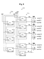
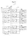
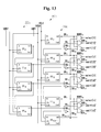
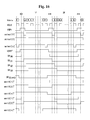
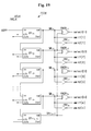
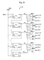
- FIGs. 8, 11, 13, 15, 17, 19, 21, 23, 24, 26 and 27 respectively show scan drivers in organic light emitting diode display devices according to fifth to fifteenth exemplary embodiments
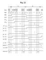
- FIGs. 9, 12, 14, 16, 18, 20, 22, 25, 28 respectively show signal timing diagrams in the scan drivers of FIGs. 8, 11, 13, 15, 17, 19, 21, 24, 26;
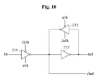
- FIG. 10 shows a flip-flop used in a select scan driver of FIG. 8
- FIG. 29 shows a plan view of an organic light emitting diode display device according to a sixteenth exemplary embodiment of the present invention.
- FIGs. 30A and 30B respectively show odd row and even row scan drivers in the organic light emitting diode display device according to the sixteenth exemplary embodiment.
- FIG. 31 shows a signal timing diagram of the odd row scan driver of FIG. 30A.
- a display device and a driving method thereof according to exemplary embodiments of the present invention will be described in detail with reference to the drawings, and an organic light emitting diode display device using an organic light emitting diode as a light emitting element will be exemplified and described in the exemplary embodiments.
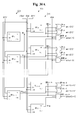
- FIG. 1 shows a plan view of an organic light emitting diode display device according to a first exemplary embodiment of the present invention.
- the organic light emitting diode display device includes a display area 100 seen as a screen to a user, a scan driver 200, and a data driver 300.
- the display area 100 includes a plurality of data lines D 1 to D m , a plurality of select scan lines S 1 to S n , a plurality of emit scan lines Em 11 to Em 1n and Em 21 to Em 2n , and a plurality of unit pixels 110.
- Each unit pixel 110 includes two sub-pixels 111 and 112 which are arranged in a column direction.
- the data lines D 1 to D m are extended in a column direction and transmit data signals representing images to the corresponding unit pixels.
- the select scan lines S 1 to S n are extended in a row direction and transmit select signals for selecting corresponding lines to the select scan lines S 1 to S n in order to apply data signals to the unit pixels of the corresponding lines.
- the emit scan lines Em 11 to Em 1n and Em 21 to Em 2n are extended in a row direction and transmit emission control signals for controlling light emission of the respective sub-pixels 111 or 112 to the corresponding unit pixels 110.
- the unit pixel 110 is defined in an area where the select scan lines S 1 to S n and the data lines D 1 to D m are crossed.
- the scan lines S 1 to S n are coupled to the sub-pixels 111 and 112 in the respective unit pixels 110.
- the scan driver 200 sequentially transmits select signals to the select scan lines S 1 to S n in the respective subfields.
- the scan driver 200 sequentially transmits emission control signals for controlling light emission of the sub-pixels 111 to the emit scan lines Em 11 to Em 1n in one subfield, and sequentially transmits emission control signals for controlling light emission of the sub-pixels 112 to the emit scan lines Em 21 to Em 2n in the other subfield.
- the data driver 300 applies data signals corresponding to the pixels of lines to which select signals are applied to the data lines D 1 to D m each time the select signals are sequentially applied.
- the data driver 300 applies data signals corresponding to the sub-pixels 111 in the one subfield, and applies data signals corresponding to the sub-pixels 112 in the other subfield.
- the scan driver 200 and the data driver 300 are coupled to a substrate in which the display area 100 is formed.
- the scan driver 200 and/or the data driver 300 may be installed directly on the substrate, and they may be substituted with a driving circuit which is formed on the same layer on the substrate as the layer on which scan lines, data lines, and transistors are formed.
- the scan driver 200 and/or the data driver 300 may be installed in a chip format on a tape carrier package (TCP), a flexible printed circuit (FPC), or a tape automatic bonding unit (TAB) coupled to the substrate.
- TCP tape carrier package
- FPC flexible printed circuit
- TAB tape automatic bonding unit
- FIG. 2 shows a simplified circuit diagram of the unit pixels of the organic light emitting diode display device shown in FIG. 1.
- the three unit pixels 110 ij , 110 i(j+1) , and 110 i(j+2) coupled to the scan line S i of the i th row (where 'i' is a positive integer less than or equal to 'n') and the data lines D j to D j+2 of the j th to (j+2) th columns (where 'j' is a positive integer less than or equal to 'm-2') will be exemplified in FIG. 2. It is assumed that the sub-pixels are arranged in an order of R, G, and B along the row direction, and the same color sub-pixels are arranged along the column direction in FIG. 2.
- the two sub-pixels 111 and 112 of the one unit pixel 100 are coupled to one of the select scan lines S 1 to S n in common and have a pixel driver 115 in common, and the pixel driver 115 includes a driving transistor M1, a switching transistor M2, and a capacitor C1.
- the unit pixel 110 ij coupled to the i th select scan line S i and the j th data line D j includes the pixel driver 115, a switching unit, and two organic light emitting diodes OLEO R1 and OLED R2 that emit red light.
- the switching unit includes two emission control transistors M3a and M3b to selectively transmit a driving current from the pixel driver 115 to the two organic light emitting diodes OLED R1 and OLED R2 .
- the sub-pixels 111 ij and 112 ij respectively include the two organic light emitting diodes OLED R1 and OLED R2 in the unit pixel 110 ij .
- the unit pixel 110 i(j+1) coupled to the i th select scan line S i and the (j+1) th data line D j+1 , and the unit pixel 110 i(j+2) coupled to the i th select scan line S i and the (j+2) th data line D j+2 have the same structures as the unit pixel 110 ij .
- sub-pixels 111 i(j+1) and 112 i(j+1) respectively include two organic light emitting diodes OLED G1 and OLED G2 that emit green light in the unit pixel 110 i(j+1)
- sub-pixels 111 i(j+2) and 112 i(j+2) respectively include two organic light emitting diodes OLED B1 and OLED B2 that emit blue light in the unit pixel 110 i(j+2) .
- the driving transistor M1 has a source coupled to a power line for supplying a power supply voltage VDD, and a gate coupled to a drain of the switching transistor M2.
- the capacitor C1 is coupled between the source and the gate of the driving transistor M1.
- the switching transistor M2 having a gate coupled to the select scan line S i and a source coupled to the data line D j , transmits (or applies) the data signal converted to analog voltage (hereinafter, "data voltage”) provided by the data line D j in response to the select signal provided by the select scan line S i .
- the driving transistor M1 has a drain coupled to sources of the emission control transistors M3a and M3b, and gates of the emission control transistors M3a and M3b are coupled to the emit scan lines Em 1i and Em 2i , respectively. Drains of the emission control transistors M3a and M3b are coupled, respectively, to anodes of the organic light emitting diodes OLED R1 and OLED R2 , and a power supply voltage VSS is applied to cathodes of the organic light emitting diodes OLED R1 and OLED R2 .
- the power supply voltage VSS in the first exemplary embodiment is lower than the voltage VDD, and can be a negative voltage or a ground voltage. As shown in FIG. 2, the unit pixels 110 i(j+1) and 110 i(j+2) have the same connecting structure as the unit pixel 110 ij .
- the one emit scan line Em 1i of the emit scan lines Em 1i and Em 2i is coupled to the gates of the transistors M3a respectively coupled to the organic light emitting diodes OLED R1 , OLED G1 and OLED B1
- the other emit scan line Em 2i is coupled to the gates of the transistors M3b respectively coupled to the organic light emitting diodes OLED R2 , OLED G2 and OLED B2 .
- a low-level emission control signal is applied to the emit scan line Em 1i in one subfield of two subfields forming a field, and therefore, the transistor M3a is turned on. Then, a current I OLED as expressed in Equation 1 flows from the transistor M1 to the organic light emitting diode so that the organic light emitting diodes OLED R1 , OLED G1 and OLED B1 emit light corresponding to the magnitude of the current I OLED .
- a low-level emission control signal is applied to the emit scan line Em 2i in the other subfield, and therefore, the transistor M3b is turned on. Then, a current I OLED flows from the transistor M1 to the organic light emitting diode so that the organic light emitting diodes OLED R2 , OLED G2 and OLED B2 emit light.
- I OLED ⁇ 2 (
- ⁇ is a constant determined by a channel width and a channel length of the transistor M1
- V SG is a voltage between the source and the gate of the transistor M1
- V TH is a threshold voltage of the transistor M1.
- an upper line L1 is formed by the organic light emitting diodes OLED R1 , OLED G1 and OLED B1
- a lower line L2 is formed by the organic light emitting diodes OLED R2 , OLED G2 and OLED B2 .
- the organic light emitting diodes of the upper line L1 start emitting light in one subfield of the fields, and the organic light emitting diodes of the lower line L2 start emitting light in the other subfield of the fields.
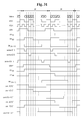
- FIG. 3 A driving method of the organic light emitting diode display device according to the first exemplary embodiment of the present invention will be described in detail with reference to FIG. 3.
- the select signal applied to the select scan line S i is depicted as 'select[i]'
- the emission control signals applied to the emit scan lines Em 1i and Em 2i are depicted as 'emit1[i]' and 'emit2[i]', respectively.
- one field includes two subfields 1 F and 2F, and low-level select signals are sequentially applied to the select scan lines S 1 to S n in each subfield 1 F or 2F.
- the two organic light emitting diodes of the unit pixel that share the select scan line emit light during periods corresponding to subfields 1 F and 2F, respectively.
- widths of low-level signals (e.g., pulses) of the emission control signals emit1[i] and emit2[i] are the same as periods corresponding to the subfields 1 F and 2F, respectively.
- the first subfield 1 F when a low-level select signal select[1] is applied to the select scan line S 1 on the first row, data voltages corresponding to the organic light emitting diodes OLED R1 , OLED G1 , and OLED B1 of the unit pixels on the first row are applied to the corresponding data lines D 1 -D m .
- a low-level emission control signal emit1[1] is applied to the emit scan line Em 11 on the first row, and the emission control transistors M3a of the unit pixels on the first row are turned on.
- a low-level select signal select[2] is applied to the select scan line S 2 on the second row
- data voltages corresponding to the organic light emitting diodes OLED R1 , OLED G1 and OLED B1 of the unit pixels on the second row are applied to the corresponding data lines D 1 -D m .
- a low-level emission control signal emit1[2] is applied to the emit scan line Em 12 on the second row, and the emission control transistors M3a of the unit pixels on the second row are turned on.
- the organic light emitting diodes OLED R1 , OLED G1 and OLED B1 on the upper line L1 of the second row emit light in response to the low-level emission control signal emit1 [2]. The light is emitted during the period in which the emission control signal emit1 [2] is low-level.
- low-level select signals select[1] to select[n] are sequentially applied to the select scan lines S 1 to S n on the first to n th rows in the first subfield 1 F.
- the low-level select signal select[i] is applied to the select scan line S i on the i th row
- the data voltages corresponding to the organic light emitting diodes OLED R1 , OLED G1 and OLED B1 of the unit pixels on the i th row are applied to the corresponding data line D 1 to D m
- a low-level emission control signal emit1[i] is applied to the emit scan line Em 1i of the i th row.
- the organic light emitting diodes OLED R1 , OLED G1 and OLED B1 which are formed on the upper line L1 of the i th row, emit light during a period corresponding to the width of the low-level emission control signal emit1[i].
- a low-level select signal select[1] is applied to the select scan line S 1 on the first row, and data voltages corresponding to the organic light emitting diodes OLED R2 , OLED G2 and OLED B2 of the unit pixels on the first row are applied to the corresponding data lines D 1 -D m .
- a low-level emission control signal emit2[1] is applied to the emit scan line Em 21 on the first row, and the emission control transistors M3b of the unit pixels on the first row are turned on. Then, the organic light emitting diodes OLED R2 , OLED G2 and OLED B2 on the lower line L2 of the first row emit light during the period in which the emission control signal emit2[1] is low-level.
- a low-level select signal select[2] is applied to the select scan line S 2 on the second row, and data voltages corresponding to the organic light emitting diodes OLED R2 , OLED G2 and OLED B2 of the unit pixels on the second row are applied to the corresponding data lines D 1 -D m .
- a low-level emission control signal emit2[2] is applied to the emit scan line Em 22 on the second row, and the emission control transistors M3b of the unit pixels on the second row are turned on. Then, the organic light emitting diodes OLED R2 , OLED G2 and OLED B2 on the lower line L2 of the second row emit light during the period in which the emission control signal emit2[2] is low-level.
- low-level select signals select[1] to select[n] are sequentially applied to the select scan lines S 1 to S n on the first to n th rows in the second subfield 2F.
- the low-level select signal select[i] is applied to the select scan line S i on the i th row
- the data voltages corresponding to the organic light emitting diodes OLED R2 , OLED G2 and OLED B2 of the unit pixels on the i th row are applied to the corresponding data line D 1 to D m
- a low-level emission control signal emit2[i] is applied to the emit scan line Em 2i of the i th row.
- the organic light emitting diodes OLED R2 , OLED G2 and OLED B2 which are formed on the lower line L2 of the i th row, emit light in during a period corresponding to the width of the low-level emission control signal emit2[i].
- one field is divided into the two subfields, and the subfields are sequentially driven in the organic light emitting diode display device driving method according to the first exemplary embodiment.
- the organic light emitting diodes formed on the upper line L1 of the each row start emitting light in one subfield, and the organic light emitting diodes formed on the lower line L2 of the each row start emitting light in the other subfield.
- the organic light emitting diodes of all sub-pixels formed on 2n lines of n rows can emit light in the one field.
- the number of select scan lines and the number of pixel drivers e.g., the transistors and the capacitors
- the number of integrated circuits for driving the select scan lines can be reduced, and the elements can be easily arranged in the unit pixel.
- the scan driver and the data driver of the interlace scan method may be applicable to those according to the first exemplary embodiment of the present invention because the lower lines L2 are scanned after the upper lines L1 are scanned in the first exemplary embodiment.
- the single scan method is applicable to the organic light emitting diode display device in FIG. 3, but the dual scan method may also be applicable to the organic light emitting diode display device according to the first exemplary embodiment by using two scan drivers.
- another scan method, in which the select scan signals are selectively applied to the plurality of select scan lines may also be applicable to the organic light emitting diode display device according to the first exemplary embodiment.
- one sub-pixel 111 ij (including the organic light emitting diode OLED R1 ) of the unit pixel 110 ij is arranged on the upper side of the select scan line S i
- the other sub-pixel 112 ij (including the organic light emitting diode OLED R2 ) of the unit pixel 110 ij is arranged on the lower side of the select scan line S i
- the two sub-pixels 111 ij and 112 ij may be arranged on the lower side (or the upper side) of the select scan line S i .
- FIG. 4 shows a simplified circuit diagram of unit pixels 110 ij ', 110 i(j+1) ' and 110 i(j+2) ' of an organic light emitting diode display device according to a second exemplary embodiment of the present invention.
- the organic light emitting diodes OLED R1 , OLED G1 and OLED B1 are arranged below the pixel driver 115 to form the upper line L1', and the organic light emitting diodes OLED R2 , OLED G2 and OLED B2 are arranged below the upper line L1' to form the lower line L2'.
- the organic light emitting diodes are arranged as shown in FIG. 4, length of a wire for transmitting current from the pixel driver 115 to the organic light emitting diode OLED R2 , OLED G2 or OLED B2 is longer than length of a wire for transmitting current from the pixel driver 115 to the organic light emitting diode OLED R1 , OLED G1 or OLED B1 . Then, the brightness of the upper line L1' may be different from the brightness of the lower line L2' by parasitic components present in the wire.
- the transistors M1, M2, M3a, and M3b are depicted as PMOS transistors in FIGs. 2 and 4, but another conductive type of transistors may be applicable to the transistors M1, M2, M3a, and M3b.
- emission control transistors M3a and M3b are respectively controlled by the two emit scan lines Em 1i and Em 2i in the first and second exemplary embodiments, emission control transistors in other embodiments may be controlled by one emit scan line as shown in FIG. 5.
- FIG. 5 shows a simplified circuit diagram of unit pixels 110 ij “, 110 i(j+1) " and 110 i(j+2) " of an organic light emitting diode display device according to a third exemplary embodiment of the present invention.
- the unit pixel 110 ij " according to the third exemplary embodiment has the same structure as that according to the first exemplary embodiment, except for emission control transistors M3a' and M3b' and an emit scan line Em i .
- an emission control transistor M3a' has the opposite conductive type to an emission control transistor M3b', and the emit scan line Em i on i th row is coupled to gates of the two emission control transistors M3a' and M3b'.
- the emission control transistors M3a' respectively coupled to the organic light emitting diodes OLED R1 , OLED G1 and OLED B1 of the upper line L1 are depicted as PMOS transistors
- the emission control transistors M3b' coupled to the organic light emitting diodes OLED R2 , OLED G2 and OLED B2 of the lower line L2 are depicted as NMOS transistors.
- an emission control signal applied to the emit scan line Em i has the same signal timing as the emission control signal emit1[i] shown in FIG. 3.
- emission timings of the organic light emitting diodes OLED R1 , OLED G1 and OLED B1 coupled to the transistors M3a' are the same as those of the first exemplary embodiment.
- emission control signal emit2[i] has an inverted waveform of the emission control signal emit1[i]
- the transistor M3b' has the opposite conductive type to the transistor M3b shown in FIG. 2
- emission timings of the organic light emitting diodes OLED R2 , OLED G2 and OLED B2 coupled to the transistors M3b' are the same as those of the first exemplary embodiment.
- the number of the emit scan lines Em i according to the third exemplary embodiment can be reduced as compared with those according to the first and second exemplary embodiments.
- the two sub-pixels share the select scan line in the first to third exemplary embodiments, but three or more sub-pixels may share the select scan line in other embodiments.
- three emission control transistors are coupled to the three organic light emitting diodes, respectively.
- the three emit scan lines may be respectively coupled to gates of the three emission control transistors, and may respectively transmit (or apply) emission control signals for controlling the three emission control transistors.
- one field may be divided into three subfields, and the three emission control transistors may be respectively turned on in the three subfields. Then, one row may be divided into the three lines, and the three lines may emit light in the three subfields, respectively.
- the sub-pixels having the same color are coupled to the pixel driver 115 in the first to third exemplary embodiment, but the sub-pixels having different colors may be coupled to the pixel driver 115.
- R organic light emitting diode may be coupled to the upper side of the pixel driver 115 in the unit pixel 110 ij shown in FIG. 2
- G organic light emitting diode may be coupled to the lower side of the pixel driver 115.
- the driving voltages which are respectively transmitted from the driving transistors to the R, G, and B organic light emitting diodes are set to the different ranges.
- the ranges of the data voltages which are transmitted through the data lines to the driving transistors may be set to be different in R, G, and B sub-pixels, or the sizes of the driving transistors may be set to be different in the R, G, and B sub-pixels.
- the colors represented in the sub-pixels sharing the pixel driver are different, the data voltages corresponding to the sub-pixels having the different colors are respectively transmitted to the data line in the respective subfields. Then, the data voltage of the data driver is difficult to be optimized because the data voltage range of the data driver is not optimized to the sub-pixels having the same color and is optimized to or made suitable for the sub-pixels having different colors.
- each output of the data driver can be optimized to the data voltage corresponding to each color. Accordingly, the data voltage transmitted to the one data line can be set to the voltage range corresponding to the one color, and the desired brightness can be represented in the respective sub-pixels. As a result, a white balance can be realized in the display area.
- the pixel driver using the switching and driving transistors and the capacitor is described in the first to third exemplary embodiments, but the plurality of sub-pixels may share a pixel driver which uses at least one transistor and/or at least one capacitor in addition to the switching and driving transistors to compensate variation of the threshold voltage of the driving transistor or the voltage drop. That is, since the driving current outputted from the pixel driver generally depends on the threshold voltage of the driving transistor in the unit pixel shown in FIG. 2, the driving currents may be different if the threshold voltages of the driving transistors are different. Then, the brightness between the unit pixels may be different. A unit pixel which can compensate for a variation of the threshold voltage of the driving transistor will be described with reference to FIG. 6.
- FIG. 6 shows a simplified circuit diagram of a unit pixel of an organic light emitting diode display device according to a fourth exemplary embodiment of the present invention.
- the unit pixel coupled to the scan line S i of the i th row and the data line D j will be exemplified in FIG. 6.
- a scan line for transmitting a current select signal will be referred to as a "current select scan line” and a scan line which has transmitted a select signal before the current select signal is transmitted will be referred to as a "previous select scan line.”
- a pixel driver 115' of the unit pixel according to the fourth exemplary embodiment further includes a threshold voltage compensator for compensating a threshold voltage of a driving transistor.
- the threshold voltage compensator includes two transistors M14 and M15, and a capacitor C12.
- transistors M11, M12, M 13a, and M 13b correspond to the transistors M1, M2, M3a, and M3b shown in FIG. 2, respectively, and capacitors C11 and C12 correspond to the capacitor C1 shown in FIG. 2.
- a first electrode of the capacitor C11 is coupled to a power supply voltage VDD
- a second electrode of the capacitor C11 is coupled to a first electrode of the capacitor C12.
- a second electrode of the capacitor C12 is coupled to a gate electrode of the driving transistor M11
- the switching transistor M12 is coupled to the first electrode of the capacitor C12.
- the transistor M14 is coupled between gate and drain electrodes of the transistor M11, and diode-connects the transistor M11 in response to the select signal of the previous select scan line S i-1 .
- the transistor M15 is coupled between the power supply voltage VDD and the first electrode of the capacitor C12, and couples the first electrode of the capacitor C12 to the power supply voltage VDD in response to the select signal of the previous select scan line S i-1 .
- FIG. 7 An operation of the unit pixel 115 ij ' shown in FIG. 6 will be described with reference to FIG. 7.
- a first subfield in which the organic light emitting diodes formed on the upper line L1 are emitted by turn-on of the transistors M13a will be described only. Therefore, the emission control signal, which is applied to the emit scan line Em 2i and is high-level in the first subfield, is not shown in FIG. 7.
- the transistors M14 and M15 are turned on during a period in which the select signal select[i-1] of the previous select scan line S i-1 is low-level, and the emission control signal emit1 [i]" of the emit scan line Em 1i is high-level. Then, the transistor M14 is diode-connected while the transistor M13a and M13b are turned off, and a voltage between the gate and source electrodes of the transistor M11 becomes the threshold voltage Vth of the transistor M11. In addition, since the capacitor C12 is coupled between the gate and source electrodes of the transistor M 11, a voltage at the gate electrode of the transistor M 11, i.e., the second electrode of the capacitor C12, becomes "VDD+Vth" voltage.
- the transistor M12 is turned on and the transistors M14 and M15 are turned off during a period in which the select signal select[i] of the current select scan line S i is low-level, and the emit control signal emit1[i]" is high-level.
- the data voltage Vdata is applied to the first electrode of the capacitor C12 through the switching transistor M12, a voltage at the second electrode of the capacitor C12 is changed by the variation "Vdata-VDD" of the voltage at the first electrode of the capacitor C12. That is, the voltage at the second electrode of the capacitor C12 becomes “Vdata+Vth” voltage, and therefore, the voltage between the gate and source electrodes of the transistor M11 becomes “Vdata+Vth-VDD” voltage.
- the "Vdata+Vth-VDD" voltage is stored in the capacitors C11 and C12.
- Equation 2 I OLED ⁇ 2 ( V D D ⁇ V data ) 2
- a unit pixel which can compensate the threshold voltage of the driving transistor by adding at least one transistor and/or at least one capacitor to the unit pixel of FIG. 2 may be used instead of the unit pixel shown in FIG. 6.
- the low-level period of the emission control signal may be set differently from the period shown in FIG. 3.
- the low-level period of the emission control signal may be set to be shorter than a period corresponding to the subfield. That is, the rising edge of the emission control signal may be set to be later than the rising edge of the select signal, and/or the falling edge of the emission control signal may be set to be faster (or earlier) than the rising edge of the select signal in the next subfield.
- the organic light emitting diode display device using the voltage programming method is described in the first to fourth exemplary embodiments, but the above-described exemplary embodiments can be applicable to the organic light emitting diode display device using the current programming method.
- scan drivers e.g., the scan driver 200 of FIG. 1
- organic light emitting diode display devices e.g., the scan driver 200 of FIG. 1
- FIG. 8 shows a scan driver 200a in an organic light emitting diode display device according to a fifth exemplary embodiment
- FIG. 9 shows a signal timing diagram in the scan driver 200a of FIG. 8
- FIG. 10 shows a flip-flop used in the select scan driver 200a of FIG. 8.
- An inverted signal of a clock VCLK is depicted as /VCLK in FIG. 8, and is not shown in FIG. 9.
- the scan driver 200a includes two shift registers 210a and 220a.
- the shift register 210a includes (n+1) flip-flops FF 11 to FF 1(n+1) and n NAND gates NAND 11 to NAND 1n
- the shift register 220a includes n flip-flops FF 21 to FF 2n and n inverters INV 21 to INV 2n .
- a start signal VSP1 is inputted to the first flip-flop FF 11 , and an output signal SR 1i of the i th flip-flop FF 1i is inputted to the (i+1) th flip-flop FF 1(i+1) .
- the i th NAND gate NAND 1i performs a NAND operation to the output signals SR 1i and SR 1(i+1) of the two adjacent flip-flops FF 1i and FF 1(i+1) and outputs a select signal select[i].
- a start signal VSP2 is inputted to the first flip-flop FF 21 , and an output signal of the i th flip-flop FF 2i is inputted to the (i+1) th flip-flop FF 2(i+1) .
- the output signal of the i th flip-flop FF 2i is the emission control signal emit2[i]
- the inverter INV 2i inverts the output signal of the i th flip-flop FF 2i to output the emission control signal emit1 [i].
- the flip-flops FF 1i and FF 2i output input signals (in) in response to a high-level clock (clk), and latch and output the input signals (in) of the high-level period of the clock (clk) in response to a low-level clock (clk). That is, the flip-flops FF 1i and FF 2i output the input signals (in) of the high-level period of the inner clock (clk) during one clock VCLK cycle.
- the clock /VCLK or VCLK inverted to the clock VCLK or /VCLK, which are used in the flip-flop FF 1i are used in the flip-flops FF 1(i+1) adjacent to the flip-flop FF 1i .
- the flip-flops FF 1i that are located at odd-numbered positions in a longitudinal direction use the clocks VCLK as inner clocks (clk).
- the flip-flops FF 1i that are located at even-numbered positions in the longitudinal direction use the inverted clocks /VCLK as inner clocks (clk).
- the output signal SR 1i of the flip-flop FF 1i is inputted to the flip-flop FF 1(i+1) , the output signal SR 1(i+1) of the flip-flop FF 1(i+1) is shifted from the output signal SR 1i of the flip-flop FF 1i by a half clock VCLK cycle.
- the start signal VSP1 has a high-level signal (e.g., high-level pulse) in the high-level period of the one clock VCLK cycle in each of the subfields 1 F and 2F, and the flip-flop FF 11 outputs the high-level signal during one clock VCLK cycle in each of the subfields 1 F and 2F.
- the flip-flops FF 11 to FF 1(n+1) may sequentially output each output signal SR 1i by shifting the high-level signal by the half clock VCLK cycle.
- the NAND gate NAND 1i performs a NAND operation of the output signals SR 1i and SR 1(i+1) of the flip-flops FF 1i and FF 1(i+1) , and outputs a low-level signal (e.g., low-level pulse) when both output signals SR 1i and SR 1(i+1) are high-level.
- a low-level signal e.g., low-level pulse
- the output signal select[i] of the NAND gate NAND 1i has a low-level signal during a period in which the both output signals SR 1i and SR 1(i+1) have the high-level signal in common in each of the subfields 1 F and 2F.
- the output signal select[i+1] of the NAND gate NAND 1(i+1) is shifted from the output signal select[i] of the NAND gate NAND 1i by half the clock VCLK cycle. Therefore, the shift register 210a may sequentially output each select signal select[i] by shifting the low-level signal by the half clock VCLK cycle.
- the flip-flop FF 2i of the shift register 220a has the same structure as the flip-flop FF 1i of the shift register 210a except for the clocks VCLK and /VCLK. That is, the flip-flops FF 2i that are located at odd-numbered positions in the longitudinal direction use the inverted clocks /VCLK as inner clocks (clk), and the flip-flops FF 2i that are located at the even-numbered positions use the clocks VCLK as inner clocks (clk).
- the emission control signal emit1[i+1] which is the output signal of the flip-flop FF 2(i+1) is shifted from the emission control signal emit1 [i], which is the output signal of the flip-flop FF 2i , by the half clock VCLK cycle.
- the start signal VSP2 is high-level in the low-level period of all clock VCLK cycles in the subfield 1 F and is low-level in the low-level period of all clock VCLK cycles in the subfield 2F.
- the emission control signal emit2[1] becomes high-level when the select signal select[1] becomes low-level in the first subfield 1 F, and becomes low-level when the select signal select[1] becomes low-level in the second subfield 2F. Therefore, the shift register 220a can sequentially output each emission control signal emit2[i], which becomes low-level together with the select signal select[i] in the second subfield 2F, by shifting the half clock VCLK cycle.
- the shift register 220a can sequentially output each emission control signal emit1[i], which becomes low-level together with the select signal select[i] in the first subfield 1 F, by shifting the half clock VCLK cycle.
- the flip-flop (e.g., FF 1i ) includes a clocked inverter 211, and a latch including an inverter 212 and a clocked inverter 213.
- the clocked inverter 211 inverts an input signal (in) when the clock (clk) is high-level, and the inverter 212 inverts the output signal (/out) of the clocked inverter 211.
- the output of the clocked inverter 211 is blocked, the output signal of the inverter 212 is inputted to the clocked inverter 213, and the output signal (/out) of the clocked inverter 213 is inputted to the inverter 212.
- the latch is formed.
- the output signal (out) of the inverter 212 is the output signal of the flip-flop, and the input signal (/out) of the inverter 212 is the inverted signal to the output signal (out).
- the flip-flop can output the input signal (in) when the clock (clk) is high-level, and latch and output the input signal (in) in the high-level period of the clock (clk) when the clock (clk) is low-level.
- the signal (/out) inverted to the output signal (out) is outputted from the flip-flop (e.g., FF 2i ) of the shift register 220a. Therefore, the inverted output signal (/out) of the flip-flop of FIG. 10 may be used as the emission control signal emit1 [i] of the first subfield 1 F, and the inverter INV 2i can be eliminated in the shift register 220a.
- the signal having the high-level signal in the first subfield 1 F is used as the start signal VSP2 in FIGs. 8 and 9, but a signal inverted to the start signal VSP2 may be used as the start signal of the shift register 220a. Then, the output signal of the flip-flop becomes the emission control signal emit1 [i] of the first subfield 1 F, and the output signal of the inverter INV 2i becomes the emission control signal emit2[i] of the second subfield 2F.
- the emission control signal emit1 [i] or emit2[i] is low-level when the select signal select[i] is low-level in the scan driver 200a.
- This signal timing can be applicable to the organic light emitting diode display device using the voltage programming method in which the data voltage is transmitted to the data line to be stored in the capacitor.
- the current from the driving transistor needs to be blocked from the organic light emitting diodes when the data current are programmed to the pixel driver. That is, emission control signals emit1 [i]' and emit2[i]' should be high-level when the select signal select[i] is low-level.
- this signal timing may be applicable to the organic light emitting diode display device using the voltage programming method.
- FIG. 11 shows a scan driver 200b in an organic light emitting diode display device according to a sixth exemplary embodiment
- FIG. 12 shows a signal timing diagram in the scan driver 200b of FIG. 11.
- the scan driver 200b of FIGs. 11 and 12 use the same clock VCLK as the scan driver 200a shown in FIGs. 8 and 9.
- the scan driver 200b includes the shift register 210a for outputting the select signal select[i] and a shift register 220b for outputting the emission control signals emit1[i]' and emit2[i]'.
- the shift register 220b includes (n+1) flip-flops FF 31 to FF 3(n+1) , n NAND gates NAND 31 to NAND 3n , and n OR gates OR 31 to OR 3n .
- a NAND gate and an inverter may be used instead of the OR gate OR 3i .
- the clock VCLK is inputted to the flip-flops FF 3i , and the NAND gate NAND 3i performs a NAND operation between the output signals SR 3i and SR 3(i+1) of the flip-flops FF 3i and FF 3(i+1) to output the emission control signal emit1[i]'.
- the OR gate OR 3i performs an OR operation between the output signals SR 3i and SR 3(i+1) of the flip-flops FF 3i and FF 3(i+1) to output the emission control signal emit2[i]'.
- the start signal VSP2 shown in FIG. 9 is inputted to the flip-flop FF 3i . Therefore, the output signal SR 3i of the flip-flop FF 3i becomes high-level when the select signal select[i] becomes low-level in the first subfield 1F, and becomes low-level when the select signal select[i] becomes low-level in the second subfield 2F. Since the NAND gate NAND 3i outputs the low-level signal while both the output signal SR 3i and SR 3(i+1) of the flip-flops FF 3i and FF 3(i+1) are high-level, the emission control signal emit1[i]' becomes low-level when the select signal select[i] becomes high-level in the first subfield 1 F.
- the OR gate OR 3i outputs the high-level signal while both the output signal SR 3i and SR 3(i+1) of the flip-flops FF 3i and FF 3(i+1) are low-level, the emission control signal emit2[i]' becomes low-level when the select signal select[i] becomes high-level in the second subfield 2F.
- emission control signals emit1 [i]' and emit2[i]' are high-level in the sixth exemplary embodiment when the select signal select[i] has the low-level signal.
- emission control signals emit1 [i]" and emit2[i]" may be high-level when the previous and current select signals select[i-1] and select[i] have the low-level signals. This exemplary embodiment will be described with reference to FIGs. 13 and 14.
- FIG. 13 shows a scan driver 200c in an organic light emitting diode display device according to a seventh exemplary embodiment
- FIG. 14 shows a signal timing diagram of the scan driver 200c shown in FIG. 13.
- the scan driver 200c of FiGs. 13 and 14 use the same clock VCLK as the scan driver 200a shown in FIGs. 8 and 9.
- the scan driver 200c includes the shift register 210a for outputting the select signal select[i] and a shift register 220c for outputting the emission control signals emit1[i]" and emit2[i]".
- the shift register 220c includes n flip-flops FF 41 to FF 4n , n inverters INV 41 to INV 4n , and 2n NOR gates NOR 11 to NOR 1n , and NOR 4 , to NOR 4n .
- the flip-flops FF 41 to FF 4n and the inverters INV 41 to INV 4n have the same structure as the flip-flops FF 21 to FF 2n and the inverters INV 21 to INV 2n of FIG. 8 except for the clocks VCLK and /VCLK. That is, the flip-flop FF 4i uses the clock VCLK or /VCLK inverted to the clock /VCLK or VCLK of the flip-flop FF 2i shown in FIG. 8.
- the NOR gate NOR 1i performs a NOR operation between the output signal SR 1i of the flip-flop FF 1i and the inverted output signal /SR 4i of the flip-flop FF 4i to output the emission control signal emit1[i]" in the first subfield 1 F.
- the NOR gate NOR 4i performs a NOR operation between the output signals SR 1i and SR 4i of the flip-flops FF 1i and FF 4i to output the emission control signal emit2[i]" in the second subfield 2F.
- a start signal VSP2' is high-level in the high-level period of the clock VCLK in the first subfield 1 F and is low-level in the high-level period of the clock VCLK in the second subfield 2F.
- the output signal SR 4i of the flip-flop FF 4i has the high-level signal during a period corresponding to the first subfield 1 F and has the low-level signal during a period corresponding to the second subfield 2F.
- the output signal SR 4i of the flip-flop FF 4i becomes high-level when the output signal SR 1i of the flip-flop FF 1i becomes high-level in the first subfield 1 F, and becomes low-level when the output signal SR 1i of the flip-flop FF 1i becomes high-level in the second subfield 2F.
- the output signal emit1[i]" of the NOR gate NOR 1i becomes low-level together with the output signal SR 1i in the first subfield 1 F and becomes high-level together with the output signal SR 1i in the second subfield 2F.
- the output signal emit2[i]" of the NOR gate NOR 4i becomes low-level together with the output signal SR 1i in the second subfield 2F and becomes high-level together with the output signal SR 1i in the first subfield 1 F. Therefore, the emission control signals emit1 [i]" and emit2[i]" are high-level when the previous and current select signals select[i-1] and select[i] have the low-level signals.
- emission control signals emit1 [i]" and emit2[i]" shown in FIG. 14 may be generated from the scan driver shown in FIG. 11. This exemplary embodiment will be described with reference to FIGs. 15 and 16.
- FIG. 15 shows a scan driver 200d in an organic light emitting diode display device according to an eight exemplary embodiment
- FIG. 16 shows a signal timing diagram of the scan driver 200d shown in FIG. 15.
- the scan driver 200d includes the shift register 210a for outputting the select signal select[i] and a shift register 220d for outputting the emission control signals emit1 [i]" and emit2[i]".
- the shift register 220d further includes a flip-flop FF 30 before the flip-flop FF 31 , which is different from the shift register 220b of FIG. 11, and a start signal VSP2" is inputted to the flip-flop FF 30 .
- the flip-flop FF 30 receives the clock VCLK as the inner clock (clk).
- the i th NAND gate NAND 3i performs a NAND operation between the output signals SR 3(i-1) and SR 3(i+1) of the (i-1) th and (i+1) th flip-flops FF 3(i-1) and FF 3(i+1) to output the emission control signal emit1 [i]".
- the i th OR gate OR 3i performs an OR operation between the output signals SR 3(i-1) and SR 3(i+1) of the (i-1) th and (i+1) th flip-flops FF 3(i-1) and FF 3(i+1) to output the emission control signal emit2[i]".
- the start signal VSP2" is high-level when the clock VCLK is high-level in the first subfield 1 F, and is low-level when the clock VCLK is high-level in the second subfield 2F. Then, the output signal SR 3i of the flip-flop FF 3i is same as that SR 3i shown in FIG. 12. Therefore, the emission control signals emit1[i]” and emit2[i]" are high-level when the previous and current select signal select[i-1] and select[i] have the low-level signals.
- the select signals and the emission control signals are generated from the two shift registers each including the plurality of flip-flops.
- exemplary embodiment which may reduce the number of the flip-flops compared to these exemplary embodiments, will be described.
- FIG. 17 shows a scan driver 200e in an organic light emitting diode display device according to a ninth exemplary embodiment
- FIG. 18 shows a signal timing diagram of the scan driver 200e shown in FIG. 17.
- a clock VCLK' used in the scan driver 200e of FIGs. 17 and 18 has twice the period of the clock VCLK of FIGs. 8 to 16, and the inverted clock /VCLK' is not shown in FIG. 18.
- the scan driver 200e includes a shift register 210e for outputting the select signal select[i] and a shift register 220e for outputting the emission control signals emit1[i]" and emit2[i]".
- the shift register 210e includes ((n/2)+1) flip-flops FF 51 to FF s(n/2+1) , n NAND gates NAND 51 to NAND 5(n/2) , and NAND 61 to NAND 6(n/2)
- the shift register 220e includes (n/2) flip-flops FF 61 to FF 6(n/2) , and n OR gates OR 51 to OR 5(n/2) , and OR 61 to OR 6(n/2) (where 'n' is assumed to an even number).
- the clocks VCLK' and /VCLK' of the flip-flop FF 5(j+1) are inverted to the clocks /VCLK' and VCLK' of the adjacent flip-flops FF 5j in the shift register 210e (where 'j' is a positive integer less than or equal to 'n/2'), and the clock VCLK' is inputted to the flip-flop FF 51 as the inner clock (clk). As shown in FIG.
- the flip-flops FF 51 to FF 5(n/2+1) may sequentially output each output signal SR 5i by shifting the high-level signal by the half clock VCLK' cycle.
- the output signal SR 5i has the high-level signal during one clock VCLK' cycle in each of the subfields 1 F and 2F.
- the j th NAND gate NAND 5j performs a NAND operation of the output signals SR 5j and SR 5(j+1) of the flip-flops FF 5j and FF 5(j+1) , and the inverted clock /VCLK to output the (2j-1) th select signal select[2j-1]. Therefore, the select signal select[2j-1] has the low-level signal during a low-level period of the clock VCLK of a period in which the both output signals SR 5j and SR 5(j+1) are high-level.
- the j th NAND gate NAND 6j performs the NAND operation of the output signals SR 5j and SR 5(j+1) of the flip-flops FF 5j and FF 5(j+1) , and the clock VCLK to output the (2j) th select signal select[2j]. Therefore, the select signal select[2j] has the low-level signal during a high-level period of the clock VCLK of the period in which the both output signals SR 5j and SR 5(j+1) are high-level.
- the clocks VCLK' and /VCLK' of the flip-flop FF 6(j+1) are inverted to the clocks /VCLK' and VCLK' of the adjacent flip-flops FF 6j in the shift register 212e, and the inverted clock /VCLK' is inputted to the flip-flop FF 61 as the inner clock (clk).
- the flip-flops FF 61 to FF 6(n/2) may sequentially output each output signal SR 6i by shifting the high-level signal by the half clock VCLK' cycle.
- the output signal SR 6i has the high-level signal during a period corresponding to the first subfield 1 F.
- the j th OR gate OR 5j performs an OR operation of the output signal SR 5j of the flip-flop FF 5j and the inverted output signal /SR 6j of the flip-flop FF 6j to output the (2j-1) th and (2j) th emission control signals emit1 [2j-1]” and emit1[2j]” (shown as emit1 [2j-1, 2j] in FIG. 17) in the first subfield 1F. Therefore, the emission control signals emit1[2j-1]" and emit1[2j]” have the low-level signal during a period in which the both output signal SR 5j of the flip-flop FF 5j and inverted output signal /SR 6j of the flip-flop FF 6j are low-level.
- the j th OR gate OR 6j performs the OR operation of the output signal SR 5j of the flip-flop FF 5j and the output signal SR 6j of the flip-flop FF 6j to output the (2j-1) th and (2j) th emission control signals emit2[2j-1]" and emit2[2j]” (shown as emit2[2j-1, 2j] in FIG. 17) in the second subfield 2F. Therefore, the emission control signals emit2[2j-1]" and emit2[2j]” have the low-level signal during a period in which the both output signals SR 5j and SR 6j of the flip-flops FF 5j and FF 6j are low-level.
- the emission control signals emit1[2j-1]" and emit2[2j-1]" are high-level when the previous and current select signals select[2j-2] and select[2j-1] have the low-level signals, and the emission control signals emit1[2j]" and emit2[2j]" are high-level when the previous and current select signals select[2j-1] and select[2j] have the low-level signal.
- a scan driver 200f for outputting the emission control signals emit1[i] and emit2[i] shown in FIG. 9 will be described with reference to FIGs. 19 and 20.
- FIG. 19 shows the scan driver 200f in an organic light emitting diode display device according to a tenth exemplary embodiment
- FIG. 20 shows a signal timing diagram of the scan driver 200f shown in FIG. 19.
- the scan driver 200f includes (n+1) flip-flops FF 71 to FF 7(n-1) , n XNOR gates XNOR 71 to XNOR 7n , and n inverters INV 71 to INV 7n , and operates as a shift register.
- the flip-flops FF 71 to FF 7(n+1) and the n inverters INV 71 to INV 7n have the same structure as the flip-flops FF 11 to FF 1(n+1) and the n inverters INV 21 to INV 2n shown in FIG. 8.
- the flip-flops FF 71 to FF 7(n+1) use the clock VCLK and the start signal VSP2 shown in FIG. 9.
- an output signal SR 7i of the flip-flop FF 7i is same as the emission control signal emit1[i] of the first subfield 1 F, and the output signal of the inverter INV 7i is same as the emission control signal emit2[i] of the second subfield 2F.
- the inverted output signal (/out) of the flip-flop FF 7i may be used as the emission control signal emit2[i] instead of the output signal of the inverter INV 7i .
- the XNOR gate XNOR 7i performs XNOR operation between the output signals SR 7i and SR 7(i+1) of the flip-flops FF 7i and FF 7(i+1) to output the select signal select[i]. That is, the XNOR gate XNOR 7i outputs the low-level select signal select[i] while the output signals SR 7i and SR 7(i+1) of the flip-flops FF 7i and FF 7(i+1) have the different levels.
- the select signal select[i] has the low-level signals during a period corresponding to the half clock VCLK cycle from the falling edge of the output signal SR 7i and a period corresponding to the half clock VCLK cycle from the rising edge of the output signal SR 7i .
- the emission control signals emit1[i] and emit2[i] become low-level together with the select signal select[i] in the first and second subfields 1 F and 2F, respectively.
- scan drivers 200g and 220h for outputting the emission control signals emitl[i]' and emit2[i]' shown in FIG. 12 will be described with reference to FIGs. 21 to 23.
- FIG. 21 shows the scan driver 200g in an organic light emitting diode display device according to an eleventh exemplary embodiment
- FIG. 22 shows a signal timing diagram of the scan driver 200g shown in FIG. 21.
- the scan driver 200g has the same structure as the scan driver 200f of FIG. 19 except that the emission control signals emit1 [i]' and emit2[i]' are generated from a NAND gate NAND 7i and an OR gate OR 7i .
- the i th NAND gate NAND 7i performs a NAND operation between the output signals SR 7i and SR 7(i+1) of the flip-flops FF 7i and FF 7(i+1) to output the emission control signal emit1 [i]' of the first subfield 1 F
- the i th OR gate OR 7i performs an OR operation between the output signals SR 7i and SR 7(i+1) of the flip-flops FF 7i and FF 7(i+1) to output the emission control signal emit2[i]' of the second subfield 2F.
- the emission control signals emit1[i]' and emit2[i]' are at high-level in a period corresponding to the low-level signal of the select signal select[i]
- the emission control signals emit1[i]' and emit2[i]' shown in FIG. 22 can be outputted.
- FIG. 23 shows the scan driver 200h in an organic light emitting diode display device according to a twelfth exemplary embodiment.
- the scan driver 200h has the same structure as the scan driver 200g of FIG. 21 except that the select signal select[i] are generated from a NAND gate NAND 8i .
- the two emission control signal emit1[i]' and emit2[i]' have high-levels during a period in which the select signal select[i] has low-level. Therefore, the select signal select[i] can be generated by the NAND operation of the emission control signals emit1[i]' and emit2[i]' which is performed by the NAND gate NAND 8i .
- FIG. 24 shows the scan driver 200i in an organic light emitting diode display device according to a thirteenth exemplary embodiment
- FIG. 25 shows a signal timing diagram of the scan driver 200i shown in FIG. 24.
- the scan driver 200i of FIG. 24 further includes 2n OR gates OR 11 to OR 1n and OR 21 , to OR 2n in addition to the elements of the scan driver 200g of FIG. 21, and the flip-flops FF 71 to FF 7n are not shown in FIG. 24.
- the i th OR gates OR 1i and OR 2i (i-1) th and i th NAND gates NAND 7(i-1) and NAND 7i , (i-1) th and i th OR gates OR 7(i-1) and OR 7i , and i th XNOR gate XNOR 7i are shown in FIG. 24. In FIGs.
- the signals SR 7(i-1) , SR 7i , and SR 7(i+1) respectively correspond to the output signals of the flip-flops FF 7(i-1) , FF 7i , and FF 7(i+1)
- signals A i and B i respectively correspond to the emission control signals emit1[i]' and emit2[i]' of the scan driver 200g shown in FIG. 21.
- the OR gate OR 1i performs an OR operation of the signals A i-1 and A i to output the emission control signals emit1[i]" during a period in which the both signals A i-1 and A i are low-level.
- the OR gate OR 2i performs an OR operation of the signals B i-1 and B i to output the emission control signals emit2[i]" during a period in which the both signals B i-1 and B i are low-level.
- These emission control signals emit1[i]" and emit2[i]" are same as those shown in FIG. 14.
- the low-level periods of the emission control signals emit1 [i]" and emit2[i]" may be controlled by an integral multiple of the half clock VCLK cycle.
- FIG. 26 shows a scan driver 200j in an organic light emitting diode display device according to a fourteenth exemplary embodiment.
- the scan driver 200j includes a NAND gate NAND 8i instead of the XNOR gate XNOR 7i in the scan driver 200i of FIG. 24.
- the i th NAND gate NAND 8i performs a NAND operation of the output signal A i of the i th NAND gate NAND 7i and the output signal B i of the i th OR gate OR 7i to output the select signal select[i] as described in reference to FIG. 23.
- the width of the low-level signal of the select signal select[i] is same as the half clock VCLK cycle. That is, the rising edge of the select signal select[i-1] corresponds to the falling edge of the select signal select[i]. In other embodiment, however, the falling edge of the select signal select[i] may be apart from the rising edge of the select signal select[i-1]. That is, the width of the low-level signal of the select signal select[i] may be shorter than the half clock VCLK cycle.
- FIGs. 27 and 28 will be described with reference to FIGs. 27 and 28.
- FIG. 27 shows a scan driver 200k in an organic light emitting diode display device according to a fifteenth exemplary embodiment
- FIG. 28 shows a signal timing diagram of the scan driver 200k shown in FIG. 27.
- the low-level signal width e.g., low-level pulse width
- the scan driver 200k has the same structure as the scan driver 200a of FIGs. 8 and 9 except for a clip signal CLIP, and NAND gates NAND 11i (i.e., NAND 111 to NAND 11n ), to which the clip signal CLIP is applied in addition to the output signals SR 1i and SR 1(i+1) .
- the clip signal CLIP has a cycle corresponding to the half clock VCLK cycle, and has the low-level signal whose width is shorter than the half clock VCLK cycle.
- the low-level period of the clip signal CLIP includes the falling edge or the rising edge of the clock VCLK.
- the NAND gate NAND 11i outputs the low-level signal of the select signal select[i]' (i.e., one of select signals select[1]' to select[n]') during a period in which the clip signal CLIP is high-level. That is, the falling edge of the select signal select[i]' is apart from the rising edge of the select signal select[i-1]' by the low-level signal width (e.g., low-level pulse width) of the clip signal CLIP.
- the low-level signal width e.g., low-level pulse width
- the scan driver may be divided into a scan driver for driving the unit pixels formed on the odd row (hereinafter, “an odd row scan driver”) and a scan driver for driving the unit pixels formed on the even row (hereinafter, “an even row scan driver”).
- an odd row scan driver for driving the unit pixels formed on the odd row
- an even row scan driver for driving the unit pixels formed on the even row
- FIG. 29 shows a plan view of an organic light emitting diode display device according to a sixteenth exemplary embodiment of the present invention
- FIGs. 30A and 30B respectively show odd row and even row scan drivers 201 and 202 in the organic light emitting diode display device according to the sixteenth exemplary embodiment
- FIG. 31 shows a signal timing diagram of the odd row scan driver 201 shown in FIG. 30A.
- the organic light emitting diode display device As shown in FIG. 29, the organic light emitting diode display device according to the sixteenth exemplary embodiment has the same structure as that of FIG. 1 except for the scan drivers 201 and 202.
- the odd row scan driver 201 is formed on one side of the display area 100, and sequentially transmits the select signals select[2j-1] to the odd-numbered select scan lines S 2j-1 (where 'j' is a positive integer less than or equal to n/2).
- the even row scan driver 202 is formed on the other side of the display area 100, and sequentially transmits the select signals select[2j] to the even-numbered select scan lines S 2j .
- the odd row scan driver 201 sequentially transmits emission control signals emit1[2j-1]" to the odd-numbered emit scan lines Em 1(2j-1) in the first subfield 1 F, and sequentially transmits emission control signals emit2[2j-1]" to the odd-numbered emit scan lines Em 2(2j-1) in the second subfield 2F.
- the even row scan driver 202 sequentially transmits emission control signals emit1 [2j]" to the even-numbered emit scan lines Em 1(2j) in the first subfield 1 F, and sequentially transmits emission control signals emit2[2j]” to the even-numbered emit scan lines Em 2(2j) in the second subfield 2F.
- the odd row scan driver 201 has a structure in which NAND gates NAND 61 to NAND 6(n/2) for even-numbered select signals are eliminated from the scan driver 200e shown in FIG. 17.
- the odd row scan driver 201 includes a shift register 211 for outputting the odd-numbered select signals select[2j-1] and a shift register 221 for outputting the odd-numbered emission control signals emit1[2j-1]" and emit2[2j-1]".
- the shift register 211 includes ((n/2)+1) flip-flops FF 81 , FF 83 , ..., FF 8(n+1) , and (n/2) NAND gates NAND 91 , NAND 93 , ..., NAND 9(n-1)
- the shift register 221 includes (n/2) flip-flops FF 91 , FF 93 , ..., FF 9(n-1) , and n OR gates OR 81 , OR 83 , ..., OR 8(n-1) , and OR 91 , OR 93 , ..., OR 9(n-1) .
- the even row scan driver 202 has a structure in which the NAND gates NAND 51 to NAND 5(n/2) for odd-numbered select signals are eliminated from the scan driver 200e shown in FIG. 17.
- the even row scan driver 202 includes a shift register 212 for outputting the even-numbered select signal select[2j] and a shift register 222 for outputting the even-numbered emission control signals emit1[2j]" and emit2[2j]".
- the shift register 212 includes ((n/2)+1) flip-flops FF 82 , FF 84 , ..., FF 8(n+2) , and (n/2) NAND gates NAND 92 , NAND 94 , ..., NAND 9n , and the shift register 212 includes (n/2) flip-flops FF 92 , FF 94 , ..., FF 9n , and n OR gates OR 82 , OR 84 , ..., OR 8n , and OR 92 , OR 94 , ..., OR 9n .
- the start signal VSP1' shown in FIG. 18 is inputted to the flip-flops FF 81 , and FF 82
- the start signal VSP2" shown in FIG. 18 is inputted to the flip-flops FF 91 and FF 92 .
- the NAND gate NAND 9(2j-1) of the scan driver 201 performs a NAND operation of the output signals SR 8(2j-1) and SR 8(2j+1) of the flip-flops FF 8(2j-1) and FF 8(2j+1) and the clock VCLK to output the (2j-1) th select signal select[2j-1].
- the NAND gate NAND 9(2j) of the scan driver 202 performs a NAND operation of the output signals SR 8(2j) and SR 8(2j+2) of the flip-flops FF 8(2j) and FF 8(2j+2) and the inverted clock /VCLK to output the (2j) th select signal select[2j].
- the OR gate OR 8(2j-1) performs an OR operation of the output signal SR 8(2j-1) of the flip-flop FF 8(2j-1) and the inverted output signal /SR 9(2j-1) of the flip-flop FF 9(2j-1) to output the (2j-1) th emission control signal emit1[2j-1]
- the OR gate OR 9(2j-1) performs an OR operation of the output signals SR 8(2j-1) and SR 9(2j-1) of the flip-flops FF 8(2j-1) and FF 9(2j-1) to output the (2j-1) th emission control signal emit2[2j-1]".
- the OR gate OR 8(2j) performs an OR operation of the output signal SR 8(2j) of the flip-flop FF 8(2j) and the inverted output signal /SR 9(2j) of the flip-flop FF 9(2j) to output the (2j) th emission control signal emit1[2j]
- the OR gate OR 9(2j) performs an OR operation of the output signals SR 8(2j) and SR 9(2j) of the flip-flops FF 8(2j) and FF 9(2j) to output the (2j) th emission control signal emit2[2j]".
- one or more buffers may be formed between the display area 100 and the scan driver 200 (or the scan drivers 201 and 202).
- one or more level shifters which change the levels of the select signals and the emission control signals may also be formed between the display area 100 and the scan driver 200 (or the scan drivers 201 and 202).
- the plurality of sub-pixels share the select scan line and the pixel driver in the unit pixel.
- the sub-pixels can be easily arranged in the unit pixel, and the aperture ratio of the unit pixel can be improved.
- the number of the select scan lines is reduced compared to that of the number of the row lines, the number of the output terminals and the dimension of the scan driver can be reduced. Further, since the dimension of the scan driver is reduced, the non-emission area can be reduced when the scan driver and the unit pixels are formed on the same substrate.
- the number of the flip-flops can be reduced in the scan driver for outputting the select signals and the emission control signals of the first and second subfields.
Landscapes
- Engineering & Computer Science (AREA)
- Theoretical Computer Science (AREA)
- General Physics & Mathematics (AREA)
- Computer Hardware Design (AREA)
- Physics & Mathematics (AREA)
- Environmental Sciences (AREA)
- Life Sciences & Earth Sciences (AREA)
- Biodiversity & Conservation Biology (AREA)
- Animal Husbandry (AREA)
- Control Of Indicators Other Than Cathode Ray Tubes (AREA)
- Control Of El Displays (AREA)
- Electroluminescent Light Sources (AREA)
- Shift Register Type Memory (AREA)
Applications Claiming Priority (1)
| Application Number | Priority Date | Filing Date | Title |
|---|---|---|---|
| KR1020050000759A KR100599657B1 (ko) | 2005-01-05 | 2005-01-05 | 표시 장치 및 그 구동 방법 |
Publications (3)
| Publication Number | Publication Date |
|---|---|
| EP1679687A2 true EP1679687A2 (fr) | 2006-07-12 |
| EP1679687A3 EP1679687A3 (fr) | 2007-03-14 |
| EP1679687B1 EP1679687B1 (fr) | 2012-06-13 |
Family
ID=36118291
Family Applications (1)
| Application Number | Title | Priority Date | Filing Date |
|---|---|---|---|
| EP06100105A Expired - Lifetime EP1679687B1 (fr) | 2005-01-05 | 2006-01-05 | Dispositif d'affichage et son procédé de commande |
Country Status (5)
| Country | Link |
|---|---|
| US (3) | US7847765B2 (fr) |
| EP (1) | EP1679687B1 (fr) |
| JP (1) | JP2006189756A (fr) |
| KR (1) | KR100599657B1 (fr) |
| CN (1) | CN100428317C (fr) |
Cited By (5)
| Publication number | Priority date | Publication date | Assignee | Title |
|---|---|---|---|---|
| US20120313903A1 (en) * | 2011-06-10 | 2012-12-13 | Samsung Mobile Display Co., Ltd. | Organic light emitting display |
| US9129555B2 (en) | 2012-12-20 | 2015-09-08 | Lg Display Co., Ltd. | Light emitting diode display device |
| US10510294B2 (en) | 2016-10-28 | 2019-12-17 | Boe Technology Group Co., Ltd. | Pixel driving circuit, method for driving the same and display device |
| US10803789B1 (en) | 2019-06-12 | 2020-10-13 | Innolux Corporation | Light-emitting device |
| EP3825993A1 (fr) * | 2019-11-21 | 2021-05-26 | Beijing Xiaomi Mobile Software Co., Ltd. | Panneau d'affichage et dispositif électronique |
Families Citing this family (121)
| Publication number | Priority date | Publication date | Assignee | Title |
|---|---|---|---|---|
| KR100578841B1 (ko) * | 2004-05-21 | 2006-05-11 | 삼성에스디아이 주식회사 | 발광 표시 장치와, 그 표시 패널 및 구동 방법 |
| CA2490858A1 (fr) | 2004-12-07 | 2006-06-07 | Ignis Innovation Inc. | Methode d'attaque pour la programmation a tension compensee d'affichages del organiques a matrice active |
| KR100599657B1 (ko) * | 2005-01-05 | 2006-07-12 | 삼성에스디아이 주식회사 | 표시 장치 및 그 구동 방법 |
| CN102663977B (zh) | 2005-06-08 | 2015-11-18 | 伊格尼斯创新有限公司 | 用于驱动发光器件显示器的方法和系统 |
| KR100624114B1 (ko) | 2005-08-01 | 2006-09-15 | 삼성에스디아이 주식회사 | 유기전계발광장치의 주사구동장치 |
| KR100658284B1 (ko) * | 2005-09-30 | 2006-12-14 | 삼성에스디아이 주식회사 | 주사 구동회로와 이를 이용한 유기 전계발광 장치 |
| KR101167663B1 (ko) * | 2005-10-18 | 2012-07-23 | 삼성전자주식회사 | 게이트 구동 회로 및 이를 포함하는 액정 표시 장치 |
| US7916112B2 (en) * | 2005-10-19 | 2011-03-29 | Tpo Displays Corp. | Systems for controlling pixels |
| US9269322B2 (en) | 2006-01-09 | 2016-02-23 | Ignis Innovation Inc. | Method and system for driving an active matrix display circuit |
| US9489891B2 (en) | 2006-01-09 | 2016-11-08 | Ignis Innovation Inc. | Method and system for driving an active matrix display circuit |
| WO2007079572A1 (fr) | 2006-01-09 | 2007-07-19 | Ignis Innovation Inc. | Procédé et système pour entraîner un circuit d’affichage de matrice active |
| JP5250960B2 (ja) * | 2006-01-24 | 2013-07-31 | セイコーエプソン株式会社 | 発光装置および電子機器 |
| TWI345213B (en) * | 2006-03-09 | 2011-07-11 | Au Optronics Corp | Low color-shift liquid crystal display and its driving method |
| KR100846971B1 (ko) * | 2007-01-03 | 2008-07-17 | 삼성에스디아이 주식회사 | 유기 전계 발광 표시 장치 및 그의 구동회로 |
| JP4944689B2 (ja) * | 2007-03-02 | 2012-06-06 | 三星モバイルディスプレイ株式會社 | 有機電界発光表示装置及びその駆動回路 |
| TWI336461B (en) * | 2007-03-15 | 2011-01-21 | Au Optronics Corp | Liquid crystal display and pulse adjustment circuit thereof |
| KR100807062B1 (ko) * | 2007-04-06 | 2008-02-25 | 삼성에스디아이 주식회사 | 유기 전계 발광 표시 장치 |
| KR100873078B1 (ko) * | 2007-04-10 | 2008-12-09 | 삼성모바일디스플레이주식회사 | 화소 및 이를 이용한 유기전계발광 표시장치 및 그의구동방법 |
| JP2008268437A (ja) | 2007-04-18 | 2008-11-06 | Hitachi Displays Ltd | 有機el表示装置 |
| KR100873705B1 (ko) | 2007-06-22 | 2008-12-12 | 삼성모바일디스플레이주식회사 | 유기전계발광표시장치 및 그의 제조방법 |
| KR100902220B1 (ko) | 2008-01-08 | 2009-06-11 | 삼성모바일디스플레이주식회사 | 유기전계발광 표시장치 |
| KR100922071B1 (ko) | 2008-03-10 | 2009-10-16 | 삼성모바일디스플레이주식회사 | 화소 및 이를 이용한 유기전계발광 표시장치 |
| TW200949807A (en) | 2008-04-18 | 2009-12-01 | Ignis Innovation Inc | System and driving method for light emitting device display |
| JP2009288773A (ja) * | 2008-04-30 | 2009-12-10 | Sony Corp | 表示装置 |
| KR100926635B1 (ko) * | 2008-05-28 | 2009-11-13 | 삼성모바일디스플레이주식회사 | 유기전계발광 표시장치 및 그의 구동방법 |
| CA2637343A1 (fr) | 2008-07-29 | 2010-01-29 | Ignis Innovation Inc. | Amelioration de pilote de source d'affichage |
| JP2010060805A (ja) * | 2008-09-03 | 2010-03-18 | Sony Corp | 表示装置、表示装置の駆動方法および電子機器 |
| US9370075B2 (en) | 2008-12-09 | 2016-06-14 | Ignis Innovation Inc. | System and method for fast compensation programming of pixels in a display |
| KR100986862B1 (ko) * | 2009-01-29 | 2010-10-08 | 삼성모바일디스플레이주식회사 | 발광제어선 구동부 및 이를 이용한 유기전계발광 표시장치 |
| KR101056297B1 (ko) * | 2009-11-03 | 2011-08-11 | 삼성모바일디스플레이주식회사 | 화소 및 이를 구비한 유기전계발광 표시장치 |
| US8633873B2 (en) | 2009-11-12 | 2014-01-21 | Ignis Innovation Inc. | Stable fast programming scheme for displays |
| CA2687631A1 (fr) | 2009-12-06 | 2011-06-06 | Ignis Innovation Inc | Mecanisme de commande a faible puissance pour applications d'affichage |
| US8754834B2 (en) | 2009-12-25 | 2014-06-17 | Sony Corporation | Display device and electronic device |
| KR101048985B1 (ko) * | 2010-02-09 | 2011-07-12 | 삼성모바일디스플레이주식회사 | 화소 및 이를 이용한 유기전계발광 표시장치 |
| KR101048919B1 (ko) * | 2010-02-17 | 2011-07-12 | 삼성모바일디스플레이주식회사 | 유기전계발광 표시장치 |
| CA2696778A1 (fr) | 2010-03-17 | 2011-09-17 | Ignis Innovation Inc. | Procedes d'extraction des parametres d'uniformite de duree de vie |
| TWI507079B (zh) * | 2010-03-26 | 2015-11-01 | My Semi Inc | 發光二極體的驅動裝置與其驅動方法 |
| KR101097351B1 (ko) * | 2010-05-06 | 2011-12-23 | 삼성모바일디스플레이주식회사 | 주사 구동 회로 및 이를 이용한 표시 장치 |
| CN101923826B (zh) * | 2010-05-20 | 2012-07-18 | 昆山工研院新型平板显示技术中心有限公司 | 一种具有交替工作子像素的主动矩阵有机发光显示器 |
| WO2012157186A1 (fr) * | 2011-05-13 | 2012-11-22 | Semiconductor Energy Laboratory Co., Ltd. | Dispositif d'affichage |
| US20140368491A1 (en) | 2013-03-08 | 2014-12-18 | Ignis Innovation Inc. | Pixel circuits for amoled displays |
| US9886899B2 (en) | 2011-05-17 | 2018-02-06 | Ignis Innovation Inc. | Pixel Circuits for AMOLED displays |
| US9351368B2 (en) | 2013-03-08 | 2016-05-24 | Ignis Innovation Inc. | Pixel circuits for AMOLED displays |
| EP2715711A4 (fr) | 2011-05-28 | 2014-12-24 | Ignis Innovation Inc | Système et procédé de programmation de compensation rapide de pixels dans un écran d'affichage |
| KR20130007065A (ko) * | 2011-06-28 | 2013-01-18 | 삼성디스플레이 주식회사 | 박막 트랜지스터, 이를 구비하는 화소 및 유기 발광 표시 장치 |
| WO2013001575A1 (fr) * | 2011-06-29 | 2013-01-03 | パナソニック株式会社 | Dispositif d'affichage et son procédé de commande |
| JP5681657B2 (ja) * | 2012-02-27 | 2015-03-11 | 双葉電子工業株式会社 | 表示装置、表示装置の駆動回路、および表示装置の駆動方法 |
| US9747834B2 (en) | 2012-05-11 | 2017-08-29 | Ignis Innovation Inc. | Pixel circuits including feedback capacitors and reset capacitors, and display systems therefore |
| KR20130136750A (ko) * | 2012-06-05 | 2013-12-13 | 삼성디스플레이 주식회사 | 유기전계발광 표시장치의 구동방법 |
| US20140049457A1 (en) * | 2012-08-14 | 2014-02-20 | Shenzhen China Optoelectronics Technology Co., Ltd. | Organic display unit and display having the same |
| CN102810296A (zh) * | 2012-08-14 | 2012-12-05 | 深圳市华星光电技术有限公司 | 有机显示装置及其应用的显示器 |
| KR101360767B1 (ko) * | 2012-08-17 | 2014-02-12 | 엘지디스플레이 주식회사 | 유기 발광 다이오드 표시장치 및 그 구동 방법 |
| KR101999761B1 (ko) * | 2012-09-20 | 2019-07-16 | 삼성디스플레이 주식회사 | 유기전계발광 표시장치 및 그의 구동방법 |
| JP6042187B2 (ja) | 2012-11-30 | 2016-12-14 | 株式会社ジャパンディスプレイ | Oled表示装置 |
| US9336717B2 (en) | 2012-12-11 | 2016-05-10 | Ignis Innovation Inc. | Pixel circuits for AMOLED displays |
| US9786223B2 (en) | 2012-12-11 | 2017-10-10 | Ignis Innovation Inc. | Pixel circuits for AMOLED displays |
| CN103021369A (zh) | 2012-12-21 | 2013-04-03 | 北京京东方光电科技有限公司 | 液晶显示器的驱动方法 |
| JP5910543B2 (ja) * | 2013-03-06 | 2016-04-27 | ソニー株式会社 | 表示装置、表示駆動回路、表示駆動方法、および電子機器 |
| CA2894717A1 (fr) | 2015-06-19 | 2016-12-19 | Ignis Innovation Inc. | Caracterisation d'un dispositif optoelectronique au moyen d'une ligne de sens partage |
| US9721505B2 (en) | 2013-03-08 | 2017-08-01 | Ignis Innovation Inc. | Pixel circuits for AMOLED displays |
| KR102072678B1 (ko) | 2013-07-09 | 2020-02-04 | 삼성디스플레이 주식회사 | 유기 발광 표시 장치 |
| TWI497473B (zh) | 2013-07-18 | 2015-08-21 | Au Optronics Corp | 移位暫存電路 |
| KR20150016706A (ko) * | 2013-08-05 | 2015-02-13 | 삼성디스플레이 주식회사 | 스테이지 회로 및 이를 이용한 유기전계발광 표시장치 |
| KR102061256B1 (ko) * | 2013-08-29 | 2020-01-03 | 삼성디스플레이 주식회사 | 스테이지 회로 및 이를 이용한 유기전계발광 표시장치 |
| KR102269785B1 (ko) * | 2014-06-17 | 2021-06-29 | 삼성디스플레이 주식회사 | 화소 회로 및 이를 포함하는 유기 발광 표시 장치 |
| KR102242892B1 (ko) * | 2014-07-03 | 2021-04-22 | 엘지디스플레이 주식회사 | 스캔구동부 및 이를 이용한 유기전계발광표시장치 |
| CA2873476A1 (fr) | 2014-12-08 | 2016-06-08 | Ignis Innovation Inc. | Architecture d'affichage de pixels intelligents |
| CN104464644A (zh) * | 2015-01-05 | 2015-03-25 | 京东方科技集团股份有限公司 | 一种像素结构、显示面板和显示装置 |
| KR102457466B1 (ko) * | 2015-02-02 | 2022-10-21 | 삼성디스플레이 주식회사 | 유기 발광 표시 장치 |
| KR102424978B1 (ko) | 2015-02-26 | 2022-07-26 | 삼성디스플레이 주식회사 | 유기 발광 표시 장치 |
| CA2886862A1 (fr) | 2015-04-01 | 2016-10-01 | Ignis Innovation Inc. | Ajustement de la luminosite d'affichage en vue d'eviter la surchauffe ou le vieillissement accelere |
| US10373554B2 (en) | 2015-07-24 | 2019-08-06 | Ignis Innovation Inc. | Pixels and reference circuits and timing techniques |
| US10657895B2 (en) | 2015-07-24 | 2020-05-19 | Ignis Innovation Inc. | Pixels and reference circuits and timing techniques |
| CA2898282A1 (fr) | 2015-07-24 | 2017-01-24 | Ignis Innovation Inc. | Etalonnage hybride de sources de courant destine a des afficheurs a tension polarisee par courant programmes |
| CN105045009B (zh) * | 2015-08-24 | 2018-04-10 | 深圳市华星光电技术有限公司 | 一种液晶显示面板及其阵列基板 |
| CN105047165A (zh) | 2015-08-28 | 2015-11-11 | 深圳市华星光电技术有限公司 | 基于rgbw的驱动电路以及平面显示器 |
| KR102442177B1 (ko) * | 2015-09-16 | 2022-09-13 | 삼성디스플레이 주식회사 | 화소, 화소를 포함하는 유기전계발광 표시장치 및 화소의 구동 방법 |
| US10777116B1 (en) * | 2015-09-25 | 2020-09-15 | Apple Inc. | Electronic display emission scanning |
| CA2908285A1 (fr) | 2015-10-14 | 2017-04-14 | Ignis Innovation Inc. | Pilote comportant une structure de pixel a plusieurs couleurs |
| CN105118442B (zh) * | 2015-10-16 | 2018-11-30 | 京东方科技集团股份有限公司 | Oled像素结构、驱动方法、驱动电路及显示装置 |
| WO2016141777A2 (fr) | 2016-01-13 | 2016-09-15 | Shanghai Jing Peng Invest Management Co., Ltd. | Dispositif d'affichage et son circuit de pixels |
| KR102566782B1 (ko) * | 2016-03-09 | 2023-08-16 | 삼성디스플레이 주식회사 | 스캔 구동부 및 이를 포함하는 표시 장치 |
| CN105702202B (zh) * | 2016-03-25 | 2018-09-18 | 北京京东方显示技术有限公司 | 显示面板及其控制方法、显示装置、显示系统 |
| KR102526724B1 (ko) | 2016-05-19 | 2023-05-02 | 삼성디스플레이 주식회사 | 표시 장치 |
| KR102476721B1 (ko) * | 2016-06-30 | 2022-12-15 | 삼성디스플레이 주식회사 | 스테이지 및 이를 이용한 유기전계발광 표시장치 |
| CN107731167A (zh) | 2016-08-12 | 2018-02-23 | 京东方科技集团股份有限公司 | 像素电路、显示面板、显示设备及驱动方法 |
| CN106448566A (zh) * | 2016-10-28 | 2017-02-22 | 京东方科技集团股份有限公司 | 一种像素驱动电路、驱动方法及显示装置 |
| KR102609494B1 (ko) * | 2016-11-29 | 2023-12-01 | 엘지디스플레이 주식회사 | 외부 보상용 표시장치와 그 구동방법 |
| WO2018126463A1 (fr) * | 2017-01-08 | 2018-07-12 | Viewtrix Technology Co., Ltd | Commande asynchrone de mise à jour d'affichage et émission de lumière |
| CN106971692B (zh) * | 2017-06-06 | 2018-12-28 | 京东方科技集团股份有限公司 | 显示面板的驱动电路以及显示装置 |
| CN111095179A (zh) | 2017-08-25 | 2020-05-01 | 深圳云英谷科技有限公司 | 集成的显示和感测装置 |
| CN107633797B (zh) * | 2017-09-13 | 2023-08-08 | 上海天马微电子有限公司 | 显示面板及显示装置 |
| US10839738B2 (en) | 2017-09-25 | 2020-11-17 | Apple Inc. | Interlaced or interleaved variable persistence displays |
| CN107945757A (zh) * | 2017-12-21 | 2018-04-20 | 惠科股份有限公司 | 液晶显示器及其驱动电路、驱动方法 |
| CN111886644B (zh) * | 2018-03-28 | 2022-07-19 | 夏普株式会社 | 显示装置及其驱动方法 |
| CN108364607B (zh) * | 2018-05-25 | 2020-01-17 | 京东方科技集团股份有限公司 | 像素电路及其驱动方法、显示装置 |
| CN108399895B (zh) | 2018-05-31 | 2024-02-13 | 京东方科技集团股份有限公司 | 显示面板及其驱动方法、显示装置 |
| CN109003574B (zh) * | 2018-08-15 | 2021-01-22 | 京东方科技集团股份有限公司 | 像素单元、驱动方法、像素模组及其驱动方法和显示装置 |
| US10991319B2 (en) * | 2018-10-09 | 2021-04-27 | Seiko Epson Corporation | Electro-optical device and electronic apparatus |
| CN111341250B (zh) | 2019-03-07 | 2021-05-14 | 友达光电股份有限公司 | 移位寄存器与电子装置 |
| CN109872673B (zh) * | 2019-04-09 | 2022-05-20 | 京东方科技集团股份有限公司 | 栅极驱动单元、栅极驱动方法、栅极驱动电路和显示装置 |
| KR102787684B1 (ko) * | 2019-05-07 | 2025-03-27 | 엘지디스플레이 주식회사 | 폴더블 디스플레이 |
| KR102567866B1 (ko) | 2019-07-01 | 2023-08-18 | 보에 테크놀로지 그룹 컴퍼니 리미티드 | 디스플레이 패널, 디스플레이 디바이스 및 구동 방법 |
| KR102570275B1 (ko) * | 2019-07-01 | 2023-08-24 | 보에 테크놀로지 그룹 컴퍼니 리미티드 | 디스플레이 패널 및 디스플레이 디바이스 |
| WO2021000232A1 (fr) | 2019-07-01 | 2021-01-07 | 京东方科技集团股份有限公司 | Panneau d'affichage et son procédé de pilotage d'affichage, et dispositif d'affichage |
| AU2019452477B2 (en) | 2019-07-01 | 2023-02-16 | Boe Technology Group Co., Ltd. | Display panel, display device and driving method |
| CN110379366A (zh) | 2019-07-29 | 2019-10-25 | 京东方科技集团股份有限公司 | 像素补偿复用电路、背板、显示面板及显示设备 |
| KR102820515B1 (ko) * | 2019-10-10 | 2025-06-17 | 삼성디스플레이 주식회사 | 표시장치 |
| WO2021103014A1 (fr) | 2019-11-29 | 2021-06-03 | 京东方科技集团股份有限公司 | Substrat de réseau, panneau d'affichage, panneau d'affichage en mosaïque, et procédé d'attaque d'affichage |
| KR102729155B1 (ko) * | 2019-12-16 | 2024-11-14 | 삼성디스플레이 주식회사 | 표시 장치 및 이의 구동 방법 |
| CN111158054B (zh) * | 2019-12-31 | 2021-04-06 | 浙江大学 | 一种基于led屏的被动物体探测显示系统及方法 |
| TWI723780B (zh) * | 2020-02-19 | 2021-04-01 | 友達光電股份有限公司 | 部分顯示驅動方法 |
| CN114664231A (zh) * | 2020-12-23 | 2022-06-24 | 群创光电股份有限公司 | 电子装置以及像素电路 |
| JP2022109450A (ja) * | 2021-01-15 | 2022-07-28 | 株式会社Joled | 表示装置、及び表示装置の駆動方法 |
| CN115315742B (zh) * | 2021-03-04 | 2025-04-11 | 京东方科技集团股份有限公司 | 发光基板、显示装置和驱动发光基板的方法 |
| KR102872904B1 (ko) | 2021-05-31 | 2025-10-17 | 삼성디스플레이 주식회사 | 표시 장치 |
| CN113763817A (zh) * | 2021-09-07 | 2021-12-07 | 联想(北京)有限公司 | 一种电子设备及显示方法 |
| CN113870759B (zh) * | 2021-09-27 | 2023-12-22 | 京东方科技集团股份有限公司 | 一种显示面板及其驱动方法、显示设备 |
| KR20240024405A (ko) | 2022-08-16 | 2024-02-26 | 삼성디스플레이 주식회사 | 게이트 드라이버 및 이를 포함하는 표시 장치 |
| JP2024099940A (ja) | 2023-01-13 | 2024-07-26 | セイコーエプソン株式会社 | 表示装置および電子機器 |
| US20250316223A1 (en) * | 2024-04-03 | 2025-10-09 | Innolux Corporation | Display device |
Citations (3)
| Publication number | Priority date | Publication date | Assignee | Title |
|---|---|---|---|---|
| JP2003122306A (ja) | 2001-10-10 | 2003-04-25 | Sony Corp | アクティブマトリクス型表示装置およびアクティブマトリクス型有機エレクトロルミネッセンス表示装置 |
| EP1441325A2 (fr) | 2003-01-21 | 2004-07-28 | Samsung SDI Co., Ltd. | Dispositif d'affichage luminescent, méthode d'attaque et circuit pixel |
| EP1600924A1 (fr) | 2004-05-25 | 2005-11-30 | Samsung SDI Co., Ltd. | Circuit de commande de balayage des lignes dans un affichage OLED |
Family Cites Families (40)
| Publication number | Priority date | Publication date | Assignee | Title |
|---|---|---|---|---|
| EP0760508B1 (fr) | 1995-02-01 | 2005-11-09 | Seiko Epson Corporation | Affichage a cristaux liquides et son procede de commande |
| US5748160A (en) | 1995-08-21 | 1998-05-05 | Mororola, Inc. | Active driven LED matrices |
| JP3077579B2 (ja) * | 1996-01-30 | 2000-08-14 | 株式会社デンソー | El表示装置 |
| JP3562240B2 (ja) | 1997-07-18 | 2004-09-08 | セイコーエプソン株式会社 | 表示装置の駆動方法及び駆動回路、これを用いた表示装置および電子機器 |
| JP3536653B2 (ja) | 1998-03-27 | 2004-06-14 | セイコーエプソン株式会社 | 電気光学装置のデータ線駆動回路、電気光学装置、及び電子機器 |
| US6859193B1 (en) * | 1999-07-14 | 2005-02-22 | Sony Corporation | Current drive circuit and display device using the same, pixel circuit, and drive method |
| US6421033B1 (en) | 1999-09-30 | 2002-07-16 | Innovative Technology Licensing, Llc | Current-driven emissive display addressing and fabrication scheme |
| US7129918B2 (en) | 2000-03-10 | 2006-10-31 | Semiconductor Energy Laboratory Co., Ltd. | Electronic device and method of driving electronic device |
| US6661180B2 (en) | 2001-03-22 | 2003-12-09 | Semiconductor Energy Laboratory Co., Ltd. | Light emitting device, driving method for the same and electronic apparatus |
| JP3903736B2 (ja) | 2001-05-21 | 2007-04-11 | セイコーエプソン株式会社 | 電気光学パネル、その駆動回路、駆動方法および電子機器 |
| TW564430B (en) | 2001-07-16 | 2003-12-01 | Semiconductor Energy Lab | Shift register and method of driving the same |
| CN1556976A (zh) | 2001-09-21 | 2004-12-22 | ��ʽ����뵼����Դ�о��� | 显示装置及其驱动方法 |
| SG120075A1 (en) | 2001-09-21 | 2006-03-28 | Semiconductor Energy Lab | Semiconductor device |
| US7180479B2 (en) * | 2001-10-30 | 2007-02-20 | Semiconductor Energy Laboratory Co., Ltd. | Signal line drive circuit and light emitting device and driving method therefor |
| JP2003150109A (ja) | 2001-11-13 | 2003-05-23 | Matsushita Electric Ind Co Ltd | El表示装置の駆動方法とel表示装置およびその製造方法と情報表示装置 |
| EP1331627B1 (fr) | 2002-01-24 | 2012-04-18 | Semiconductor Energy Laboratory Co., Ltd. | Dispositif semi-conducteur et méthode de commande du dispositif semi-conducteur |
| JP2003316315A (ja) * | 2002-04-23 | 2003-11-07 | Tohoku Pioneer Corp | 発光表示パネルの駆動装置および駆動方法 |
| US20050180083A1 (en) | 2002-04-26 | 2005-08-18 | Toshiba Matsushita Display Technology Co., Ltd. | Drive circuit for el display panel |
| US7170479B2 (en) | 2002-05-17 | 2007-01-30 | Semiconductor Energy Laboratory Co., Ltd. | Display device and driving method thereof |
| US7109952B2 (en) | 2002-06-11 | 2006-09-19 | Samsung Sdi Co., Ltd. | Light emitting display, light emitting display panel, and driving method thereof |
| US7109953B2 (en) * | 2002-06-20 | 2006-09-19 | Rohm Co., Ltd. | Drive circuit of active matrix type organic EL panel and organic EL display device using the same drive circuit |
| JP3884998B2 (ja) | 2002-06-24 | 2007-02-21 | 三菱電機株式会社 | 電流供給回路およびそれを備えたエレクトロルミネッセンス表示装置 |
| JP3832415B2 (ja) | 2002-10-11 | 2006-10-11 | ソニー株式会社 | アクティブマトリクス型表示装置 |
| JP4397811B2 (ja) | 2002-12-27 | 2010-01-13 | 株式会社半導体エネルギー研究所 | 半導体装置、el表示装置、及び電子機器 |
| KR100515351B1 (ko) * | 2003-07-08 | 2005-09-15 | 삼성에스디아이 주식회사 | 표시 패널, 이를 이용한 발광 표시 장치 및 그 구동 방법 |
| KR100515305B1 (ko) * | 2003-10-29 | 2005-09-15 | 삼성에스디아이 주식회사 | 발광 표시 장치 및 그 표시 패널과 구동 방법 |
| KR100670129B1 (ko) * | 2003-11-10 | 2007-01-16 | 삼성에스디아이 주식회사 | 화상 표시 장치 및 그 구동 방법 |
| KR100741961B1 (ko) * | 2003-11-25 | 2007-07-23 | 삼성에스디아이 주식회사 | 평판표시장치 및 그의 구동방법 |
| KR100578791B1 (ko) * | 2003-11-29 | 2006-05-11 | 삼성에스디아이 주식회사 | 발광 표시 장치 및 그 구동 방법 |
| KR100560446B1 (ko) * | 2004-03-15 | 2006-03-13 | 삼성에스디아이 주식회사 | 발광 표시 장치 및 그 구동 방법 |
| KR100560445B1 (ko) * | 2004-03-15 | 2006-03-13 | 삼성에스디아이 주식회사 | 발광 표시 장치 및 그 구동 방법 |
| KR100560450B1 (ko) * | 2004-04-29 | 2006-03-13 | 삼성에스디아이 주식회사 | 발광 표시 패널 및 발광 표시 장치 |
| KR100649253B1 (ko) * | 2004-06-30 | 2006-11-24 | 삼성에스디아이 주식회사 | 발광 표시 장치와, 그 표시 패널 및 구동 방법 |
| KR100592641B1 (ko) * | 2004-07-28 | 2006-06-26 | 삼성에스디아이 주식회사 | 화소 회로 및 그것을 채용한 유기 발광 표시 장치 |
| US7420550B2 (en) * | 2004-08-31 | 2008-09-02 | Vast View Technology, Inc. | Liquid crystal display driving device of matrix structure type and its driving method |
| KR100658624B1 (ko) | 2004-10-25 | 2006-12-15 | 삼성에스디아이 주식회사 | 발광 표시 장치 및 그 구동방법 |
| KR100592644B1 (ko) * | 2004-11-08 | 2006-06-26 | 삼성에스디아이 주식회사 | 발광 표시장치 및 그의 구동방법 |
| JP4714004B2 (ja) * | 2004-11-26 | 2011-06-29 | 三星モバイルディスプレイ株式會社 | 順次走査及び飛び越し走査兼用の駆動回路 |
| US7573444B2 (en) * | 2004-12-24 | 2009-08-11 | Samsung Mobile Display Co., Ltd. | Light emitting display |
| KR100599657B1 (ko) * | 2005-01-05 | 2006-07-12 | 삼성에스디아이 주식회사 | 표시 장치 및 그 구동 방법 |
-
2005
- 2005-01-05 KR KR1020050000759A patent/KR100599657B1/ko not_active Expired - Lifetime
- 2005-05-19 JP JP2005147050A patent/JP2006189756A/ja active Pending
- 2005-12-19 US US11/312,016 patent/US7847765B2/en active Active
- 2005-12-28 CN CNB2005101357017A patent/CN100428317C/zh not_active Expired - Lifetime
-
2006
- 2006-01-05 EP EP06100105A patent/EP1679687B1/fr not_active Expired - Lifetime
-
2010
- 2010-07-21 US US12/840,944 patent/US8330685B2/en not_active Expired - Lifetime
-
2012
- 2012-11-12 US US13/674,845 patent/US9501970B2/en active Active
Patent Citations (3)
| Publication number | Priority date | Publication date | Assignee | Title |
|---|---|---|---|---|
| JP2003122306A (ja) | 2001-10-10 | 2003-04-25 | Sony Corp | アクティブマトリクス型表示装置およびアクティブマトリクス型有機エレクトロルミネッセンス表示装置 |
| EP1441325A2 (fr) | 2003-01-21 | 2004-07-28 | Samsung SDI Co., Ltd. | Dispositif d'affichage luminescent, méthode d'attaque et circuit pixel |
| EP1600924A1 (fr) | 2004-05-25 | 2005-11-30 | Samsung SDI Co., Ltd. | Circuit de commande de balayage des lignes dans un affichage OLED |
Cited By (8)
| Publication number | Priority date | Publication date | Assignee | Title |
|---|---|---|---|---|
| US20120313903A1 (en) * | 2011-06-10 | 2012-12-13 | Samsung Mobile Display Co., Ltd. | Organic light emitting display |
| US8816998B2 (en) * | 2011-06-10 | 2014-08-26 | Samsung Display Co., Ltd. | Organic light emitting display |
| US9129555B2 (en) | 2012-12-20 | 2015-09-08 | Lg Display Co., Ltd. | Light emitting diode display device |
| US10510294B2 (en) | 2016-10-28 | 2019-12-17 | Boe Technology Group Co., Ltd. | Pixel driving circuit, method for driving the same and display device |
| US10803789B1 (en) | 2019-06-12 | 2020-10-13 | Innolux Corporation | Light-emitting device |
| EP3751550A1 (fr) * | 2019-06-12 | 2020-12-16 | InnoLux Corporation | Dispositif électroluminescent |
| EP3825993A1 (fr) * | 2019-11-21 | 2021-05-26 | Beijing Xiaomi Mobile Software Co., Ltd. | Panneau d'affichage et dispositif électronique |
| US11107392B2 (en) | 2019-11-21 | 2021-08-31 | Beijing Xiaomi Mobile Software Co., Ltd. | Display panel and electronic device |
Also Published As
| Publication number | Publication date |
|---|---|
| CN1801298A (zh) | 2006-07-12 |
| CN100428317C (zh) | 2008-10-22 |
| KR100599657B1 (ko) | 2006-07-12 |
| US7847765B2 (en) | 2010-12-07 |
| EP1679687A3 (fr) | 2007-03-14 |
| JP2006189756A (ja) | 2006-07-20 |
| KR20060080382A (ko) | 2006-07-10 |
| US20060145964A1 (en) | 2006-07-06 |
| US9501970B2 (en) | 2016-11-22 |
| US8330685B2 (en) | 2012-12-11 |
| US20100283776A1 (en) | 2010-11-11 |
| EP1679687B1 (fr) | 2012-06-13 |
| US20130069854A1 (en) | 2013-03-21 |
Similar Documents
| Publication | Publication Date | Title |
|---|---|---|
| EP1679687B1 (fr) | Dispositif d'affichage et son procédé de commande | |
| US8040302B2 (en) | Display with multiple pixels sharing a data line and driving method thereof | |
| US7777701B2 (en) | Signal driving method and apparatus for a light emitting display | |
| US8749459B2 (en) | Light emitting display device including a dummy pixel having controlled bias | |
| US8674905B2 (en) | Scan driver, light emitting display using the same, and driving method thereof | |
| US7542019B2 (en) | Light emitting display | |
| EP1622122A1 (fr) | Affichage électroluminescent, panneau d'affichage et circuit de pixel correspondant. | |
| KR100560446B1 (ko) | 발광 표시 장치 및 그 구동 방법 | |
| EP1610293B1 (fr) | Dispositif d'affichage électroluminescent et dispositif et méthode de commande pour celui-ci | |
| US20050259095A1 (en) | Display device, display panel, driving method thereof and deposition mask | |
| US7812787B2 (en) | Light emitting display and driving method thereof | |
| KR100578843B1 (ko) | 표시 장치 및 그 구동 방법 | |
| KR102820515B1 (ko) | 표시장치 | |
| KR100649252B1 (ko) | 발광 표시 장치 | |
| KR100670132B1 (ko) | 표시 장치 및 그 구동 방법 | |
| KR100637500B1 (ko) | 표시 장치 및 그 구동 방법 |
Legal Events
| Date | Code | Title | Description |
|---|---|---|---|
| PUAI | Public reference made under article 153(3) epc to a published international application that has entered the european phase |
Free format text: ORIGINAL CODE: 0009012 |
|
| 17P | Request for examination filed |
Effective date: 20060105 |
|
| AK | Designated contracting states |
Kind code of ref document: A2 Designated state(s): AT BE BG CH CY CZ DE DK EE ES FI FR GB GR HU IE IS IT LI LT LU LV MC NL PL PT RO SE SI SK TR |
|
| AX | Request for extension of the european patent |
Extension state: AL BA HR MK YU |
|
| RIN1 | Information on inventor provided before grant (corrected) |
Inventor name: KWAK, WON-KYULEGAL & IP TEAM Inventor name: PARK, SUNG-CHONLEGAL & IP TEAM Inventor name: KIM, YANG-WANLEGAL & IP TEAM |
|
| PUAL | Search report despatched |
Free format text: ORIGINAL CODE: 0009013 |
|
| AK | Designated contracting states |
Kind code of ref document: A3 Designated state(s): AT BE BG CH CY CZ DE DK EE ES FI FR GB GR HU IE IS IT LI LT LU LV MC NL PL PT RO SE SI SK TR |
|
| AX | Request for extension of the european patent |
Extension state: AL BA HR MK YU |
|
| 17Q | First examination report despatched |
Effective date: 20070308 |
|
| AKX | Designation fees paid |
Designated state(s): AT BE BG CH CY CZ DE DK EE ES FI FR GB GR HU IE IS IT LI LT LU LV MC NL PL PT RO SE SI SK TR |
|
| RAP1 | Party data changed (applicant data changed or rights of an application transferred) |
Owner name: SAMSUNG MOBILE DISPLAY CO., LTD. |
|
| GRAP | Despatch of communication of intention to grant a patent |
Free format text: ORIGINAL CODE: EPIDOSNIGR1 |
|
| RIN1 | Information on inventor provided before grant (corrected) |
Inventor name: KIM, YANG-WANLEGAL & IP TEAM Inventor name: PARK, SUNG-CHONLEGAL & IP TEAM Inventor name: KWAK, WON-KYULEGAL & IP TEAM |
|
| GRAS | Grant fee paid |
Free format text: ORIGINAL CODE: EPIDOSNIGR3 |
|
| GRAA | (expected) grant |
Free format text: ORIGINAL CODE: 0009210 |
|
| AK | Designated contracting states |
Kind code of ref document: B1 Designated state(s): AT BE BG CH CY CZ DE DK EE ES FI FR GB GR HU IE IS IT LI LT LU LV MC NL PL PT RO SE SI SK TR |
|
| REG | Reference to a national code |
Ref country code: GB Ref legal event code: FG4D |
|
| REG | Reference to a national code |
Ref country code: AT Ref legal event code: REF Ref document number: 562299 Country of ref document: AT Kind code of ref document: T Effective date: 20120615 Ref country code: CH Ref legal event code: EP |
|
| REG | Reference to a national code |
Ref country code: IE Ref legal event code: FG4D |
|
| REG | Reference to a national code |
Ref country code: DE Ref legal event code: R096 Ref document number: 602006030067 Country of ref document: DE Effective date: 20120809 |
|
| REG | Reference to a national code |
Ref country code: NL Ref legal event code: VDEP Effective date: 20120613 |
|
| REG | Reference to a national code |
Ref country code: DE Ref legal event code: R082 Ref document number: 602006030067 Country of ref document: DE Representative=s name: GULDE HENGELHAUPT ZIEBIG & SCHNEIDER, DE |
|
| PG25 | Lapsed in a contracting state [announced via postgrant information from national office to epo] |
Ref country code: LT Free format text: LAPSE BECAUSE OF FAILURE TO SUBMIT A TRANSLATION OF THE DESCRIPTION OR TO PAY THE FEE WITHIN THE PRESCRIBED TIME-LIMIT Effective date: 20120613 Ref country code: CY Free format text: LAPSE BECAUSE OF FAILURE TO SUBMIT A TRANSLATION OF THE DESCRIPTION OR TO PAY THE FEE WITHIN THE PRESCRIBED TIME-LIMIT Effective date: 20120613 Ref country code: FI Free format text: LAPSE BECAUSE OF FAILURE TO SUBMIT A TRANSLATION OF THE DESCRIPTION OR TO PAY THE FEE WITHIN THE PRESCRIBED TIME-LIMIT Effective date: 20120613 Ref country code: SE Free format text: LAPSE BECAUSE OF FAILURE TO SUBMIT A TRANSLATION OF THE DESCRIPTION OR TO PAY THE FEE WITHIN THE PRESCRIBED TIME-LIMIT Effective date: 20120613 |
|
| REG | Reference to a national code |
Ref country code: AT Ref legal event code: MK05 Ref document number: 562299 Country of ref document: AT Kind code of ref document: T Effective date: 20120613 |
|
| REG | Reference to a national code |
Ref country code: LT Ref legal event code: MG4D Effective date: 20120613 |
|
| PG25 | Lapsed in a contracting state [announced via postgrant information from national office to epo] |
Ref country code: SI Free format text: LAPSE BECAUSE OF FAILURE TO SUBMIT A TRANSLATION OF THE DESCRIPTION OR TO PAY THE FEE WITHIN THE PRESCRIBED TIME-LIMIT Effective date: 20120613 Ref country code: GR Free format text: LAPSE BECAUSE OF FAILURE TO SUBMIT A TRANSLATION OF THE DESCRIPTION OR TO PAY THE FEE WITHIN THE PRESCRIBED TIME-LIMIT Effective date: 20120914 Ref country code: LV Free format text: LAPSE BECAUSE OF FAILURE TO SUBMIT A TRANSLATION OF THE DESCRIPTION OR TO PAY THE FEE WITHIN THE PRESCRIBED TIME-LIMIT Effective date: 20120613 |
|
| REG | Reference to a national code |
Ref country code: DE Ref legal event code: R082 Ref document number: 602006030067 Country of ref document: DE Representative=s name: GULDE HENGELHAUPT ZIEBIG & SCHNEIDER, DE Effective date: 20121026 Ref country code: DE Ref legal event code: R081 Ref document number: 602006030067 Country of ref document: DE Owner name: SAMSUNG DISPLAY CO., LTD., KR Free format text: FORMER OWNER: SAMSUNG MOBILE DISPLAY CO., LTD., SUWON-SI, KR Effective date: 20121026 Ref country code: DE Ref legal event code: R081 Ref document number: 602006030067 Country of ref document: DE Owner name: SAMSUNG DISPLAY CO., LTD., KR Free format text: FORMER OWNER: SAMSUNG SDI CO., LTD., SUWON, KR Effective date: 20120620 Ref country code: DE Ref legal event code: R081 Ref document number: 602006030067 Country of ref document: DE Owner name: SAMSUNG DISPLAY CO., LTD., YONGIN-CITY, KR Free format text: FORMER OWNER: SAMSUNG SDI CO., LTD., SUWON, KYONGGI-DO, KR Effective date: 20120620 Ref country code: DE Ref legal event code: R081 Ref document number: 602006030067 Country of ref document: DE Owner name: SAMSUNG DISPLAY CO., LTD., YONGIN-CITY, KR Free format text: FORMER OWNER: SAMSUNG MOBILE DISPLAY CO., LTD., SUWON-SI, KYONGGI-DO, KR Effective date: 20121026 Ref country code: DE Ref legal event code: R082 Ref document number: 602006030067 Country of ref document: DE Representative=s name: GULDE & PARTNER PATENT- UND RECHTSANWALTSKANZL, DE Effective date: 20121026 |
|
| REG | Reference to a national code |
Ref country code: GB Ref legal event code: 732E Free format text: REGISTERED BETWEEN 20130103 AND 20130109 |
|
| PG25 | Lapsed in a contracting state [announced via postgrant information from national office to epo] |
Ref country code: AT Free format text: LAPSE BECAUSE OF FAILURE TO SUBMIT A TRANSLATION OF THE DESCRIPTION OR TO PAY THE FEE WITHIN THE PRESCRIBED TIME-LIMIT Effective date: 20120613 Ref country code: BE Free format text: LAPSE BECAUSE OF FAILURE TO SUBMIT A TRANSLATION OF THE DESCRIPTION OR TO PAY THE FEE WITHIN THE PRESCRIBED TIME-LIMIT Effective date: 20120613 Ref country code: CZ Free format text: LAPSE BECAUSE OF FAILURE TO SUBMIT A TRANSLATION OF THE DESCRIPTION OR TO PAY THE FEE WITHIN THE PRESCRIBED TIME-LIMIT Effective date: 20120613 Ref country code: SK Free format text: LAPSE BECAUSE OF FAILURE TO SUBMIT A TRANSLATION OF THE DESCRIPTION OR TO PAY THE FEE WITHIN THE PRESCRIBED TIME-LIMIT Effective date: 20120613 Ref country code: IS Free format text: LAPSE BECAUSE OF FAILURE TO SUBMIT A TRANSLATION OF THE DESCRIPTION OR TO PAY THE FEE WITHIN THE PRESCRIBED TIME-LIMIT Effective date: 20121013 Ref country code: RO Free format text: LAPSE BECAUSE OF FAILURE TO SUBMIT A TRANSLATION OF THE DESCRIPTION OR TO PAY THE FEE WITHIN THE PRESCRIBED TIME-LIMIT Effective date: 20120613 Ref country code: EE Free format text: LAPSE BECAUSE OF FAILURE TO SUBMIT A TRANSLATION OF THE DESCRIPTION OR TO PAY THE FEE WITHIN THE PRESCRIBED TIME-LIMIT Effective date: 20120613 |
|
| PG25 | Lapsed in a contracting state [announced via postgrant information from national office to epo] |
Ref country code: PL Free format text: LAPSE BECAUSE OF FAILURE TO SUBMIT A TRANSLATION OF THE DESCRIPTION OR TO PAY THE FEE WITHIN THE PRESCRIBED TIME-LIMIT Effective date: 20120613 Ref country code: IT Free format text: LAPSE BECAUSE OF FAILURE TO SUBMIT A TRANSLATION OF THE DESCRIPTION OR TO PAY THE FEE WITHIN THE PRESCRIBED TIME-LIMIT Effective date: 20120613 Ref country code: PT Free format text: LAPSE BECAUSE OF FAILURE TO SUBMIT A TRANSLATION OF THE DESCRIPTION OR TO PAY THE FEE WITHIN THE PRESCRIBED TIME-LIMIT Effective date: 20121015 |
|
| REG | Reference to a national code |
Ref country code: FR Ref legal event code: TP Owner name: SAMSUNG DISPLAY CO., LTD., KR Effective date: 20130130 |
|
| PG25 | Lapsed in a contracting state [announced via postgrant information from national office to epo] |
Ref country code: NL Free format text: LAPSE BECAUSE OF FAILURE TO SUBMIT A TRANSLATION OF THE DESCRIPTION OR TO PAY THE FEE WITHIN THE PRESCRIBED TIME-LIMIT Effective date: 20120613 |
|
| PLBE | No opposition filed within time limit |
Free format text: ORIGINAL CODE: 0009261 |
|
| STAA | Information on the status of an ep patent application or granted ep patent |
Free format text: STATUS: NO OPPOSITION FILED WITHIN TIME LIMIT |
|
| PG25 | Lapsed in a contracting state [announced via postgrant information from national office to epo] |
Ref country code: DK Free format text: LAPSE BECAUSE OF FAILURE TO SUBMIT A TRANSLATION OF THE DESCRIPTION OR TO PAY THE FEE WITHIN THE PRESCRIBED TIME-LIMIT Effective date: 20120613 Ref country code: ES Free format text: LAPSE BECAUSE OF FAILURE TO SUBMIT A TRANSLATION OF THE DESCRIPTION OR TO PAY THE FEE WITHIN THE PRESCRIBED TIME-LIMIT Effective date: 20120924 |
|
| 26N | No opposition filed |
Effective date: 20130314 |
|
| REG | Reference to a national code |
Ref country code: DE Ref legal event code: R097 Ref document number: 602006030067 Country of ref document: DE Effective date: 20130314 |
|
| PG25 | Lapsed in a contracting state [announced via postgrant information from national office to epo] |
Ref country code: BG Free format text: LAPSE BECAUSE OF FAILURE TO SUBMIT A TRANSLATION OF THE DESCRIPTION OR TO PAY THE FEE WITHIN THE PRESCRIBED TIME-LIMIT Effective date: 20120913 |
|
| PG25 | Lapsed in a contracting state [announced via postgrant information from national office to epo] |
Ref country code: MC Free format text: LAPSE BECAUSE OF NON-PAYMENT OF DUE FEES Effective date: 20130131 |
|
| REG | Reference to a national code |
Ref country code: CH Ref legal event code: PL |
|
| REG | Reference to a national code |
Ref country code: IE Ref legal event code: MM4A |
|
| PG25 | Lapsed in a contracting state [announced via postgrant information from national office to epo] |
Ref country code: CH Free format text: LAPSE BECAUSE OF NON-PAYMENT OF DUE FEES Effective date: 20130131 Ref country code: LI Free format text: LAPSE BECAUSE OF NON-PAYMENT OF DUE FEES Effective date: 20130131 |
|
| PG25 | Lapsed in a contracting state [announced via postgrant information from national office to epo] |
Ref country code: IE Free format text: LAPSE BECAUSE OF NON-PAYMENT OF DUE FEES Effective date: 20130105 |
|
| PG25 | Lapsed in a contracting state [announced via postgrant information from national office to epo] |
Ref country code: TR Free format text: LAPSE BECAUSE OF FAILURE TO SUBMIT A TRANSLATION OF THE DESCRIPTION OR TO PAY THE FEE WITHIN THE PRESCRIBED TIME-LIMIT Effective date: 20120613 |
|
| PG25 | Lapsed in a contracting state [announced via postgrant information from national office to epo] |
Ref country code: LU Free format text: LAPSE BECAUSE OF NON-PAYMENT OF DUE FEES Effective date: 20130105 Ref country code: HU Free format text: LAPSE BECAUSE OF FAILURE TO SUBMIT A TRANSLATION OF THE DESCRIPTION OR TO PAY THE FEE WITHIN THE PRESCRIBED TIME-LIMIT; INVALID AB INITIO Effective date: 20060105 |
|
| REG | Reference to a national code |
Ref country code: FR Ref legal event code: PLFP Year of fee payment: 11 |
|
| REG | Reference to a national code |
Ref country code: FR Ref legal event code: PLFP Year of fee payment: 12 |
|
| REG | Reference to a national code |
Ref country code: FR Ref legal event code: PLFP Year of fee payment: 13 |
|
| P01 | Opt-out of the competence of the unified patent court (upc) registered |
Effective date: 20230515 |
|
| PGFP | Annual fee paid to national office [announced via postgrant information from national office to epo] |
Ref country code: GB Payment date: 20231220 Year of fee payment: 19 |
|
| PGFP | Annual fee paid to national office [announced via postgrant information from national office to epo] |
Ref country code: FR Payment date: 20231222 Year of fee payment: 19 |
|
| PGFP | Annual fee paid to national office [announced via postgrant information from national office to epo] |
Ref country code: DE Payment date: 20231220 Year of fee payment: 19 |
|
| REG | Reference to a national code |
Ref country code: DE Ref legal event code: R119 Ref document number: 602006030067 Country of ref document: DE |
|
| GBPC | Gb: european patent ceased through non-payment of renewal fee |
Effective date: 20250105 |
|
| PG25 | Lapsed in a contracting state [announced via postgrant information from national office to epo] |
Ref country code: DE Free format text: LAPSE BECAUSE OF NON-PAYMENT OF DUE FEES Effective date: 20250801 |
|
| PG25 | Lapsed in a contracting state [announced via postgrant information from national office to epo] |
Ref country code: GB Free format text: LAPSE BECAUSE OF NON-PAYMENT OF DUE FEES Effective date: 20250105 |
|
| PG25 | Lapsed in a contracting state [announced via postgrant information from national office to epo] |
Ref country code: FR Free format text: LAPSE BECAUSE OF NON-PAYMENT OF DUE FEES Effective date: 20250131 |