EP1684164A1 - Datenübertragungssystem - Google Patents
Datenübertragungssystem Download PDFInfo
- Publication number
- EP1684164A1 EP1684164A1 EP05300031A EP05300031A EP1684164A1 EP 1684164 A1 EP1684164 A1 EP 1684164A1 EP 05300031 A EP05300031 A EP 05300031A EP 05300031 A EP05300031 A EP 05300031A EP 1684164 A1 EP1684164 A1 EP 1684164A1
- Authority
- EP
- European Patent Office
- Prior art keywords
- data
- consuming set
- data consuming
- signals
- transfer system
- Prior art date
- Legal status (The legal status is an assumption and is not a legal conclusion. Google has not performed a legal analysis and makes no representation as to the accuracy of the status listed.)
- Withdrawn
Links
Images


Classifications
-
- H—ELECTRICITY
- H04—ELECTRIC COMMUNICATION TECHNIQUE
- H04L—TRANSMISSION OF DIGITAL INFORMATION, e.g. TELEGRAPHIC COMMUNICATION
- H04L47/00—Traffic control in data switching networks
- H04L47/10—Flow control; Congestion control
-
- G—PHYSICS
- G06—COMPUTING OR CALCULATING; COUNTING
- G06F—ELECTRIC DIGITAL DATA PROCESSING
- G06F5/00—Methods or arrangements for data conversion without changing the order or content of the data handled
- G06F5/06—Methods or arrangements for data conversion without changing the order or content of the data handled for changing the speed of data flow, i.e. speed regularising or timing, e.g. delay lines, FIFO buffers; over- or underrun control therefor
- G06F5/10—Methods or arrangements for data conversion without changing the order or content of the data handled for changing the speed of data flow, i.e. speed regularising or timing, e.g. delay lines, FIFO buffers; over- or underrun control therefor having a sequence of storage locations each being individually accessible for both enqueue and dequeue operations, e.g. using random access memory
- G06F5/12—Means for monitoring the fill level; Means for resolving contention, i.e. conflicts between simultaneous enqueue and dequeue operations
-
- G—PHYSICS
- G06—COMPUTING OR CALCULATING; COUNTING
- G06F—ELECTRIC DIGITAL DATA PROCESSING
- G06F2205/00—Indexing scheme relating to group G06F5/00; Methods or arrangements for data conversion without changing the order or content of the data handled
- G06F2205/12—Indexing scheme relating to groups G06F5/12 - G06F5/14
- G06F2205/126—Monitoring of intermediate fill level, i.e. with additional means for monitoring the fill level, e.g. half full flag, almost empty flag
Definitions
- the present invention relates to a data transfer system for transferring data signals between a system input and a system output, as well as data consuming sets, FPGAs (for "Field Programmable Gate Array”) and an optical transmission component.
- FPGAs for "Field Programmable Gate Array”
- optical transmission component for "Field Programmable Gate Array”
- the change of clock domain can be processed by means of FIFOs ("First In, First Out" memories).
- FIFOs First In, First Out memories
- Each of those FIFOs can then work with a read port and a write port clocked with a different clock.
- the control signals of such FIFOs like notably "empty / almost empty” on read access and "full / almost full” on write access, are delayed to take into account FIFO latency.
- some LVDS cells may prove useful to reduce the number of transmitted signals. Then, they introduce further latency on the transported signals, since the latter are delayed through the LVDS cells and possibly the LVDS lines.
- the present invention relates to a data transfer system making possible to manage the transmission delays between two interconnected FPGAs, so as to ensure correct synchronization in case of different clocks, or of significant propagation delays.
- This data transfer system is liable to be implemented with a simplified control logic keeping the full bandwidth.
- the invention applies to a data transfer system for transferring data signals between a system input and a system output, through at least two data consuming sets.
- This data transfer system can make possible to obtain good and safe synchronization, with rather simple and economic implementation.
- the invention also pertains to data consuming sets liable to be used in the data transfer system of the invention, as well as to corresponding FPGAs and optical transmission component.
- the invention has applications notably in the wireless transmission field, but also for optical transmission systems.
- the invention relates to a data transfer system for transferring data signals between a system input and a system output.
- This system comprises:
- the first data consuming set is designed to incorporate within the data signals to be transmitted to the second data consuming set, read requests for reading the data signals from the first data consuming set, the transfer means are designed to carry the read requests with the data signals, and the second data consuming set is designed to receive the read requests for synchronization between the first and second data consuming sets.
- the read requests normally local to the first data consuming set are transmitted to the second data consuming set for synchronization.
- the transmitted read request can be used as write request in the second data consuming set, after the transport between both sets.
- a single control logic implemented in either of the data consuming sets, can be designed to drive the read requests in the first data consuming set. This may be based on inputs consisting in control signals of both sets, and on the knowledge of the maximum generated latency.
- the data transfer system may finally appear as a unique data consuming set having a global latency taking into account the various local latencies inside, namely as a synthetic "black box".
- each of the data consuming sets includes a FIFO and an LVDS cell
- the data transfer system can have globally the behaviour of a unique FIFO having latency equal to the latency of the whole system.
- the term "consuming” refers to the use of the received data for processing or storing, involving the introduction of a delay between input and output.
- data signals are commonly used for the signals received by the first set, transferred between the first and the second set, and transmitted from the second set, without distinction. Indeed, they concern the same contents, the data transfer system having essentially a transmission function. However, the form of those data signals at each step can be changed, and is in fact advantageously modified.
- the data signals transferred between the first and second sets are preferably grouped, so as to yield a restricted number of paths between the sets. This may improve the transfer speed and efficiency.
- the data signals are then advantageously ungrouped before being transmitted from the second set, so as to obtain a desired signals distribution.
- the data transfer system comprises delaying means for delaying the writing in the second data consuming set of the data signals read from the first data consuming set.
- delaying means for delaying the writing in the second data consuming set of the data signals read from the first data consuming set.
- These include advantageously first and second LVDS cells respectively in the first data consuming set downstream the reading of the data signals and in the second data consuming set upstream the writing of the data signals.
- the second writing clock is advantageously derived from the first clock by means of the transmitted read requests.
- the data transfer system comprises a control unit included in one only of the first and second data consuming sets, the control unit being designed to control execution of the read requests in the first data consuming set.
- control unit in one of the sets, is included in the first data consuming set, and the second data consuming set and transfer means are designed to transfer to the control unit information on a filling state in the second data consuming set.
- This information consists typically in signals related to a "full” and/or "almost full” state of the second data consuming set.
- the control unit then advantageously further receives information on an emptying state inside the first data consuming set.
- control unit in one of the sets, is included in the second data consuming set, and the first data consuming set and transfer means are designed to transfer to the control unit information on an emptying state in the first data consuming set.
- This information consists typically in signals related to an "empty" and/or "almost empty” state of the first data consuming set.
- the control unit then advantageously further receives information on a filling state inside the second data consuming set.
- the first and second data consuming sets include respectively a first and a second FIFO memory.
- the data transfer system comprises a MAC layer including the first data consuming set and a PHY layer including the second data consuming set.
- the second data consuming set is advantageously provided for sending the data signals to an RF front-end, though other applications may be very interesting, too.
- a special application is a professional camera, such as a television camera, able to transmit video streams (with possibly high definition) through wireless, to broadcast systems.
- Wireless transmission can be executed notably by a standard technique such as Wimax (as defined by IEEE 802.16).
- Another object of the invention is a data consuming set, designed to be used as the first or the second data consuming set in a data transfer system according to any embodiment of the invention.
- Such a data consuming set has specificities linked to the special use of the transmitted read requests, either for its sending (first set), or for its reception and exploitation for synchronization (second set).
- the invention also relates to an FPGA, characterized in that it comprises the first or the second data consuming set according to any embodiment of the invention.
- the first and second sets can also be implemented in other components, such as for example ASICs (for "Application Specific Integrated Circuit”).
- a further object of the invention is an optical transmission component, characterized in that it comprises the first or the second data consuming set according to any embodiment of the invention.
- an optical physical layer can be used instead of the wireless physical layer detailed in the present description, the wireless transmission from the second set being replaced by transmission through optical fibers.
- a given model object e.g. a FIFO
- first data consuming set e.g. the first data consuming set
- transfer path 0
- suffix letters "A” and "B” may be used for specifying that a similar generic object is used for the first or the second embodiment, respectively.
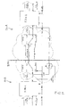
- a data transfer system 1 ( Figure 1) is provided for transferring data signals SGNL between a system input 31 and a system output 32. It comprises a first data consuming set 10 and a second data consuming set 20, as well as data transfer paths 30 between both sets 10 and 20.
- the first set 10 is designed to successively receive the data signals SGNL in an input form SGNL1 from the input 31, keep them inside after their writing therein, and provide them in a transfer form SGNL0 to the transfer paths 30 after their reading, for transmission to the second set 20.
- the second set 20 is designed to successively receive the data signals SGNL0 from the first set 10, keep them inside after their writing therein, and provide them in an output form SGNL2 to the output 32 after their reading.
- first set 10 and second set 20 comprise respective delaying units 15 and 25, able to delay in a desired way the time period between the reading of the data signals SGNL0 from the first set 10 and their writing to the second set 20 (which may include the reading in the first set 10, the transfer itself and/or the writing in the second set 20). They offer flexible tool for synchronization purpose.
- a specific feature of the data transfer system 1 is that read requests rd_req1, used internally in the first set 10 for triggering the reading of the data signals SGNL0 to be transferred, are transmitted to the second set 20 with the data signals SGNL0.
- the first set 10 and the transfer paths 30 are adapted for such an additional transmission, while the second set 20 is able to exploit the received read requests rd_req1 for synchronization between both sets 10 and 20.
- those received read requests rd_req1 can be used as write requests wr_req2 in the second set 20.
- This synchronization relies on a control unit CTRL belonging to the data transfer system 1, which is here represented ( Figure 1) in none of the sets 10 or 20.
- This control unit CTRL is in charge of exploiting control signals from the first and second sets 10 and 20, to appropriately control the execution of the read requests rd_req1 in the first set 10.
- the exploited control signals include the emptying state in the first set 10 ("empty”, “almost empty”) and the filling state in the second set 20 ('full", “almost full”). A very precise timing for writing the data signals SGNL0 in the second set 20 can thus be executed.
- control unit CTRL can be shared into two control sub-units respectively present in both sets 10 and 20. However, in preferred embodiments, it consists in a unique unit incorporated in only one of the sets 10 and 20. This leads to more simplicity and increased efficiency thanks to centralized control.
- the data transfer system 1 of Figure 1 will now be illustrated in two particular embodiments, in which the unique control unit CTRL is implemented respectively in the first set 10 and in the second set 20, as a hardware block forming a control logic unit.
- the first data consuming set 10, noted 10A consists in a first FPGA comprising a first FIFO noted FIFO1 and a first LVDS cell noted LVDS1 downstream the first FIFO.
- the second data consuming set 20, noted 20A consists in a second FPGA comprising a second FIFO noted FIF02 and a second LVDS cell noted LVDS2 upstream the second FIFO.
- the control unit CTRL, noted CTRL1 is implemented in the first set 10.
- the transfer paths 30 are represented as reduced to an FPGA interface noted IFA.
- Each of the FIFO components FIFO1 and FIF02 has a read port side and a write port side, able to be used with respective independent clocks. Thus, they are able to change a clock domain inside the data consuming set 10 or 20. Each of those ports is able to generate on its clock domain the following status signals:
- the parameter "word_number" can be generated twice, one for each clock domain.
- the status signal has a latency of 3 periods. It means for example, when the last word of the FIFO is read, that the control unit CTRL1 is informed that the FIFO is empty only 3 periods after the read request rd_req asserted to "1", namely with a signal active to high.
- the component FIFO1 of set 10 is exploited with one and same clock domain, which corresponds to a same first clock noted clk1 and used for writing (wr_clk1) as well as for reading (rd_clk1 that is the same as wr_clk1, the write and read ports being synchronous).
- the component FIF02 of set 20 is implemented with two clock domains, which correspond respectively to a second writing clock wr_clk2 and a second reading clock rd_clk2.
- the first FPGA transmitting
- a MAC layer which has its own clock clk1 provided by a local CPU (for "Central Processing Unit")
- the second FPGA transmits to a PHY layer, which must use another clock rd_clk2 for RF transmission.
- a proprietary hardware stores its data in the FIFO1 component using its write port, and on the receiving side, the proprietary hardware receives its data from the FIF02 component using its read port.
- the concerned input data signals SGNL1 (arriving as wr_data) and output data signals SGNL2 (leaving as rd_data) include in the illustration example, 199 signals (each signal can be a bit).
- the read request rd_req1 of the transmitting FIFO1 component is inserted with the data to transport, and is used as write request wr_req2 on the receiving FIF02 component, after transport through the LVDS cells LVDS1 and LVDS2.
- the data signals SGNL0 transferred between those two cells are made of 20x2 LVDS signals, including an additional couple of signals for the read request rd_req1 (couples of differential signals are used for high frequency transport of LVDS signals, like for example with RS-232 standard data interface; further, a factor 10 is applied to the data for LVDS processing).
- LVDS signals are also transmitted for clock data, consisting in the example illustration in 2 LVDS signals providing a frequency given by: Frd_clock 1 ⁇ 10 / a , where Frd_clock1 is the clock frequency for reading from the component FIFO1, and a is a predefined integer coefficient (introduced by the user, making transmission easier).
- the clock clk1 is regenerated at reception from those signals.
- the "almost full" signal of the component FIF02, noted wr_almost_full2 is set as described below. This enables to have an efficient control logic code while keeping the full bandwidth.
- the setup time consists in the minimum delay before the next clock count, while the hold time is the duration during which a signal has to be maintained at a same level after the clock count. Both setup and hold times have to be respected.
- the propagation time is not a multiple of the clock period (the setup and hold time would then not be respected), it is required to perform a change of clock domain of the signals.
- the times of setup and hold are respected, and it can be considered that the writing clock wr_clk2 for the FIF02 component is identical to the reading clock (which is also the writing clock) clk1 for the FIFO1 component. - namely, resync_latency is worth 0.
- the "almost full" signal of the receiving FIF02 component almost_full2 can be directly used for driving the read request signal rd_req1 of the transmitting FIFO1 component.
- the control unit CTRL1 During the process, if at one particular moment the number of words contained in the receiving FIF02 component is equal to: ( word_depth 2 - fifo_latency 2 - propagation_delay - resync_latency ) and if there is always a word ready to be transmitted from the transmitting FIFO1 component, then the control unit CTRL1 generates a number of consecutive read requests rd_req1 at the transmitting FIFO1 component which is equal to: ( fifo_latency 2 + propagation_delay + resync_latency ) because it is the time required for having an almost full signal wr_almost_full2 set to "1" at the receiving FIF02 component.
- the control unit CTRL1 When the wr_almost_full2 signal is set to "1", the control unit CTRL1 has to wait during a number of periods given by: ( fifo_latency 2 + propagation_delay + resync_latency ) between the previous asserted read request rd_req1 at the transmitting FIFO1 component and the check of the "full" signal at the receiving FIF02 component. After this number of periods, and if the "full” signal remains set to "0", then the control unit CTRL1 can set the read request signal rd_req1 to "1" for one period.
- the LVDS latency if 2 periods, the FIF02 latency fifo_latency2 is 3 periods, the FIFO1 latency fifo_latency1 is 1 period, the re-synchronization latency resync_latency is null (because the FPGAs are close) and the FIFO word depth word_depth1 or word_depth2 is 20 words for the FIFO1 or FIFO2 components, respectively.
- the first and second FPGAs are similar to the ones for the previous first embodiment. Thus, they comprise respectively the first and second data consuming sets 10 and 20, noted 10B and 20B, which include similar first and second FIFO, respectively FIFO1 and FIF02, and first and second LVDS cells, respectively LVDS1 and LVDS2, and are interconnected through an interface IFB.
- the control unit CTRL noted CTRL2 is here implemented in the second set 20.
- Table 1 Global latency for the whole data transfer system 1 From To Maximum latency Typical value wr_req2 full2, almost_full2 fifo_latency1 1 rd_req1 empty1, almost_empty1 fifo_latency2 3 wr_req2 empty1, almost_empty1 fifo_latency1 + propagation_delay + fifo_latency2 1 + 2 + 3 rd_req1 full2, almost_full2 fifo_latency1 + resync_latency + fifo_latency2 3 + 0 + 1
- the process takes into account the total propagation delay between the request to read a data from the transmitting FIFO1 component, and the update of status signals of the receiving FIF02 component.
- the programmer can take advantage of the timing of each status signal for optimising the hardware control logic.
Landscapes
- Engineering & Computer Science (AREA)
- Theoretical Computer Science (AREA)
- Computer Networks & Wireless Communication (AREA)
- Signal Processing (AREA)
- Physics & Mathematics (AREA)
- General Engineering & Computer Science (AREA)
- General Physics & Mathematics (AREA)
- Communication Control (AREA)
- Synchronisation In Digital Transmission Systems (AREA)
Priority Applications (4)
| Application Number | Priority Date | Filing Date | Title |
|---|---|---|---|
| EP05300031A EP1684164A1 (de) | 2005-01-13 | 2005-01-13 | Datenübertragungssystem |
| CNA200510137598XA CN1805330A (zh) | 2005-01-13 | 2005-12-30 | 数据传送系统及相关产品 |
| EP06100110A EP1684165A3 (de) | 2005-01-13 | 2006-01-05 | Datenübertragungssystem |
| US11/327,698 US8477768B2 (en) | 2005-01-13 | 2006-01-06 | Data transfer system and associated products |
Applications Claiming Priority (1)
| Application Number | Priority Date | Filing Date | Title |
|---|---|---|---|
| EP05300031A EP1684164A1 (de) | 2005-01-13 | 2005-01-13 | Datenübertragungssystem |
Publications (1)
| Publication Number | Publication Date |
|---|---|
| EP1684164A1 true EP1684164A1 (de) | 2006-07-26 |
Family
ID=34942491
Family Applications (1)
| Application Number | Title | Priority Date | Filing Date |
|---|---|---|---|
| EP05300031A Withdrawn EP1684164A1 (de) | 2005-01-13 | 2005-01-13 | Datenübertragungssystem |
Country Status (3)
| Country | Link |
|---|---|
| US (1) | US8477768B2 (de) |
| EP (1) | EP1684164A1 (de) |
| CN (1) | CN1805330A (de) |
Families Citing this family (2)
| Publication number | Priority date | Publication date | Assignee | Title |
|---|---|---|---|---|
| US7983373B2 (en) * | 2007-02-07 | 2011-07-19 | Vintomie Networks B.V., Llc | Clock distribution for 10GBase-T analog front end |
| US8904511B1 (en) * | 2010-08-23 | 2014-12-02 | Amazon Technologies, Inc. | Virtual firewalls for multi-tenant distributed services |
Family Cites Families (27)
| Publication number | Priority date | Publication date | Assignee | Title |
|---|---|---|---|---|
| JP3247377B2 (ja) * | 1992-04-13 | 2002-01-15 | セイコーエプソン株式会社 | 高密度バッファメモリアーキテクチャ及び方法 |
| US5884099A (en) * | 1996-05-31 | 1999-03-16 | Sun Microsystems, Inc. | Control circuit for a buffer memory to transfer data between systems operating at different speeds |
| US6249524B1 (en) * | 1997-03-19 | 2001-06-19 | Hitachi, Ltd. | Cell buffer memory for a large capacity and high throughput ATM switch |
| US5987543A (en) * | 1997-08-29 | 1999-11-16 | Texas Instruments Incorporated | Method for communicating digital information using LVDS and synchronous clock signals |
| US6611538B1 (en) * | 1999-05-27 | 2003-08-26 | 3Com Corporation | Data transmission synchronization system |
| US7301954B1 (en) * | 1999-09-24 | 2007-11-27 | United States Of America As Represented By The Secretary Of The Navy | Multiple-buffer queueing of data packets with high throughput rate |
| JP2001142845A (ja) * | 1999-11-17 | 2001-05-25 | Toshiba Corp | コンピュータシステムおよびデータ転送制御方法 |
| US7227918B2 (en) * | 2000-03-14 | 2007-06-05 | Altera Corporation | Clock data recovery circuitry associated with programmable logic device circuitry |
| JP3730846B2 (ja) * | 2000-08-10 | 2006-01-05 | 株式会社日立コミュニケーションテクノロジー | Atm通信装置およびatmセル転送制御方法 |
| US6977941B2 (en) * | 2000-11-08 | 2005-12-20 | Hitachi, Ltd. | Shared buffer type variable length packet switch |
| US7463626B2 (en) * | 2000-11-21 | 2008-12-09 | Roy Subhash C | Phase and frequency drift and jitter compensation in a distributed telecommunications switch |
| US6622222B2 (en) * | 2001-04-26 | 2003-09-16 | International Business Machines Corporation | Sequencing data on a shared data bus via a memory buffer to prevent data overlap during multiple memory read operations |
| US7123673B2 (en) * | 2001-07-19 | 2006-10-17 | Visteon Global Technologies, Inc. | System and method for transmission of digital information of varying sample rates over a synchronous network |
| US7646782B1 (en) * | 2001-07-30 | 2010-01-12 | Primrose Donald R | Data link/physical layer packet buffering and flushing |
| US6966009B1 (en) * | 2001-08-28 | 2005-11-15 | Tellabs Operations, Inc. | System and method for aligning data in a network environment |
| US6910092B2 (en) * | 2001-12-10 | 2005-06-21 | International Business Machines Corporation | Chip to chip interface for interconnecting chips |
| JP4082913B2 (ja) * | 2002-02-07 | 2008-04-30 | 株式会社ルネサステクノロジ | メモリシステム |
| US7073001B1 (en) * | 2002-04-03 | 2006-07-04 | Applied Micro Circuits Corporation | Fault-tolerant digital communications channel having synchronized unidirectional links |
| US6892287B1 (en) * | 2002-05-24 | 2005-05-10 | Xyratex Technology Limited | Frame reassembly in an ATM network analyzer |
| US7362771B1 (en) * | 2002-05-30 | 2008-04-22 | Marvell International Ltd. | Reduced latency FIFO |
| US7831653B2 (en) * | 2002-12-13 | 2010-11-09 | Lsi Corporation | Flexible template having embedded gate array and composable memory for integrated circuits |
| US7656905B2 (en) * | 2002-12-24 | 2010-02-02 | Samir Sheth | Apparatus and method for aggregation and transportation of gigabit ethernet and other packet based data formats |
| US7408878B2 (en) * | 2003-06-10 | 2008-08-05 | Cisco Technology, Inc. | System packet interface |
| JP2005004118A (ja) * | 2003-06-16 | 2005-01-06 | Hitachi Ltd | 表示装置 |
| US7937495B2 (en) * | 2003-06-25 | 2011-05-03 | Cisco Technology, Inc. | System and method for modifying data transferred from a source to a destination |
| US7606933B2 (en) * | 2004-02-11 | 2009-10-20 | Cray Canada Corporation | Shared memory and high performance communication using interconnect tunneling |
| US7254677B1 (en) * | 2004-05-04 | 2007-08-07 | Xilinx, Inc. | First-in, first-out memory system with reduced cycle latency |
-
2005
- 2005-01-13 EP EP05300031A patent/EP1684164A1/de not_active Withdrawn
- 2005-12-30 CN CNA200510137598XA patent/CN1805330A/zh active Pending
-
2006
- 2006-01-06 US US11/327,698 patent/US8477768B2/en not_active Expired - Fee Related
Non-Patent Citations (1)
| Title |
|---|
| LEVISON J ET AL: "An asynchronous communication protocol for internode connections in a scalable processor array", VLSI SIGNAL PROCESSING, VI, 1993., YWORKSHOP ON VELDHOVEN, NETHERLANDS 20-22 OCT. 1993, NEW YORK, NY, USA,IEEE, 20 October 1993 (1993-10-20), pages 489 - 497, XP010140377, ISBN: 0-7803-0996-0 * |
Also Published As
| Publication number | Publication date |
|---|---|
| CN1805330A (zh) | 2006-07-19 |
| US20070230503A1 (en) | 2007-10-04 |
| US8477768B2 (en) | 2013-07-02 |
Similar Documents
| Publication | Publication Date | Title |
|---|---|---|
| US10027433B2 (en) | Multiple clock domains in NoC | |
| US20180276159A1 (en) | System-on-chip and driving method thereof | |
| US7725625B2 (en) | Latency insensitive FIFO signaling protocol | |
| JPH03175848A (ja) | 2経路データ転送装置 | |
| KR20030045023A (ko) | Fifo 버퍼 및 이를 포함하는 통신 링크 및 데이터통신 방법 | |
| JPH06259225A (ja) | データ転送同期装置 | |
| US20150012718A1 (en) | System for compensating for dynamic skew in memory devices | |
| US20190197006A1 (en) | Scaling interface architecture between memory and programmable logic | |
| US8842492B2 (en) | Memory components and controllers that utilize multiphase synchronous timing references | |
| CN107145465A (zh) | 串行外设接口spi的传输控制方法、装置及系统 | |
| CN100426275C (zh) | 一种总线接口装置和方法 | |
| US6894531B1 (en) | Interface for a programmable logic device | |
| US6363076B1 (en) | Phantom buffer for interfacing between buses of differing speeds | |
| US20180013689A1 (en) | Circuit and method for credit-based flow control | |
| US8477768B2 (en) | Data transfer system and associated products | |
| EP1684165A2 (de) | Datenübertragungssystem | |
| US6839859B2 (en) | Semiconductor integrated circuit having clock synchronous type circuit and clock non-synchronous type circuit | |
| US6282149B1 (en) | Circuit and method for synchronized data banking | |
| JPWO2016158063A1 (ja) | 非同期インタフェース | |
| US20170126427A1 (en) | Motor controller attaining both low latency and high throughput data communications | |
| US7899955B2 (en) | Asynchronous data buffer | |
| US20250036159A1 (en) | Clock domain crossing synchronization circuits and methods to guarantee proper data signal order | |
| US20140143462A1 (en) | Register slicing circuit and system on chip including the same | |
| US20170078080A1 (en) | Dual Path Source Synchronous Interface | |
| KR101999125B1 (ko) | Rs-422와 rs-485 시리얼 통신을 위한 출력신호 자동 제어기 |
Legal Events
| Date | Code | Title | Description |
|---|---|---|---|
| PUAI | Public reference made under article 153(3) epc to a published international application that has entered the european phase |
Free format text: ORIGINAL CODE: 0009012 |
|
| AK | Designated contracting states |
Kind code of ref document: A1 Designated state(s): AT BE BG CH CY CZ DE DK EE ES FI FR GB GR HU IE IS IT LI LT LU MC NL PL PT RO SE SI SK TR |
|
| AX | Request for extension of the european patent |
Extension state: AL BA HR LV MK YU |
|
| AKX | Designation fees paid | ||
| REG | Reference to a national code |
Ref country code: DE Ref legal event code: 8566 |
|
| STAA | Information on the status of an ep patent application or granted ep patent |
Free format text: STATUS: THE APPLICATION IS DEEMED TO BE WITHDRAWN |
|
| 18D | Application deemed to be withdrawn |
Effective date: 20070127 |