EP1686366A2 - Dispositif de résonance plasmonique de surface longue portée en utilisant un matériau diélectrique poreux en échelle nanométrique et méthode pour le fabriquer - Google Patents
Dispositif de résonance plasmonique de surface longue portée en utilisant un matériau diélectrique poreux en échelle nanométrique et méthode pour le fabriquer Download PDFInfo
- Publication number
- EP1686366A2 EP1686366A2 EP05017910A EP05017910A EP1686366A2 EP 1686366 A2 EP1686366 A2 EP 1686366A2 EP 05017910 A EP05017910 A EP 05017910A EP 05017910 A EP05017910 A EP 05017910A EP 1686366 A2 EP1686366 A2 EP 1686366A2
- Authority
- EP
- European Patent Office
- Prior art keywords
- plasmon resonance
- surface plasmon
- dielectric layer
- porous dielectric
- resonance device
- Prior art date
- Legal status (The legal status is an assumption and is not a legal conclusion. Google has not performed a legal analysis and makes no representation as to the accuracy of the status listed.)
- Withdrawn
Links
Images


Classifications
-
- G—PHYSICS
- G01—MEASURING; TESTING
- G01N—INVESTIGATING OR ANALYSING MATERIALS BY DETERMINING THEIR CHEMICAL OR PHYSICAL PROPERTIES
- G01N21/00—Investigating or analysing materials by the use of optical means, i.e. using sub-millimetre waves, infrared, visible or ultraviolet light
- G01N21/17—Systems in which incident light is modified in accordance with the properties of the material investigated
- G01N21/55—Specular reflectivity
- G01N21/552—Attenuated total reflection
- G01N21/553—Attenuated total reflection and using surface plasmons
Definitions
- the present invention relates to a long-range surface plasmon resonance device utilizing a nano-scale porous dielectric and a method of fabricating the same, and more particularly, to a long-range surface plasmon resonance device having high resolution and high sensitivity by properly adjusting a refractive index of a porous dielectric and a size and density of porosities formed in a porous dielectric layer and to a method of fabricating such a long-range surface plasmon resonance device.
- Fluorescence analysis has been widely used as a biosample analysis method.
- each of the biomolecules is first colored by a fluorescent dye having a typical reaction wavelength and information such as an ingredient of the biosample is then analyzed from a spectrum of light emitted from the sample by irradiating light to the biosample mixed with a variety of biomolecules.
- the fluorescence analysis has problems in that the coloring process for the biosample is complicated and the fluorescent dye is very expensive.
- a variety of methods for analyzing the biomolecules without using the fluorescent dye have been developed.
- One of them is a method using surface plasmon resonance.
- the plasmon is a kind of surface electromagnetic waves traveling along interface surfaces between a thin metal layer and a dielectric and a surface plasmon resonance phenomenon is produced by a charge density oscillation generated on a surface of the thin metal layer.
- FIG. 1 shows a conventional structure incurring such surface plasmon resonance.
- a prism 10 and a thin metal layer 12 are respectively attached on bottom and top surfaces of a transparent substrate 11 and a fluid sample 13 to be measured is disposed on the thin metal layer 12.
- the transparent substrate 11 and the prism 10 are formed of materials having the same refractive index.
- a total reflection is generated when light is directed to the boundary surface between the thin metal layer 12 and the transparent substrate 11 at an angle greater than a total reflection angle.
- an evanescent wave having a very short effective length is generated and advances from the reflective surface to the thin metal layer 12. Since a thickness of the thin metal layer 12 is less than the effective length of the evanescent wave, the evanescent wave can reach the liquid sample disposed on the thin metal layer 12.
- the wavelength of the incident light is continuously varied, the light is absorbed at a specific wavelength and a charge density oscillation appears on the surface of the thin metal layer 12. This is called an excitation of the surface plasmon.
- This phenomenon may be generated at a specific incident angle when the light incident angle is continuously varied instead of varying the wavelength.
- the wavelength or incident angle when the surface plasmon is excited is determined by the refraction index of the liquid sample 13.
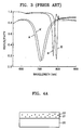
- FIG. 3 shows a graph illustrating variation of the reflectivity according to the variation of the wavelength.
- a reflectivity curve indicated by the reference character A is a case where the liquid sample 13 is water. This shows that the surface plasmon resonance is generated at a wavelength of about 700nm and the reflectivity is steeply reduced.
- the refractive index varies by dissolving a biomaterial in the water
- the resonance wavelength varies as indicated by a reflectivity A'.
- FIG. 2 shows a structure for solving the above-described problem.
- a buffer layer 14 formed of dielectric is disposed between a transparent substrate 11 and a thin metal layer 12.
- the effective length of the evanescent wave is increased, it becomes possible to measure a relative large sample. This is called a long-range surface plasmon resonance.
- reflective curves B and B' of FIG. 3 since a very sharp reflective curve is formed, higher resolution and sensitivity can be obtained.
- the reflectivity curve B is for a case where the liquid sample 13 is pure water and the reflectivity curve B' is for a case where there is refractive index is varied by adding other material to the water.
- the curves B and B' are very sharp.
- the buffer layer 14 should be made of a transparent material that can be coated on the transparent substrate 11 while having a refractive index similar to that of the liquid sample so that the surface plasmon resonance can be generated.
- Teflon and MgF 2 that can satisfy the above conditions.
- Teflon and MgF 2 that can satisfy the above conditions.
- an optimal reflectivity curve cannot be provided according to the liquid sample. That is, even when the reflective curve becomes sharp, noise increases by outer conditions, thereby making it difficult to actually improve the resolution.
- the present invention provides a surface plasmon resonance device including a buffer layer having a properly adjusted refractive index. That is, the present invention provides a long-range surface plasmon resonance device that can provide optimum detection conditions by properly adjusting a refractive index of the buffer layer using a nano-scale porous dielectric and a method of fabricating such a long-range surface plasmon resonance device.
- a surface plasmon resonance device comprising: a transparent substrate; a porous dielectric layer formed on a top surface of the transparent substrate; a thin metal layer formed on the porous dielectric layer; and a prism attached on a bottom surface of the transparent layer.
- the porous dielectric layer may have an adjusted refractive index obtained by adjusting a density of porosities formed in the porous dielectric layer.
- the porous dielectric layer may be formed by vaporizing porogen through a heat treatment after the porogen is dispersed in a dielectric material.
- the dielectric material may contain at least one of silane and siloxane polymer and the porogen may contain cyclodextrin.
- a size of each porosity formed in the porous dielectric layer may be less than 10nm.
- the thin metal layer may contain Au and a thickness of the thin metal layer may be less than 20nm.
- the prism may have a refractive index identical to that of the transparent substrate.
- a method for fabricating a surface plasmon resonance device including: mixing and dispersing porogen with and in a dielectric material; depositing the dielectric material mixed with the porogen on a transparent substrate to a predetermined thickness; performing a heat treatment to form a porous dielectric layer by crystallizing the dielectric material and vaporizing the porogen dispersed in the dielectric material; depositing a thin metal layer on the porous dielectric layer; and attaching a prism on a bottom surface of the transparent substrate.
- a mixture ratio of the dielectric material and the porogen may be determined according to parameters of the surface plasmon resonance device that is optimized according to a sample that is to be measured.
- the parameters may include a refractive index of the porous dielectric layer, a thickness of the porous dielectric layer, a refractive index of the transparent substrate, a thickness of the thin metal layer, and a wavelength of a light source.
- a mixture ratio of the dielectric material and the porogen may be determined according to a refractive index of the porous dielectric layer.
- the heat treatment may be performed at 450 °C.
- Porous dielectric is well known as a material that can realize the need.
- the porogen is vaporized through a heat treatment. As the porogen is vaporized, spaces where the porogen exists are hollowed so that a plurality of micro-porosities are formed in the dielectric. At this point, according to the ratio of the porogen to the dielectric, a refractive index of the resultant porous dielectric is varied.
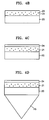
- FIGS. 4A through 4D show a method of fabricating a long-range surface plasmon resonance device using the above-described principle.
- a dielectric layer 21 in which porogen 22 is dispersed is formed on a transparent substrate 20 such as glass.
- a transparent substrate 20 such as glass.
- dielectric have a dielectric constant less than 3.
- silane or siloxane polymer may be used. That is, silane-gel or siloxane polymer in which the porogen 22 is dispersed is deposited on the transparent substrate 20, thereby obtaining a structure as shown in FIG. 4A.
- the dielectric layer 21 formed of the silan-gel or siloxane polymer When the dielectric layer 21 formed of the silan-gel or siloxane polymer is heat-processed at a temperature of 450°C , the dielectric layer 21 starts crystallizing. In this process, the porogen 22 dispersed in the dielectric layer 21 is vaporized to evacuate the dielectric layer 21, thereby forming a plurality of porosities 23 in the dielectric layer 21 as depicted in FIG. 4B.
- the porous dielectric layer 21 functions as a buffer layer generating a long-range surface plasmon resonance.
- a thin metal layer 24 is deposited on the porous dielectric layer 21 and a prism 25 is attached on a bottom of the transparent substrate 20.
- the thin metal layer 24 may be formed of Au.
- a thickness of the thin metal layer 24 should be less than an effective distance of the evanescent wave generated on a boundary surface between the substrate 20 and the porous dielectric layer 21.
- a preferable thickness of the thin metal layer 24 is less than 20nm.
- the prism 25 may be formed of a material identical to that of the transparent substrate 20.
- a binder such as index matching fluid and transparent elastomer attaching the prism 25 to the transparent substrate 20 is formed of a material having a refractive index identical to those of the prism 25 and the transparent substrate 20.
- the porous dielectric layer 21 on which the metal layer 24 will be deposited should have a very even surface.
- the metal layer 24 may not be effectively deposited on the porous dielectric layer 21.
- a size of each groove formed on the surface of the porous dielectric layer 21 is too large, it is difficult to uniformly apply the thin metal layer 24 on the porous dielectric layer 21. In this case, a surface plasmon resonance condition may vary and the surface plasmon resonance may not appear according to a light incident location.
- a diameter of each porosity formed in and on the dielectric layer 21 should be greatly less than a thickness of the thin metal layer 24. That is, the porous dielectric layer 21 should be designed to have porosities of a nano-scale diameter. Therefore, the porogen should be formed of an organic material having particles having a very small diameter and capable of being uniformly dispersed in the dielectric. As the porogen satisfying such conditions, cyclodextrin (CD) may be used. In this case, a diameter of each porosity formed in the dielectric layer may be less than 2nm.
- the refractive index of the porous dielectric layer 21 may be varied according to a proportion of the porogen. That is, the refractive index of the porous dielectric layer 21 is varied according to a density of the porosities formed in the porous dielectric layer 21. Therefore, after determining in advance an optimum refractive index of the porous dielectric layer, which is proper to the liquid sample that is to be detected, the proportion of the porogen is adjusted such that the porous dielectric layer 21 can have the optimum refractive index.
- Table 1 shows a variation of the refractive index according to a ratio of the dielectric material to the porogen in the case where cyclic silsesquioxane (CSSQ) is used as the dielectric material and the CD is used as the porogen.
- the proportion of the porogen is increased (a density of the porosities formed in the dielectric layer is increased), and the refractive index is reduced.
- a refractive index of pure CSSQ is 1.433.
- a refractive index of porous CSSQ formed using 50wt% CD is reduced to 1.315.
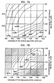
- FIG. 5 shows a simulation graph illustrating a reflectivity-sensitivity when thicknesses of the porous dielectric layer 21 and the thin metal layer 24 are varied in a state where a refractive index of the porous dielectric layer 21 is fixed
- the reflectivity-sensitivity represents a variation of an intensity of light at half-width when the reflectivity curve is shifted due to the refractive index variation of the liquid sample.
- FIG. 6 when the light incident angle at the boundary surface between the transparent substrate 20 and the porous dielectric layer through the prism 25 is varied from 63° to 65° , an initial reflectivity of the liquid sample is exampled in a left side of the curve.
- the refractive index of the sample is varied to move the reflectivity curve rightward. Accordingly, the intensity of the reflected light at an incident angle corresponding to the half-width of the initial reflectivity curve is increased by C.
- the reflectivity-sensitivity can be defined as a variation amount of the reflectivity at the half-width per a variation amount of the refractive index.
- "/RIU(refractive index unit)" is used as a unit of the reflectivity-sensitivity.
- FIG. 5 shows a simulation result when water (having a reflective index n of 1.333) is used as the liquid test solution, Au is used as a thin metal layer 24, a refractive index n of the porous dielectric layer 21 is 1.333, an inner angle of the prism is 60° , and a refractive index n of the prism at a 632.8nm wavelength is 1.51509.
- FIGS. 7A and 7B show a simulation result of the variation of the reflectivity-sensitivity according to the variations of a thickness and refractive index of the porous dielectric layer 21 in a state where a thickness of the metal layer 24 is fixed at 20nm.
- the reflectivity-sensitivity is increased as it goes toward the center of the graph. That is, while a thickness of the porous dielectric layer 21 is varied from 800nm to 1400nm, the reflectivity-sensitivity is gradually increased and then gradually decreased.
- a refractive index is varied from 1.31 to 1.36, the reflectivity-sensitivity is gradually increased and then gradually decreased.
- FIG. 7B shows an enlarge graph of a thickness section from 1050nm to 1350nm of the porous dielectric layer 21 and a refractive index section from 1.333 to 1.355 of the porous dielectric layer 21.
- a thickness and refractive index of the porous dielectric layer 21 are respectively 1300nm and 1.35, the reflectivity-sensitivity becomes maximized.
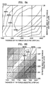
- FIGS. 8A and 8B show a simulation result of the variation of the reflectivity-sensitivity according to the variations of a thickness and refractive index of the porous dielectric layer 21 in a state where a thickness of the metal layer 24 is fixed at 12nm.
- FIG. 8A it can be noted that the reflectivity-sensitivity is increased as it goes toward the center of the graph.
- FIG. 8B shows an enlarge graph of a thickness section from 1500nm to 2000nm of the porous dielectric layer 21 and a refractive index section from 1.329 to 1.339 of the porous dielectric layer 21. As shown in FIG.
- the reflectivity-sensitivity becomes maximized.
- the maximum value of the reflectivity-sensitivity is about 600/RIU greater than 178/RIU that is a maximum value obtained when the thickness of the thin metal layer 24 is 20nm.
- the long-range surface plasmon resonance device can be fabricated according to the optimized refractive index and thickness.
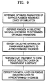
- FIG. 9 shows a flowchart illustrating a method of fabricating a long-range surface plasmon resonance device.
- a variety of optimized parameters of the long-range surface plasmon resonance are first determined according to the samples through by a simulation. For example, a variety of optimized parameters such as a thickness of the thin metal layer 24, a thickness of the porous dielectric layer 21, a refractive index of the porous dielectric layer 21, a material of the thin metal layer 24, materials of the transparent substrate 20 and the prism 25, a wavelength of the light source, and the like are determined. Then, as illustrated with reference to FIGS.
- the porogen 22 is mixed with and dispersed in the dielectric material at a predetermined ratio and deposited on the transparent substrate 20 to provide a desired refractive index. Then, a heat treatment is performed to crystallize the dielectric material and remove the porogen 22 from the dielectric material, thereby forming the porous dielectric layer 21.
- the thin metal layer 24 having a predetermined thickness calculated in advance is deposited on the porous dielectric layer 21 and the prism is attached on the transparent substrate 20, thereby providing an optimized long-range surface plasmon resonance device.
- the present invention it is possible to properly adjust the refractive index of the buffer layer. Therefore, an optimized long-range surface plasmon resonance device can be fabricated. As a result, it is possible to obtain high resolution as well as high sensitivity. Furthermore, it is possible to detect even a micro-variation of the refractive index of the liquid sample. Therefore, it is possible to detect even a very small amount of material contained in the liquid sample.
- the solvent of the samples is not limited to the water. That is, it becomes possible to fabricate a surface plasmon resonance device that is capable of detecting samples using other types of solvents in addition to water.
Landscapes
- Physics & Mathematics (AREA)
- Health & Medical Sciences (AREA)
- Life Sciences & Earth Sciences (AREA)
- Chemical & Material Sciences (AREA)
- Analytical Chemistry (AREA)
- Biochemistry (AREA)
- General Health & Medical Sciences (AREA)
- General Physics & Mathematics (AREA)
- Immunology (AREA)
- Pathology (AREA)
- Investigating Or Analysing Materials By Optical Means (AREA)
- Optical Modulation, Optical Deflection, Nonlinear Optics, Optical Demodulation, Optical Logic Elements (AREA)
Applications Claiming Priority (1)
| Application Number | Priority Date | Filing Date | Title |
|---|---|---|---|
| KR20050008345A KR100723401B1 (ko) | 2005-01-29 | 2005-01-29 | 나노 크기의 다공성 재료를 이용한 표면 플라즈몬 공명소자 및 그 제조방법 |
Publications (2)
| Publication Number | Publication Date |
|---|---|
| EP1686366A2 true EP1686366A2 (fr) | 2006-08-02 |
| EP1686366A3 EP1686366A3 (fr) | 2008-11-05 |
Family
ID=36204360
Family Applications (1)
| Application Number | Title | Priority Date | Filing Date |
|---|---|---|---|
| EP20050017910 Withdrawn EP1686366A3 (fr) | 2005-01-29 | 2005-08-17 | Dispositif de résonance plasmonique de surface longue portée en utilisant un matériau diélectrique poreux en échelle nanométrique et méthode pour le fabriquer |
Country Status (4)
| Country | Link |
|---|---|
| US (1) | US7286235B2 (fr) |
| EP (1) | EP1686366A3 (fr) |
| JP (1) | JP4045287B2 (fr) |
| KR (1) | KR100723401B1 (fr) |
Cited By (2)
| Publication number | Priority date | Publication date | Assignee | Title |
|---|---|---|---|---|
| CN101936899A (zh) * | 2010-07-29 | 2011-01-05 | 华东师范大学 | 一种长程表面等离子体共振传感器及制备方法 |
| CN101598665B (zh) * | 2009-06-03 | 2011-04-06 | 南京航空航天大学 | 基于内置调制层的棱镜spr传感器检测系统 |
Families Citing this family (11)
| Publication number | Priority date | Publication date | Assignee | Title |
|---|---|---|---|---|
| JP2007033342A (ja) * | 2005-07-28 | 2007-02-08 | Sumitomo Electric Ind Ltd | 分析デバイスおよび分析装置 |
| US7583882B2 (en) * | 2006-11-10 | 2009-09-01 | University Of Alabama In Huntsville | Waveguides for ultra-long range surface plasmon-polariton propagation |
| KR101000675B1 (ko) | 2008-08-07 | 2010-12-10 | 연세대학교 산학협력단 | 표면 플라즈몬 공명을 이용한 나노 스케일 간극 측정장치및 이를 이용한 나노 스케일 간극 측정방법 |
| KR101669219B1 (ko) | 2010-12-30 | 2016-10-26 | 삼성전자주식회사 | 광변조기 및 이를 채용한 광학장치 |
| CN103620387B (zh) * | 2011-06-16 | 2017-02-15 | 3M创新有限公司 | 表面等离子体共振传感器元件和包括其的传感器 |
| JP2013181753A (ja) * | 2012-02-29 | 2013-09-12 | Nitto Denko Corp | Sprセンサセルおよびsprセンサ |
| JP5949905B2 (ja) * | 2012-03-26 | 2016-07-13 | コニカミノルタ株式会社 | プリズム及びセンサーチップ |
| KR101939304B1 (ko) * | 2017-07-20 | 2019-01-16 | 한국식품연구원 | 테라헤르츠파 저역 통과 필터 및 테라헤르츠파 저역 통과 필터 제조 방법 |
| KR102143688B1 (ko) * | 2018-06-27 | 2020-08-11 | 한양대학교 에리카산학협력단 | 개질된 표면을 가지는 다공성 구조체, 경화 패턴을 가지는 다공성 구조체 및 그 제조 방법들 |
| KR102159437B1 (ko) * | 2018-11-09 | 2020-09-23 | 한양대학교 에리카산학협력단 | 다공성 탄성 구조체, 표면이 개질된 다공성 탄성 구조체, 및 그들의 제조 방법. |
| CN110987889A (zh) * | 2019-12-16 | 2020-04-10 | 长沙学院 | 一种表面等离子增强荧光成像传感器及其测量方法 |
Family Cites Families (12)
| Publication number | Priority date | Publication date | Assignee | Title |
|---|---|---|---|---|
| GB8813307D0 (en) * | 1988-06-06 | 1988-07-13 | Amersham Int Plc | Biological sensors |
| WO1992021976A1 (fr) * | 1991-06-04 | 1992-12-10 | Fisons Plc | Dispositif d'analyse |
| JPH05327225A (ja) * | 1992-05-26 | 1993-12-10 | Nec Corp | 多層印刷配線板 |
| US5327225A (en) * | 1993-01-28 | 1994-07-05 | The Center For Innovative Technology | Surface plasmon resonance sensor |
| FR2707007B1 (fr) * | 1993-06-24 | 1995-08-25 | France Etat Armement | |
| US5991488A (en) * | 1996-11-08 | 1999-11-23 | The Arizona Board Of Regents On Behalf Of The University Of Arizona | Coupled plasmon-waveguide resonance spectroscopic device and method for measuring film properties |
| JPH10267841A (ja) * | 1997-03-24 | 1998-10-09 | Kokuritsu Shintai Shogaisha Rehabilitation Center Souchiyou | 表面プラズモン共鳴センシングデバイス |
| US6787601B2 (en) * | 2001-03-26 | 2004-09-07 | Shipley Company, L.L.C. | Polymer synthesis |
| JP2004016609A (ja) * | 2002-06-19 | 2004-01-22 | Omron Healthcare Co Ltd | 体液成分濃度測定方法及び体液成分濃度測定装置 |
| KR100533538B1 (ko) * | 2002-12-03 | 2005-12-05 | 삼성전자주식회사 | 새로운 기공형성물질을 포함하는 다공성 층간 절연막을형성하기 위한 조성물 |
| KR100588987B1 (ko) * | 2003-05-29 | 2006-06-13 | 케이맥(주) | 표면 플라즈몬 공명현상을 이용한 광학적 분석장치 및 그 분석방법 |
| JP4465233B2 (ja) * | 2003-06-30 | 2010-05-19 | 三星電子株式会社 | 多官能性環状シロキサン化合物、この化合物から製造されたシロキサン系重合体及びこの重合体を用いた絶縁膜の製造方法 |
-
2005
- 2005-01-29 KR KR20050008345A patent/KR100723401B1/ko not_active Expired - Fee Related
- 2005-08-17 EP EP20050017910 patent/EP1686366A3/fr not_active Withdrawn
- 2005-08-17 US US11/205,995 patent/US7286235B2/en not_active Expired - Fee Related
-
2006
- 2006-01-10 JP JP2006002932A patent/JP4045287B2/ja not_active Expired - Fee Related
Cited By (2)
| Publication number | Priority date | Publication date | Assignee | Title |
|---|---|---|---|---|
| CN101598665B (zh) * | 2009-06-03 | 2011-04-06 | 南京航空航天大学 | 基于内置调制层的棱镜spr传感器检测系统 |
| CN101936899A (zh) * | 2010-07-29 | 2011-01-05 | 华东师范大学 | 一种长程表面等离子体共振传感器及制备方法 |
Also Published As
| Publication number | Publication date |
|---|---|
| KR20060087314A (ko) | 2006-08-02 |
| KR100723401B1 (ko) | 2007-05-30 |
| JP4045287B2 (ja) | 2008-02-13 |
| US20060170927A1 (en) | 2006-08-03 |
| US7286235B2 (en) | 2007-10-23 |
| EP1686366A3 (fr) | 2008-11-05 |
| JP2006208375A (ja) | 2006-08-10 |
Similar Documents
| Publication | Publication Date | Title |
|---|---|---|
| Seo et al. | Terahertz biochemical molecule‐specific sensors | |
| TWI468668B (zh) | 局部表面電漿共振感應器晶片及其使用與製造方法 | |
| EP1686366A2 (fr) | Dispositif de résonance plasmonique de surface longue portée en utilisant un matériau diélectrique poreux en échelle nanométrique et méthode pour le fabriquer | |
| GB2525854B (en) | Sensing methods and apparatus | |
| KR101279419B1 (ko) | 고민감도 국소 표면 플라즈몬 공진 센서 및 이를 이용한 센서 시스템 | |
| US20090213384A1 (en) | Sensor, multichannel sensor, sensing apparatus, and sensing method | |
| US20090046350A1 (en) | Photonic crystal mirrors for high-resolving-power fabry perots | |
| Ghasemi et al. | Biosensing applications of all-dielectric SiO2-PDMS meta-stadium grating nanocombs | |
| KR20050084016A (ko) | 전자기장 분포 발생 방법 | |
| CN113390819B (zh) | 一种太赫兹传感器 | |
| Anopchenko et al. | Effect of thickness disorder on the performance of photonic crystal surface wave sensors | |
| Kassa-Baghdouche | Optical properties of a point-defect nanocavity-based elliptical-hole photonic crystal for mid-infrared liquid sensing | |
| CN1611927A (zh) | 用于生物和化学试剂的超高灵敏度光学检测的方法和装置 | |
| US8649000B1 (en) | Whispering gallery optical resonator spectroscopic probe and method | |
| CN114325897B (zh) | 一种基于渐变周期增强太赫兹光谱吸收的介质超材料 | |
| CN103439308A (zh) | 一种表面增强拉曼基底及其制备方法 | |
| Wang et al. | Rapid analysis of a doxycycline hydrochloride solution by metallic mesh device-based reflection terahertz spectroscopy | |
| Jamil et al. | Graphene-MoS 2 SPR-based biosensor for urea detection | |
| Mahmud et al. | Dual-side polished SPR-PCF ultra-wide refractive index sensor with high amplitude sensitivity | |
| CN111337445B (zh) | 一种基于角度扫描增强红外光谱吸收的介质超表面 | |
| Oh et al. | High sensitive SERS film of Ag-coated aggregated nanowire structure and benzene gas detection | |
| Saad et al. | Theoretical evaluation of a fiber-optic SPR biosensor based on a gold layer treated with thiol acid | |
| Mizaikoff | Mid-infrared fiber optic sensors: Potential and perspectives | |
| CN109696419B (zh) | 一种检测深度可调的lrspr传感器折射率变化测量方法 | |
| Nguyen et al. | Cascaded nano-porous silicon for high sensitive biosensing and functional group distinguishing by Mid-IR spectra |
Legal Events
| Date | Code | Title | Description |
|---|---|---|---|
| PUAI | Public reference made under article 153(3) epc to a published international application that has entered the european phase |
Free format text: ORIGINAL CODE: 0009012 |
|
| 17P | Request for examination filed |
Effective date: 20050817 |
|
| AK | Designated contracting states |
Kind code of ref document: A2 Designated state(s): AT BE BG CH CY CZ DE DK EE ES FI FR GB GR HU IE IS IT LI LT LU LV MC NL PL PT RO SE SI SK TR |
|
| AX | Request for extension of the european patent |
Extension state: AL BA HR MK YU |
|
| PUAL | Search report despatched |
Free format text: ORIGINAL CODE: 0009013 |
|
| AK | Designated contracting states |
Kind code of ref document: A3 Designated state(s): AT BE BG CH CY CZ DE DK EE ES FI FR GB GR HU IE IS IT LI LT LU LV MC NL PL PT RO SE SI SK TR |
|
| AX | Request for extension of the european patent |
Extension state: AL BA HR MK YU |
|
| STAA | Information on the status of an ep patent application or granted ep patent |
Free format text: STATUS: THE APPLICATION HAS BEEN WITHDRAWN |
|
| AKX | Designation fees paid | ||
| 18W | Application withdrawn |
Effective date: 20090603 |
|
| REG | Reference to a national code |
Ref country code: DE Ref legal event code: 8566 |