EP1688824A1 - Leistungsregelungsschaltung zur Erkennung unterschiedlicher Arten von variablen Gleichstromsquellen - Google Patents
Leistungsregelungsschaltung zur Erkennung unterschiedlicher Arten von variablen Gleichstromsquellen Download PDFInfo
- Publication number
- EP1688824A1 EP1688824A1 EP05011428A EP05011428A EP1688824A1 EP 1688824 A1 EP1688824 A1 EP 1688824A1 EP 05011428 A EP05011428 A EP 05011428A EP 05011428 A EP05011428 A EP 05011428A EP 1688824 A1 EP1688824 A1 EP 1688824A1
- Authority
- EP
- European Patent Office
- Prior art keywords
- variable output
- power source
- power
- circuitry
- control circuitry
- Prior art date
- Legal status (The legal status is an assumption and is not a legal conclusion. Google has not performed a legal analysis and makes no representation as to the accuracy of the status listed.)
- Granted
Links
Images

Classifications
-
- G—PHYSICS
- G06—COMPUTING OR CALCULATING; COUNTING
- G06F—ELECTRIC DIGITAL DATA PROCESSING
- G06F1/00—Details not covered by groups G06F3/00 - G06F13/00 and G06F21/00
- G06F1/26—Power supply means, e.g. regulation thereof
- G06F1/263—Arrangements for using multiple switchable power supplies, e.g. battery and AC
Definitions
- This disclosure relates to variable output direct current (DC) power sources, and, in particular, to power control circuitry that can automatically detect a type of a variable output DC power source.
- DC direct current
- variable output DC power sources may accept an unregulated input voltage and provide a variable output DC voltage and output current to a load.
- the unregulated input voltage may be an alternating current (AC) or DC input voltage.
- variable output DC power sources There are many different classes of variable output DC power sources that may be defined by parameters including, but not limited to, input voltage range, maximum output voltage, and maximum output current. Within each class, there may be differing types of variable output DC power sources. Each type may be defined by additional parameters including, but not limited to, maximum output power rating, load regulation, line regulation, and over voltage/current protection features. In a conventional arrangement, each type of variable output DC power source may be designed to couple to particular power control circuitry to control operations thereof. This conventional arrangement decreases design flexibility and increases costs as each variable output DC power source requires particular power control circuitry.
- the method may include coupling a variable output DC power source to power control circuitry, and detecting a type of the variable output DC power source in response to the coupling operation.
- the system may include a variable output DC power source and power control circuitry.
- the power control circuitry may be configured to detect a type of the variable output DC power source in response to a coupling of the variable output DC power source to the power control circuitry.
- the power control circuitry may include source type recognition circuitry configured to detect a type of a variable output DC power source in response to a coupling of the variable output DC power source to the power control circuitry.
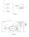
- FIG. 1 illustrates a system 100 including a plurality of variable output DC power sources 102-1, 102-2, and 102-3 and power control circuitry 104 consistent with embodiments herein.
- circuitry may comprise, for example, singly or in any combination, hardwired circuitry, programmable circuitry, state machine circuitry, and/or firmware that stores instructions executed by programmable circuitry.
- Each variable output DC power source (VOPS) 102-1, 102-2, and 102-3 may be in the same class of variable output DC power sources.
- a class may be defined by parameters including, but not limited to, input voltage range, maximum output voltage, and maximum output current.
- a class of variable output DC power sources may be physically capable of being coupled to the power control circuitry 104.
- Each type may be defined by additional parameters including, but not limited to, a maximum output power rating, load regulation, line regulation, and over voltage/current protection features.
- Each VOPS 102-1, 102-2, and 102-3 may be individually coupled to the power control circuitry 104.
- the power control circuitry may be configured to detect which type of VOPS has been coupled to it. For example, if the VOPS 102-1 is coupled to the power control circuitry 104, the power control circuitry 104 may detect that a "Type A" VOPS is coupled to it. The power control circuitry 104 may then be able to control the VOPS 102-1 with particulars associated with a "Type A" VOPS. Similarly, if the VOPS 102-2 is coupled to the power control circuitry 104, the power control circuitry may detect that a "Type B" VOPS is coupled to it.
- the power control circuitry 104 may then be able to control the VOPS 102-2 with particulars associated with a "Type B" VOPS. Only three types of variable output DC power sources are illustrated in FIG. 1 for clarity of illustration. However, the power control circuitry 104 may be configured to detect any plurality of differing types of variable output DC power sources in a variety of different classes of variable output DC power sources.
- the power control circuitry 104 may send an interrogation signal to the VOPS after the coupling of the VOPS to the power control circuitry 104.
- the power control circuitry 104 may then evaluate a response to the interrogation signal to determine the type of VOPS.
- the interrogation signal may be a current signal or a voltage signal as further detailed herein relative to different embodiments.
- FIG. 2 illustrates a system 200 having the VOPS 102-1 (Type A) and the power control circuitry 104 of FIG. 1 coupled together.
- the system 200 may include a power source 210, the VOPS 102-1, and an electronic device 203.
- the electronic device 203 may include a load 208 and the power control circuitry 104.
- the power control circuitry 104 may be stand alone circuitry or may be part of a more complex controller 218.
- the power source 210 may be capable of supplying an AC or DC input voltage to the VOPS 102-1.
- the VOPS 102-1 may accept input power from the power source 210 and provide power to the load 208.
- the electronic device 203 may include, but not be limited to, a server computer, a desk top computer, a laptop computer, a cell phone, a personal digital assistant, a digital camera, etc.
- the load 208 may represent the load of the entire electronic device 203 or a part of the electronic device 203.
- the load 208 may also represent a stand alone load which is not part of the electronic device 203.
- FIG. 2 illustrates only one of many possible topologies or systems since, for example, in other instances the VOPS 102-I may be part of the electronic device 203.
- the power source 210 may be a common 120 volt/60 Hertz AC power line
- the VOPS 102-1 may be a variable output ACDC adapter
- the electronic device 203 may be a laptop computer
- the load 208 may represent the entire load of the laptop computer.
- the power control circuitry 104 may detect that a "Type A" VOPS is coupled to it and may then be able to control the VOPS 102-1 with particulars associated with a "Type A" VOPS via one or more control signals sent via the control path 206.
- the power control circuitry 104 may also send other system control signals via path 211 to the rest of the system.
- the power control circuitry 104 may send an interrogation signal to the VOPS 102-1 via the control path 206 and may evaluate a response to the interrogation signal to ascertain the VOPS type.
- the response may be received by the power control circuitry 104 via the same control path 206.
- the VOPS 102-1 may accept the unregulated input voltage and provide a variable output DC voltage (Vout) and output current (Iout) to the load 208.
- the VOPS 102-1 may provide varying Vout and Iout levels in response to one or more control signals (CS) provided by the power control circuitry 104 via the control path 206.
- the power control circuitry 104 may also monitor conditions, e.g., Iout and Vout, of the VOPS 102-1 and provide the one or more control signal in response to the monitored conditions and the type of VOPS.
- FIG. 3A illustrates an embodiment where the interrogation signal sent by the power control circuitry 104 to the VOPS 102 may be a current signal and FIG. 3B illustrates another embodiment where the interrogation signal may be a voltage signal.
- the current signal and the voltage signal may be either an analog or digital signal depending on the control algorithm utilized by the power control circuitry 104.
- a power-on sequence may ensue.
- a particular current signal 302 Ics0 may be sent to the VOPS 102.
- the VOPS 102 may have a particular impedance value at its control terminal 332 coupled to the control path 206.
- Each type of VOPS may have an associated impedance different from other types of variable output DC power sources within that particular class. Consequently, when the particular current signal Ics0 is sent to the VOPS 102, a corresponding plurality of different voltage levels may appear at the control terminal 332 of the VOPS 102.
- a voltage level of the plurality of voltage levels Vcs-n may be associated with a particular type of VOPS.
- a particular voltage signal Vsc0 306 may be sent to the VOPS 102.
- a plurality of current levels Ics-n may flow from the power control circuitry 104 to the VOPS 102 due to the different impedance levels for each type of VOPS as seen at the control terminal 332.
- the power control circuitry 104 may be configured to detect which voltage/current level of the Vcs-n/Ics-n levels is present. In response to the detected level, the power control circuitry 104 may then be configured to determine which type of VOPS is present. The information about the type of VOPS may be memorized (latched) by the power control circuitry 104 until the next VOPS insertion sequence.
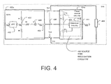
- FIG. 4 illustrates another embodiment of a system 400 consistent with the present invention.
- the system 400 may include an embodiment of a VOPS 102a and power control circuitry 104a consistent with the embodiments of FIGs. 1, 2, and 3A. For clarity, only those components of the VOPS 102a and the power control circuitry 104a related to detection of a particular type of VOPS are illustrated.
- the VOPS 102a and power control circuitry 104a may therefore include a host of other circuitry not illustrated.
- the power control circuitry 104a may include source type recognition circuitry 450.
- the interrogation signal sent by the source type recognition circuitry 450 may be a current signal.
- the source type recognition circuitry 450 may then evaluate a response to the current signal, e.g., a voltage level, to determine the type of VOPS 102a.
- the VOPS 102a may include a first resistor R1, a second resistor R2, and a third resistor R3 coupled to a feedback node 402.
- the VOPS 102a may be a variable output ACDC adapter in one embodiment.
- the VOPS 102a may also include voltage feedback circuitry (VFC) 412 which may also be coupled to the same feedback node 402.
- the voltage feedback circuitry 412 may receive an internal reference voltage Vref and a signal representative of an output voltage Vout of the VOPS 102a to control the output voltage Vout of the VOPS 102a.
- the VOPS 102a may further include a diode 408 coupled to the control path 406 to prevent reverse current flowing from the VOPS 102 to the power control circuitry 104a.
- the VOPS 102a may also include a control terminal 432 coupled to the control path 406.
- the power control circuitry 104a may include the source type recognition circuitry 450.
- the source type recognition circuitry 450 may include a fourth resistor R4 and detection circuitry 416.
- the fourth resistor R4 and the detection circuitry 416 may all be coupled to a control node 404.
- the control path 406 may couple the control terminal 432 of the VOPS 102a to the control node 404.
- the detection circuitry 416 may be configured to analyze a voltage level on the control terminal 432 and determine the type of the VOPS 102a in response to the voltage level.
- the value of the current extracted from the control node 404 may be set to vary from 0 to full current delivered through the fourth resistor R4.
- Ics I R4
- the VOPS 102a as controlled by the voltage feedback circuitry 412, will deliver the maximum output voltage given by equation (1).
- V out max ( 1 + R 1 / R 2 ) ⁇ V ref
- Voutmax is the maximum output voltage of the VOPS 102a
- R1 is a resistance value of the first resistor R1
- R2 is a resistance value of the second resistor R2
- Vref is the internal reference voltage provided to the voltage feedback circuitry 412.
- Voutmin is the minimum output voltage of the VOPS 102a
- R1 is a resistance value of the first resistor R1
- R2 is a resistance value of the second resistor R2
- R3 is a resistance value of the third resistor R3
- R4 is a resistance value of the fourth resistor R4
- Vref is the internal reference voltage provided to the voltage feedback circuitry 412.
- Vcs 432 The potential on the control terminal Vcs 432 may be approximated by equation (3).
- V C S ( R 3 / R 3 + R 4 ) ⁇ ( V out min ⁇ V ref )
- V CS is the potential at the control terminal 432
- R3 is the resistance value of the third resistor R3
- R4 is the resistance value of the fourth resistor R4
- Voutmin is the minimum output voltage of the VOPS 102a
- Vref is the internal reference voltage provided to the voltage feedback circuitry 412.
- variable output DC power sources belonging to the same class.
- the class may have the same internal reference voltage Vref and be targeted for the same Voutmax and Voutmin values.
- Vref internal reference voltage
- Voutmax the maximum output power rating
- load regulation load regulation
- line regulation line regulation
- over voltage/current protection features the maximum output voltage Voutmax as defined in equation (1) depends only the R1/R2 ratio if Vref is the same, each of the three types of variable output DC power sources may be designed with a different pair of first and second resistors R1 and R2.
- the first type of VOPS may be designed with a first and second resistor R1a, R2a
- the second type of VOPS may be designed with a first and second resistor R1b, R2b
- the third type of VOPS may be designed with a first and second resistor R1c, R2c provided that equation (4) is met.
- each type will have the same output voltage range while the potential on the control terminal Vcs 432 when the VOPS delivers Voutmin will have three different values V CSa , V CSb , V CSc that may be calculated by inserting the corresponding R3a, R3b, and R3c values of equations (7), (8), and (9) for R3 of equation (3).
- the detection circuitry 416 may be configured to analyze the voltage level at the control terminal 432 and compare the voltage level with particular values to determine the type of the VOPS in response to the particular voltage level.
- the detection circuitry 416 may include a number of voltage comparators for comparing the detected voltage level with differing preset voltage threshold levels and logic circuitry to detect and memorize the VOPS type. This and other circuitry known to those skilled in the art may be utilized in the detection circuitry 416.
- each of the three types of variable output DC power sources may have a different resistor sets for the first, second and third resistors (R1x, R2x, R3x) and consequently have a different impedance on the CS terminal 432 for each type.
- the same path 406 may be utilized to retrieve information about the VOPS type (V CSa , V CSb , V CSc ) and to send the interrogation signal.
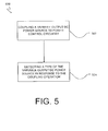
- FIG. 5 illustrates operations 500 according to an embodiment.
- Operation 502 may include coupling a variable output DC power source to power control circuitry.
- Operation 504 may include detecting a type of the variable output DC power source in response to the coupling operation.
- the detecting operation may include sending an interrogation signal from the power control circuitry to the variable output DC power source, and evaluating a response to the interrogation signal to determine the type of said variable output DC power source.
- power control circuitry may be utilized with different types of variable output DC power sources. After a variable output DC power source is coupled to the power control circuitry, the power control circuitry may be configured to detect which type is coupled to it. Therefore, one power control circuitry may be utilized with a number of different types of variable output DC power sources. The power control circuitry may automatically detect which type of variable output DC power source is coupled to it and may then control it accordingly. Hence, design flexibility may be increased and costs may be decreased.
Landscapes
- Engineering & Computer Science (AREA)
- Theoretical Computer Science (AREA)
- Power Engineering (AREA)
- Physics & Mathematics (AREA)
- General Engineering & Computer Science (AREA)
- General Physics & Mathematics (AREA)
- Dc-Dc Converters (AREA)
- Circuits Of Receivers In General (AREA)
- Selective Calling Equipment (AREA)
Applications Claiming Priority (2)
| Application Number | Priority Date | Filing Date | Title |
|---|---|---|---|
| US65071705P | 2005-02-07 | 2005-02-07 | |
| US11/113,532 US7777463B2 (en) | 2005-02-07 | 2005-04-25 | System, method and apparatus to automatically detect a type of a variable output DC power source |
Publications (2)
| Publication Number | Publication Date |
|---|---|
| EP1688824A1 true EP1688824A1 (de) | 2006-08-09 |
| EP1688824B1 EP1688824B1 (de) | 2010-03-31 |
Family
ID=36216288
Family Applications (1)
| Application Number | Title | Priority Date | Filing Date |
|---|---|---|---|
| EP05011428A Expired - Lifetime EP1688824B1 (de) | 2005-02-07 | 2005-05-27 | Leistungsregelungsschaltung zur Erkennung unterschiedlicher Arten von variablen Gleichstromsquellen |
Country Status (5)
| Country | Link |
|---|---|
| US (3) | US7777463B2 (de) |
| EP (1) | EP1688824B1 (de) |
| AT (1) | ATE463001T1 (de) |
| DE (1) | DE602005020244D1 (de) |
| TW (1) | TWI285746B (de) |
Cited By (1)
| Publication number | Priority date | Publication date | Assignee | Title |
|---|---|---|---|---|
| CN101726710B (zh) * | 2008-10-14 | 2011-12-14 | 和硕联合科技股份有限公司 | 电源测试控制装置、测试系统及其测试方法 |
Families Citing this family (3)
| Publication number | Priority date | Publication date | Assignee | Title |
|---|---|---|---|---|
| US7777463B2 (en) | 2005-02-07 | 2010-08-17 | O2Micro International Limited | System, method and apparatus to automatically detect a type of a variable output DC power source |
| US9325133B2 (en) | 2010-08-04 | 2016-04-26 | Hewlett-Packard Development Company, L.P. | Electrical adapter power rating determination |
| US20130159792A1 (en) * | 2011-01-24 | 2013-06-20 | Robert Brooks | Fault detection |
Citations (6)
| Publication number | Priority date | Publication date | Assignee | Title |
|---|---|---|---|---|
| US5298346A (en) * | 1992-07-27 | 1994-03-29 | Motorola, Inc. | Battery identification system |
| US5684382A (en) * | 1996-07-19 | 1997-11-04 | Compaq Computer Corporation | Control of computer AC adapter output voltage via battery pack feedback |
| US6175211B1 (en) * | 1999-04-15 | 2001-01-16 | Black & Decker Inc. | Battery pack with identification device |
| US20030025401A1 (en) * | 2001-08-01 | 2003-02-06 | Vlad Popescu-Stanesti | Intelligent adapter |
| US20030159073A1 (en) * | 2002-02-15 | 2003-08-21 | Breen John J. | Battery charger current limiting based on AC power adapter power |
| US6809649B1 (en) * | 1999-01-26 | 2004-10-26 | Telefonaktiebolaget Lm Ericsson(Publ) | Method and apparatus for communication between an electronic device and a connected battery |
Family Cites Families (12)
| Publication number | Priority date | Publication date | Assignee | Title |
|---|---|---|---|---|
| US6137279A (en) * | 1999-08-18 | 2000-10-24 | Sigmatel, Inc. | Adjustable power control module and applications thereof |
| DE19951944A1 (de) * | 1999-10-28 | 2001-05-03 | Mannesmann Rexroth Ag | Elektrische Schaltungsanordnung zur Umformung einer Eingangsspannung |
| JP3611100B2 (ja) * | 2000-02-29 | 2005-01-19 | シャープ株式会社 | 安定化電源回路および安定化電源用デバイス |
| US20020050812A1 (en) * | 2000-09-28 | 2002-05-02 | Michael Hoffman | Tri-range power supply system |
| US6507129B2 (en) * | 2001-03-12 | 2003-01-14 | Celestica International Inc. | System and method for controlling an output signal of a power supply |
| US6469478B1 (en) * | 2001-04-23 | 2002-10-22 | Artesyn Technologies, Inc. | Multiple output power supply including one regulated converter and at least one semi-regulated converter |
| US6975098B2 (en) * | 2002-01-31 | 2005-12-13 | Vlt, Inc. | Factorized power architecture with point of load sine amplitude converters |
| US6822426B1 (en) * | 2003-06-06 | 2004-11-23 | The Boeing Company | Regulator with feedback voltage and current signal summing into controller |
| US7243246B2 (en) * | 2003-12-19 | 2007-07-10 | Dell Products L.P. | System having a power adapter that generates a data signal based on the state of a external power source that is used to manage the power consumption of a CPU |
| US7453171B2 (en) * | 2004-01-15 | 2008-11-18 | Comarco Wireless Technologies, Inc | DC power source determination circuitry for use with an adapter |
| US7446503B2 (en) * | 2004-08-10 | 2008-11-04 | Illinois Tool Works Inc. | Method and apparatus for charging batteries using a converter |
| US7777463B2 (en) | 2005-02-07 | 2010-08-17 | O2Micro International Limited | System, method and apparatus to automatically detect a type of a variable output DC power source |
-
2005
- 2005-04-25 US US11/113,532 patent/US7777463B2/en not_active Expired - Lifetime
- 2005-05-27 EP EP05011428A patent/EP1688824B1/de not_active Expired - Lifetime
- 2005-05-27 AT AT05011428T patent/ATE463001T1/de not_active IP Right Cessation
- 2005-05-27 DE DE602005020244T patent/DE602005020244D1/de not_active Expired - Lifetime
-
2006
- 2006-01-18 TW TW095101940A patent/TWI285746B/zh not_active IP Right Cessation
-
2010
- 2010-08-17 US US12/857,661 patent/US8049471B2/en not_active Expired - Lifetime
-
2011
- 2011-10-31 US US13/285,684 patent/US8587264B2/en not_active Expired - Fee Related
Patent Citations (6)
| Publication number | Priority date | Publication date | Assignee | Title |
|---|---|---|---|---|
| US5298346A (en) * | 1992-07-27 | 1994-03-29 | Motorola, Inc. | Battery identification system |
| US5684382A (en) * | 1996-07-19 | 1997-11-04 | Compaq Computer Corporation | Control of computer AC adapter output voltage via battery pack feedback |
| US6809649B1 (en) * | 1999-01-26 | 2004-10-26 | Telefonaktiebolaget Lm Ericsson(Publ) | Method and apparatus for communication between an electronic device and a connected battery |
| US6175211B1 (en) * | 1999-04-15 | 2001-01-16 | Black & Decker Inc. | Battery pack with identification device |
| US20030025401A1 (en) * | 2001-08-01 | 2003-02-06 | Vlad Popescu-Stanesti | Intelligent adapter |
| US20030159073A1 (en) * | 2002-02-15 | 2003-08-21 | Breen John J. | Battery charger current limiting based on AC power adapter power |
Cited By (1)
| Publication number | Priority date | Publication date | Assignee | Title |
|---|---|---|---|---|
| CN101726710B (zh) * | 2008-10-14 | 2011-12-14 | 和硕联合科技股份有限公司 | 电源测试控制装置、测试系统及其测试方法 |
Also Published As
| Publication number | Publication date |
|---|---|
| US20060176632A1 (en) | 2006-08-10 |
| ATE463001T1 (de) | 2010-04-15 |
| US20120043948A1 (en) | 2012-02-23 |
| US8049471B2 (en) | 2011-11-01 |
| TWI285746B (en) | 2007-08-21 |
| US8587264B2 (en) | 2013-11-19 |
| EP1688824B1 (de) | 2010-03-31 |
| US7777463B2 (en) | 2010-08-17 |
| US20100308779A1 (en) | 2010-12-09 |
| TW200630631A (en) | 2006-09-01 |
| DE602005020244D1 (de) | 2010-05-12 |
Similar Documents
| Publication | Publication Date | Title |
|---|---|---|
| US8063514B2 (en) | Power supply selection/detection circuit | |
| US11360150B2 (en) | Fault detection for battery management systems | |
| KR101226374B1 (ko) | 전력 어댑터, 컴퓨터, 장치 및 매개 장치 | |
| US7917781B2 (en) | Universal USB power supply | |
| US7498783B2 (en) | Extending the continuous mode of operation for a buck converter | |
| US8111493B2 (en) | Current limit detector | |
| EP2383861A2 (de) | Batterieladegerät für tragbares elektronisches Gerät | |
| US20160357204A1 (en) | Power supply apparatus with cable voltage drop compensation | |
| EP2893608B1 (de) | Verfahren und system zum schutz vor spannungseinbruch | |
| US8732492B2 (en) | Information processing apparatus and method | |
| US8922218B2 (en) | Detection circuits for batteries | |
| US8587264B2 (en) | System, method and apparatus to automatically detect a type of a variable output DC power source | |
| CN115113284B (zh) | 异物侦测方法及具有异物侦测功能的电源端 | |
| CN1819431B (zh) | 用于自动检测可变输出直流电源的种类的功率控制电路 | |
| JP2951196B2 (ja) | バッテリ残量検出用電流検出装置 | |
| EP3458867B1 (de) | Beurteilung von antriebsmodi für mit gleichspannung versorgten vorrichtungen | |
| US12355291B2 (en) | Switching charger capable of accurately sensing small current | |
| US20130120008A1 (en) | Method of discrimination of a device as powerable through a lan line and device for estimating electric parameters of a lan line | |
| US8719596B2 (en) | Control, detection apparatus of power of network and detection method | |
| WO2007005047A2 (en) | System and method for configuring direct current converter | |
| KR101206124B1 (ko) | 배터리 잔량 측정 장치 및 그 방법 | |
| CN121689726A (zh) | 电源供应装置 | |
| BELL | Simple Charger Targets Lithium-Ion Batteries | |
| Munson | Four-quadrant power supply provides any-polarity voltage and current |
Legal Events
| Date | Code | Title | Description |
|---|---|---|---|
| PUAI | Public reference made under article 153(3) epc to a published international application that has entered the european phase |
Free format text: ORIGINAL CODE: 0009012 |
|
| AK | Designated contracting states |
Kind code of ref document: A1 Designated state(s): AT BE BG CH CY CZ DE DK EE ES FI FR GB GR HU IE IS IT LI LT LU MC NL PL PT RO SE SI SK TR |
|
| AX | Request for extension of the european patent |
Extension state: AL BA HR LV MK YU |
|
| 17P | Request for examination filed |
Effective date: 20070207 |
|
| AKX | Designation fees paid |
Designated state(s): AT BE BG CH CY CZ DE DK EE ES FI FR GB GR HU IE IS IT LI LT LU MC NL PL PT RO SE SI SK TR |
|
| 17Q | First examination report despatched |
Effective date: 20070425 |
|
| GRAP | Despatch of communication of intention to grant a patent |
Free format text: ORIGINAL CODE: EPIDOSNIGR1 |
|
| GRAS | Grant fee paid |
Free format text: ORIGINAL CODE: EPIDOSNIGR3 |
|
| GRAA | (expected) grant |
Free format text: ORIGINAL CODE: 0009210 |
|
| AK | Designated contracting states |
Kind code of ref document: B1 Designated state(s): AT BE BG CH CY CZ DE DK EE ES FI FR GB GR HU IE IS IT LI LT LU MC NL PL PT RO SE SI SK TR |
|
| REG | Reference to a national code |
Ref country code: CH Ref legal event code: EP Ref country code: GB Ref legal event code: FG4D |
|
| REG | Reference to a national code |
Ref country code: IE Ref legal event code: FG4D |
|
| REF | Corresponds to: |
Ref document number: 602005020244 Country of ref document: DE Date of ref document: 20100512 Kind code of ref document: P |
|
| REG | Reference to a national code |
Ref country code: NL Ref legal event code: VDEP Effective date: 20100331 |
|
| PG25 | Lapsed in a contracting state [announced via postgrant information from national office to epo] |
Ref country code: LT Free format text: LAPSE BECAUSE OF FAILURE TO SUBMIT A TRANSLATION OF THE DESCRIPTION OR TO PAY THE FEE WITHIN THE PRESCRIBED TIME-LIMIT Effective date: 20100331 |
|
| LTIE | Lt: invalidation of european patent or patent extension |
Effective date: 20100331 |
|
| PG25 | Lapsed in a contracting state [announced via postgrant information from national office to epo] |
Ref country code: SI Free format text: LAPSE BECAUSE OF FAILURE TO SUBMIT A TRANSLATION OF THE DESCRIPTION OR TO PAY THE FEE WITHIN THE PRESCRIBED TIME-LIMIT Effective date: 20100331 Ref country code: PL Free format text: LAPSE BECAUSE OF FAILURE TO SUBMIT A TRANSLATION OF THE DESCRIPTION OR TO PAY THE FEE WITHIN THE PRESCRIBED TIME-LIMIT Effective date: 20100331 Ref country code: FI Free format text: LAPSE BECAUSE OF FAILURE TO SUBMIT A TRANSLATION OF THE DESCRIPTION OR TO PAY THE FEE WITHIN THE PRESCRIBED TIME-LIMIT Effective date: 20100331 Ref country code: AT Free format text: LAPSE BECAUSE OF FAILURE TO SUBMIT A TRANSLATION OF THE DESCRIPTION OR TO PAY THE FEE WITHIN THE PRESCRIBED TIME-LIMIT Effective date: 20100331 |
|
| PG25 | Lapsed in a contracting state [announced via postgrant information from national office to epo] |
Ref country code: SE Free format text: LAPSE BECAUSE OF FAILURE TO SUBMIT A TRANSLATION OF THE DESCRIPTION OR TO PAY THE FEE WITHIN THE PRESCRIBED TIME-LIMIT Effective date: 20100331 Ref country code: RO Free format text: LAPSE BECAUSE OF FAILURE TO SUBMIT A TRANSLATION OF THE DESCRIPTION OR TO PAY THE FEE WITHIN THE PRESCRIBED TIME-LIMIT Effective date: 20100331 Ref country code: NL Free format text: LAPSE BECAUSE OF FAILURE TO SUBMIT A TRANSLATION OF THE DESCRIPTION OR TO PAY THE FEE WITHIN THE PRESCRIBED TIME-LIMIT Effective date: 20100331 Ref country code: ES Free format text: LAPSE BECAUSE OF FAILURE TO SUBMIT A TRANSLATION OF THE DESCRIPTION OR TO PAY THE FEE WITHIN THE PRESCRIBED TIME-LIMIT Effective date: 20100712 Ref country code: EE Free format text: LAPSE BECAUSE OF FAILURE TO SUBMIT A TRANSLATION OF THE DESCRIPTION OR TO PAY THE FEE WITHIN THE PRESCRIBED TIME-LIMIT Effective date: 20100331 Ref country code: BE Free format text: LAPSE BECAUSE OF FAILURE TO SUBMIT A TRANSLATION OF THE DESCRIPTION OR TO PAY THE FEE WITHIN THE PRESCRIBED TIME-LIMIT Effective date: 20100331 Ref country code: CY Free format text: LAPSE BECAUSE OF FAILURE TO SUBMIT A TRANSLATION OF THE DESCRIPTION OR TO PAY THE FEE WITHIN THE PRESCRIBED TIME-LIMIT Effective date: 20100331 |
|
| PG25 | Lapsed in a contracting state [announced via postgrant information from national office to epo] |
Ref country code: CZ Free format text: LAPSE BECAUSE OF FAILURE TO SUBMIT A TRANSLATION OF THE DESCRIPTION OR TO PAY THE FEE WITHIN THE PRESCRIBED TIME-LIMIT Effective date: 20100331 Ref country code: SK Free format text: LAPSE BECAUSE OF FAILURE TO SUBMIT A TRANSLATION OF THE DESCRIPTION OR TO PAY THE FEE WITHIN THE PRESCRIBED TIME-LIMIT Effective date: 20100331 Ref country code: IS Free format text: LAPSE BECAUSE OF FAILURE TO SUBMIT A TRANSLATION OF THE DESCRIPTION OR TO PAY THE FEE WITHIN THE PRESCRIBED TIME-LIMIT Effective date: 20100731 |
|
| PG25 | Lapsed in a contracting state [announced via postgrant information from national office to epo] |
Ref country code: MC Free format text: LAPSE BECAUSE OF NON-PAYMENT OF DUE FEES Effective date: 20100531 |
|
| REG | Reference to a national code |
Ref country code: CH Ref legal event code: PL |
|
| PG25 | Lapsed in a contracting state [announced via postgrant information from national office to epo] |
Ref country code: PT Free format text: LAPSE BECAUSE OF FAILURE TO SUBMIT A TRANSLATION OF THE DESCRIPTION OR TO PAY THE FEE WITHIN THE PRESCRIBED TIME-LIMIT Effective date: 20100802 Ref country code: DK Free format text: LAPSE BECAUSE OF FAILURE TO SUBMIT A TRANSLATION OF THE DESCRIPTION OR TO PAY THE FEE WITHIN THE PRESCRIBED TIME-LIMIT Effective date: 20100331 |
|
| PLBE | No opposition filed within time limit |
Free format text: ORIGINAL CODE: 0009261 |
|
| STAA | Information on the status of an ep patent application or granted ep patent |
Free format text: STATUS: NO OPPOSITION FILED WITHIN TIME LIMIT |
|
| PG25 | Lapsed in a contracting state [announced via postgrant information from national office to epo] |
Ref country code: CH Free format text: LAPSE BECAUSE OF NON-PAYMENT OF DUE FEES Effective date: 20100531 Ref country code: LI Free format text: LAPSE BECAUSE OF NON-PAYMENT OF DUE FEES Effective date: 20100531 |
|
| 26N | No opposition filed |
Effective date: 20110104 |
|
| PG25 | Lapsed in a contracting state [announced via postgrant information from national office to epo] |
Ref country code: IE Free format text: LAPSE BECAUSE OF NON-PAYMENT OF DUE FEES Effective date: 20100527 |
|
| PG25 | Lapsed in a contracting state [announced via postgrant information from national office to epo] |
Ref country code: LU Free format text: LAPSE BECAUSE OF NON-PAYMENT OF DUE FEES Effective date: 20100527 Ref country code: HU Free format text: LAPSE BECAUSE OF FAILURE TO SUBMIT A TRANSLATION OF THE DESCRIPTION OR TO PAY THE FEE WITHIN THE PRESCRIBED TIME-LIMIT Effective date: 20101001 Ref country code: BG Free format text: LAPSE BECAUSE OF FAILURE TO SUBMIT A TRANSLATION OF THE DESCRIPTION OR TO PAY THE FEE WITHIN THE PRESCRIBED TIME-LIMIT Effective date: 20100331 |
|
| PG25 | Lapsed in a contracting state [announced via postgrant information from national office to epo] |
Ref country code: TR Free format text: LAPSE BECAUSE OF FAILURE TO SUBMIT A TRANSLATION OF THE DESCRIPTION OR TO PAY THE FEE WITHIN THE PRESCRIBED TIME-LIMIT Effective date: 20100331 |
|
| PG25 | Lapsed in a contracting state [announced via postgrant information from national office to epo] |
Ref country code: BG Free format text: LAPSE BECAUSE OF FAILURE TO SUBMIT A TRANSLATION OF THE DESCRIPTION OR TO PAY THE FEE WITHIN THE PRESCRIBED TIME-LIMIT Effective date: 20100630 |
|
| PG25 | Lapsed in a contracting state [announced via postgrant information from national office to epo] |
Ref country code: GR Free format text: LAPSE BECAUSE OF FAILURE TO SUBMIT A TRANSLATION OF THE DESCRIPTION OR TO PAY THE FEE WITHIN THE PRESCRIBED TIME-LIMIT Effective date: 20100331 |
|
| REG | Reference to a national code |
Ref country code: FR Ref legal event code: PLFP Year of fee payment: 11 |
|
| PGFP | Annual fee paid to national office [announced via postgrant information from national office to epo] |
Ref country code: GB Payment date: 20150527 Year of fee payment: 11 Ref country code: DE Payment date: 20150528 Year of fee payment: 11 |
|
| PGFP | Annual fee paid to national office [announced via postgrant information from national office to epo] |
Ref country code: FR Payment date: 20150519 Year of fee payment: 11 Ref country code: IT Payment date: 20150527 Year of fee payment: 11 |
|
| REG | Reference to a national code |
Ref country code: DE Ref legal event code: R119 Ref document number: 602005020244 Country of ref document: DE |
|
| GBPC | Gb: european patent ceased through non-payment of renewal fee |
Effective date: 20160527 |
|
| PG25 | Lapsed in a contracting state [announced via postgrant information from national office to epo] |
Ref country code: IT Free format text: LAPSE BECAUSE OF NON-PAYMENT OF DUE FEES Effective date: 20160527 |
|
| REG | Reference to a national code |
Ref country code: FR Ref legal event code: ST Effective date: 20170131 |
|
| PG25 | Lapsed in a contracting state [announced via postgrant information from national office to epo] |
Ref country code: DE Free format text: LAPSE BECAUSE OF NON-PAYMENT OF DUE FEES Effective date: 20161201 Ref country code: FR Free format text: LAPSE BECAUSE OF NON-PAYMENT OF DUE FEES Effective date: 20160531 |
|
| PG25 | Lapsed in a contracting state [announced via postgrant information from national office to epo] |
Ref country code: GB Free format text: LAPSE BECAUSE OF NON-PAYMENT OF DUE FEES Effective date: 20160527 |