EP1696253A2 - Präzise relative Ausrichtung und epoxidfreie Befestigung optischer Elemente - Google Patents
Präzise relative Ausrichtung und epoxidfreie Befestigung optischer Elemente Download PDFInfo
- Publication number
- EP1696253A2 EP1696253A2 EP06075246A EP06075246A EP1696253A2 EP 1696253 A2 EP1696253 A2 EP 1696253A2 EP 06075246 A EP06075246 A EP 06075246A EP 06075246 A EP06075246 A EP 06075246A EP 1696253 A2 EP1696253 A2 EP 1696253A2
- Authority
- EP
- European Patent Office
- Prior art keywords
- substrate
- layer
- solder
- metal
- solder bumps
- Prior art date
- Legal status (The legal status is an assumption and is not a legal conclusion. Google has not performed a legal analysis and makes no representation as to the accuracy of the status listed.)
- Withdrawn
Links
Images


Classifications
-
- H—ELECTRICITY
- H05—ELECTRIC TECHNIQUES NOT OTHERWISE PROVIDED FOR
- H05K—PRINTED CIRCUITS; CASINGS OR CONSTRUCTIONAL DETAILS OF ELECTRIC APPARATUS; MANUFACTURE OF ASSEMBLAGES OF ELECTRICAL COMPONENTS
- H05K3/00—Apparatus or processes for manufacturing printed circuits
- H05K3/30—Assembling printed circuits with electric components, e.g. with resistors
- H05K3/32—Assembling printed circuits with electric components, e.g. with resistors electrically connecting electric components or wires to printed circuits
- H05K3/34—Assembling printed circuits with electric components, e.g. with resistors electrically connecting electric components or wires to printed circuits by soldering
- H05K3/341—Surface mounted components
- H05K3/3431—Leadless components
- H05K3/3436—Leadless components having an array of bottom contacts, e.g. pad grid array or ball grid array components
-
- B—PERFORMING OPERATIONS; TRANSPORTING
- B23—MACHINE TOOLS; METAL-WORKING NOT OTHERWISE PROVIDED FOR
- B23K—SOLDERING OR UNSOLDERING; WELDING; CLADDING OR PLATING BY SOLDERING OR WELDING; CUTTING BY APPLYING HEAT LOCALLY, e.g. FLAME CUTTING; WORKING BY LASER BEAM
- B23K3/00—Tools, devices or special appurtenances for soldering, e.g. brazing, or unsoldering, not specially adapted for particular methods
- B23K3/06—Solder feeding devices; Solder melting pans
- B23K3/0607—Solder feeding devices
- B23K3/0623—Solder feeding devices for shaped solder piece feeding, e.g. preforms, bumps, balls, pellets, droplets
-
- G—PHYSICS
- G02—OPTICS
- G02B—OPTICAL ELEMENTS, SYSTEMS OR APPARATUS
- G02B27/00—Optical systems or apparatus not provided for by any of the groups G02B1/00 - G02B26/00, G02B30/00
- G02B27/62—Optical apparatus specially adapted for adjusting optical elements during the assembly of optical systems
-
- B—PERFORMING OPERATIONS; TRANSPORTING
- B23—MACHINE TOOLS; METAL-WORKING NOT OTHERWISE PROVIDED FOR
- B23K—SOLDERING OR UNSOLDERING; WELDING; CLADDING OR PLATING BY SOLDERING OR WELDING; CUTTING BY APPLYING HEAT LOCALLY, e.g. FLAME CUTTING; WORKING BY LASER BEAM
- B23K2101/00—Articles made by soldering, welding or cutting
- B23K2101/36—Electric or electronic devices
- B23K2101/42—Printed circuits
-
- G—PHYSICS
- G02—OPTICS
- G02B—OPTICAL ELEMENTS, SYSTEMS OR APPARATUS
- G02B6/00—Light guides; Structural details of arrangements comprising light guides and other optical elements, e.g. couplings
- G02B6/24—Coupling light guides
- G02B6/42—Coupling light guides with opto-electronic elements
- G02B6/4201—Packages, e.g. shape, construction, internal or external details
- G02B6/4219—Mechanical fixtures for holding or positioning the elements relative to each other in the couplings; Alignment methods for the elements, e.g. measuring or observing methods especially used therefor
- G02B6/4228—Passive alignment, i.e. without a detection of the degree of coupling or the position of the elements
- G02B6/4232—Passive alignment, i.e. without a detection of the degree of coupling or the position of the elements using the surface tension of fluid solder to align the elements, e.g. solder bump techniques
-
- H—ELECTRICITY
- H05—ELECTRIC TECHNIQUES NOT OTHERWISE PROVIDED FOR
- H05K—PRINTED CIRCUITS; CASINGS OR CONSTRUCTIONAL DETAILS OF ELECTRIC APPARATUS; MANUFACTURE OF ASSEMBLAGES OF ELECTRICAL COMPONENTS
- H05K2203/00—Indexing scheme relating to apparatus or processes for manufacturing printed circuits covered by H05K3/00
- H05K2203/04—Soldering or other types of metallurgic bonding
- H05K2203/048—Self-alignment during soldering; Terminals, pads or shape of solder adapted therefor
-
- H—ELECTRICITY
- H10—SEMICONDUCTOR DEVICES; ELECTRIC SOLID-STATE DEVICES NOT OTHERWISE PROVIDED FOR
- H10W—GENERIC PACKAGES, INTERCONNECTIONS, CONNECTORS OR OTHER CONSTRUCTIONAL DETAILS OF DEVICES COVERED BY CLASS H10
- H10W72/00—Interconnections or connectors in packages
- H10W72/01—Manufacture or treatment
- H10W72/012—Manufacture or treatment of bump connectors, dummy bumps or thermal bumps
- H10W72/01231—Manufacture or treatment of bump connectors, dummy bumps or thermal bumps using blanket deposition
-
- H—ELECTRICITY
- H10—SEMICONDUCTOR DEVICES; ELECTRIC SOLID-STATE DEVICES NOT OTHERWISE PROVIDED FOR
- H10W—GENERIC PACKAGES, INTERCONNECTIONS, CONNECTORS OR OTHER CONSTRUCTIONAL DETAILS OF DEVICES COVERED BY CLASS H10
- H10W72/00—Interconnections or connectors in packages
- H10W72/01—Manufacture or treatment
- H10W72/012—Manufacture or treatment of bump connectors, dummy bumps or thermal bumps
- H10W72/01251—Changing the shapes of bumps
- H10W72/01255—Changing the shapes of bumps by using masks
-
- H—ELECTRICITY
- H10—SEMICONDUCTOR DEVICES; ELECTRIC SOLID-STATE DEVICES NOT OTHERWISE PROVIDED FOR
- H10W—GENERIC PACKAGES, INTERCONNECTIONS, CONNECTORS OR OTHER CONSTRUCTIONAL DETAILS OF DEVICES COVERED BY CLASS H10
- H10W72/00—Interconnections or connectors in packages
- H10W72/01—Manufacture or treatment
- H10W72/016—Manufacture or treatment of strap connectors
-
- H—ELECTRICITY
- H10—SEMICONDUCTOR DEVICES; ELECTRIC SOLID-STATE DEVICES NOT OTHERWISE PROVIDED FOR
- H10W—GENERIC PACKAGES, INTERCONNECTIONS, CONNECTORS OR OTHER CONSTRUCTIONAL DETAILS OF DEVICES COVERED BY CLASS H10
- H10W72/00—Interconnections or connectors in packages
- H10W72/01—Manufacture or treatment
- H10W72/019—Manufacture or treatment of bond pads
-
- H—ELECTRICITY
- H10—SEMICONDUCTOR DEVICES; ELECTRIC SOLID-STATE DEVICES NOT OTHERWISE PROVIDED FOR
- H10W—GENERIC PACKAGES, INTERCONNECTIONS, CONNECTORS OR OTHER CONSTRUCTIONAL DETAILS OF DEVICES COVERED BY CLASS H10
- H10W72/00—Interconnections or connectors in packages
- H10W72/071—Connecting or disconnecting
- H10W72/072—Connecting or disconnecting of bump connectors
- H10W72/07221—Aligning
-
- H—ELECTRICITY
- H10—SEMICONDUCTOR DEVICES; ELECTRIC SOLID-STATE DEVICES NOT OTHERWISE PROVIDED FOR
- H10W—GENERIC PACKAGES, INTERCONNECTIONS, CONNECTORS OR OTHER CONSTRUCTIONAL DETAILS OF DEVICES COVERED BY CLASS H10
- H10W72/00—Interconnections or connectors in packages
- H10W72/071—Connecting or disconnecting
- H10W72/072—Connecting or disconnecting of bump connectors
- H10W72/07231—Techniques
- H10W72/07234—Using a reflow oven
-
- H—ELECTRICITY
- H10—SEMICONDUCTOR DEVICES; ELECTRIC SOLID-STATE DEVICES NOT OTHERWISE PROVIDED FOR
- H10W—GENERIC PACKAGES, INTERCONNECTIONS, CONNECTORS OR OTHER CONSTRUCTIONAL DETAILS OF DEVICES COVERED BY CLASS H10
- H10W72/00—Interconnections or connectors in packages
- H10W72/071—Connecting or disconnecting
- H10W72/072—Connecting or disconnecting of bump connectors
- H10W72/07231—Techniques
- H10W72/07236—Soldering or alloying
-
- H—ELECTRICITY
- H10—SEMICONDUCTOR DEVICES; ELECTRIC SOLID-STATE DEVICES NOT OTHERWISE PROVIDED FOR
- H10W—GENERIC PACKAGES, INTERCONNECTIONS, CONNECTORS OR OTHER CONSTRUCTIONAL DETAILS OF DEVICES COVERED BY CLASS H10
- H10W72/00—Interconnections or connectors in packages
- H10W72/071—Connecting or disconnecting
- H10W72/072—Connecting or disconnecting of bump connectors
- H10W72/07251—Connecting or disconnecting of bump connectors characterised by changes in properties of the bump connectors during connecting
-
- H—ELECTRICITY
- H10—SEMICONDUCTOR DEVICES; ELECTRIC SOLID-STATE DEVICES NOT OTHERWISE PROVIDED FOR
- H10W—GENERIC PACKAGES, INTERCONNECTIONS, CONNECTORS OR OTHER CONSTRUCTIONAL DETAILS OF DEVICES COVERED BY CLASS H10
- H10W72/00—Interconnections or connectors in packages
- H10W72/20—Bump connectors, e.g. solder bumps or copper pillars; Dummy bumps; Thermal bumps
- H10W72/251—Materials
- H10W72/252—Materials comprising solid metals or solid metalloids, e.g. PbSn, Ag or Cu
-
- H—ELECTRICITY
- H10—SEMICONDUCTOR DEVICES; ELECTRIC SOLID-STATE DEVICES NOT OTHERWISE PROVIDED FOR
- H10W—GENERIC PACKAGES, INTERCONNECTIONS, CONNECTORS OR OTHER CONSTRUCTIONAL DETAILS OF DEVICES COVERED BY CLASS H10
- H10W72/00—Interconnections or connectors in packages
- H10W72/90—Bond pads, in general
- H10W72/921—Structures or relative sizes of bond pads
- H10W72/923—Bond pads having multiple stacked layers
-
- H—ELECTRICITY
- H10—SEMICONDUCTOR DEVICES; ELECTRIC SOLID-STATE DEVICES NOT OTHERWISE PROVIDED FOR
- H10W—GENERIC PACKAGES, INTERCONNECTIONS, CONNECTORS OR OTHER CONSTRUCTIONAL DETAILS OF DEVICES COVERED BY CLASS H10
- H10W72/00—Interconnections or connectors in packages
- H10W72/90—Bond pads, in general
- H10W72/941—Dispositions of bond pads
- H10W72/9415—Dispositions of bond pads relative to the surface, e.g. recessed, protruding
-
- H—ELECTRICITY
- H10—SEMICONDUCTOR DEVICES; ELECTRIC SOLID-STATE DEVICES NOT OTHERWISE PROVIDED FOR
- H10W—GENERIC PACKAGES, INTERCONNECTIONS, CONNECTORS OR OTHER CONSTRUCTIONAL DETAILS OF DEVICES COVERED BY CLASS H10
- H10W72/00—Interconnections or connectors in packages
- H10W72/90—Bond pads, in general
- H10W72/951—Materials of bond pads
- H10W72/952—Materials of bond pads comprising metals or metalloids, e.g. PbSn, Ag or Cu
-
- Y—GENERAL TAGGING OF NEW TECHNOLOGICAL DEVELOPMENTS; GENERAL TAGGING OF CROSS-SECTIONAL TECHNOLOGIES SPANNING OVER SEVERAL SECTIONS OF THE IPC; TECHNICAL SUBJECTS COVERED BY FORMER USPC CROSS-REFERENCE ART COLLECTIONS [XRACs] AND DIGESTS
- Y02—TECHNOLOGIES OR APPLICATIONS FOR MITIGATION OR ADAPTATION AGAINST CLIMATE CHANGE
- Y02P—CLIMATE CHANGE MITIGATION TECHNOLOGIES IN THE PRODUCTION OR PROCESSING OF GOODS
- Y02P70/00—Climate change mitigation technologies in the production process for final industrial or consumer products
- Y02P70/50—Manufacturing or production processes characterised by the final manufactured product
Definitions
- This invention relates generally to techniques for affixing and aligning components on a common substrate and, more particularly, to techniques for accurate alignment of optical components on a common substrate.
- Fabrication, of optoelectronic modules presents a significantly greater challenge than fabrication of semiconductor modules, the fundamental difference being the need to achieve and maintain a high accuracy in alignment between optical and optoelectronic components.
- Optical adhesives were originally two-part epoxies formulated to optimize their properties of adhesion and strength. These materials have been further refined for use in applications involving precise alignment, positioning and centering applications. Use of adhesives in such applications has been facilitated by the cure-on-demand characteristic of ultraviolet (UV) curable materials.
- UV curable materials Such adhesives, however, are not suitable for bonding components in hermetic packages containing laser diodes. This is because laser diodes are subject to a mechanism of catastrophic optical damage (COD) in which organic compounds contained in the adhesive contaminate the emitting facet of the diode, ultimately leading to failure. Solders requiring flux lead to the same mechanism of COD as organic adhesives, and therefore should also be avoided in the packaging of devices that include laser diodes.
- COD catastrophic optical damage
- the present invention resides in a novel process for accurate alignment and attachment of components on a common substrate, using a fluxless, self-aligning bump-bonding technique.
- the method of the invention may be defined as including the steps of applying to a surface of each component to be attached to the substrate, a plurality of metal pads, the plurality of pads being arranged in a selected pattern; applying to a surface of the substrate, a plurality of patterns of solder bumps, each pattern of solder bumps being congruent with a corresponding pattern of metal pads on a component.
- the succeeding steps of the method include placing each component on the substrate with the pattern of metal pads on the component in near-congruence with the corresponding pattern on the substrate; then heating the substrate and the components and thereby reflowing the solder bumps. As a result of reflowing the solder bumps, each component is automatically aligned on the substrate. Each component is allowed to move laterally and rotationally to align the corresponding patterns of solder bumps and metal pads. Upon cooling of the substrate and the components, the solder bumps return to the solid state, and the components remain accurately aligned in their desired positions on the substrate.
- the pattern of metal pads on the component and the corresponding pattern of solder bumps on the substrate each include a distinctively shaped pad and solder bump, respectively.
- each pattern may include one pad (or bump) of square cross section, as easily distinguished from the other pads and bumps of circular cross section.
- the step of applying solder bumps to the substrate comprises applying a photoresist layer to the substrate; photolithographically patterning the photoresist layer to form in the layer openings that define the pattern of solder bumps in position and dimensions; depositing solder on the substrate, to form the solder bumps on the substrate; and then removing the photoresist layer.
- the step of applying solder bumps to the substrate may further comprise the steps of applying a metal layer to the substrate before applying the photoresist layer; and later removing portions of the metal layer not contained beneath the solder bumps, after the photoresist layer has been removed.
- the metal serves as an adhesion layer for the solder.
- the solder is a gold-tin (Au-Sn) solder in the ratio 80/20 and the substrate is of copper-tungsten (CuW).
- the metal layer is nickel (Ni) and the metal layer is later removed by chemical etching.
- the step of applying a plurality of metal pads to each component comprises forming multiple successive metal layers on the component; lithographically patterning the metal layers; and then removing unwanted materials from the structure.
- the multiple metal layers are applied first, then patterned with a photoresist layer to define the desired metal pads.
- the removing step includes etching away the unwanted portions of the metal layer and removing the photoresist layer.
- the patterning step is performed first, to define pad areas by openings in a photoresist layer; and the step of forming successive metal layers applies metal through the openings in the photoresist layer.
- the removing step removes the photoresist layer, to leave the metal pads in the desired pattern.
- each pattern further comprises at least one reference line corresponding with a geometric feature of the component.
- the photolithographic pattern includes a pair of lines at right-angies, corresponding to the position of a right-angle edge of the component, such as a right-angle prism.
- the step of forming multiple successive metal layers on a glass component comprises the steps of, first, applying a titanium layer to serve as an adhesion layer for a component of glass; next applying a Ni layer over the titanium, to serve as a diffusion barrier; and then applying a gold layer over the Ni layer, to serve as a wetting layer for the solder.
- the present invention represents a significant advance in the field of accurate affixing and alignment of components, such as optical components on a common substrate.
- the invention results in accurate positioning and alignment of components without the need for real-time alignment steps and without using optical adhesives or solder requiring flux.
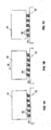
- FIGS. 1A-1C together depict the phenomenon of self-alignment employed in the method of the present invention.
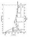
- FIG. 2 is a gold-tin equilibrium phase diagram.
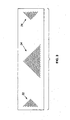
- FIG. 3 is a schematic view of a submount bumping pattern.
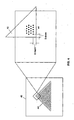
- FIG. 4 is a schematic view of an optical component alignment pattern and a depiction of how that pattern is aligned with respect to a component (prism).
- FIGS. 5A-5D together show a process for forming a pattern of solder bumps on a submount.
- FIGS. 6A-6D together show a process for forming a pattern of solder pads on a submount or substrate.
- FIGS. 7A-7C together show an alternate process for forming a pattern of solder pads on a submount.
- FIG. 8 is a schematic view of a bumping pattern for an optical component, and also showing a pair of right-angle lines used for alignment of the pattern on a component (prism).
- the present invention is concerned with methods for affixing and aligning components with great accuracy on a common substrate.
- alignment was achieved only by means of real-time active measurement during attachment using an organic adhesive.
- components such as optical prisms
- a self-aligning soldering technique can be implemented by the deposition of solder bumps on the substrate and pads on each component. Active measurement during assembly is not required because component alignment is guaranteed within the geometry of the bump spacing or pitch, and is further guaranteed through a self-alignment phenomenon that arises from the tendency of molten solder to form a shape that minimizes surface energy and therefore surface area.
- FIGS. 1A, 1B and 1C together depict in diagrammatic form the self-alignment phenomenon that is a critical aspect of the present invention.
- an optical component 10 shown as a prism by way of example, is initially placed over a submount 12 with some degree of misalignment.
- the terms "submount” and “substrate” are used synonymously.
- the submount 12 has formed on its upper surface a pattern of solder bumps 14.
- the prism 10 has on its underside an identically spaced pattern of solder pads 16. It will be understood, however, that for some applications of the invention the locations of the solder bumps 14 and solder pads 16 may be reversed.
- this misalignment is shown as being along an axis parallel to the planar interface between the prism 10 and submount 12.
- the misalignment may be in either or both of two orthogonal directions (x and y) in this planar interface, and may also include a rotational misalignment about a third axis '(z) perpendicular to the x and y axes.
- FIG. 1B illustrates the same structure as FIG. 1A but at the beginning of a solder reflow step, in which the solder bumps 14 are heated sufflciently for the solder to enter the liquid phase. Because of the tendency of each of the solder bumps 14 to minimize its surface area, the bumps assume a near spherical in shape, and in doing so apply an alignment force on the solder pads 16, as indicated by the arrow 18. For the solder bumps 14 to reach a symmetrical near-spherical form, the solder pads 16, and with them the prism 10, are translated laterally to the fully aligned position shown in FIG. 1C. It will be understood that, depending on the nature of the initial misalignment, the reflow step may also result in a component of alignment force along the other of the x and y axes and, if necessary, a rotational self-alignment torque.
- bonding is effected using eutectic Au-Sn (80/20) metallurgy.
- This system is desirable for use in a photonics package because it offers the advantages of good mechanical properties, low melting temperature, and fluxless reflow, which precludes contamination of optically active surfaces.
- the Au-Sn equilibrium phase diagram is shown in FIG. 2. It shows that there are six intermetallic phases, four of which are stable at ambient conditions, and the two solid solutions.
- the solder alloy at 20 wt% Sn is chosen for its eutectic composition, which, upon cooling the molten alloy through the eutectic temperature of 278 °C, solidifies to form a eutectic structure of the Au 5 Sn and AuSn phases.
- Au-Sn metallurgy can be found in a paper by Song, H.G., Ahn, J.P., and Morris, Jr., J.W., "The microstructure of eutectic Au-Sn solder bumps on Cu/ electroless Ni/Au", J. of Electronic Materials, 30 [9] 2001.
- FIG. 3 depicts a pattern 20 for a submount 12, with three alignment patterns 22, 24 and 26 formed as part of it.
- the three submount alignment patterns 22, 24 and 26 are all formed as a single pattern 20 that accurately reflects the positioning and alignment of the three components.
- the component alignment pattern 40 includes pairs of lines at right angles to each other 44, or at some other angle if the prisms being mounted and aligned are not right prisms. As described below with reference to FIG.
- these right-angle lines facilitate the placement of the alignment pattern on the prism, and therefore the alignment of the prisms on the submount.
- the off-set of these pairs of lines from the component alignment pattern creates congruency between the submount alignment pattern, the component alignment pattern, and the desired feature of the component to be aligned, such as the reflecting surface of a prism.
- FIG. 4 depicts a critical alignment step in forming a' pattern on a component such as a prism 10.
- a prism alignment pattern 40 is formed to define a triangular array that will be used to define the positions of solder pads, and a pair of lines 44 at right-angles to each other. As indicated in the figure, prior to forming the solder pads on the prism 10, the pattern 40 is aligned over the prism such that the roof angle of the prism is aligned with the pair of lines 44. Then the process of forming the solder pads is performed, as described in more detail below.
- FIGS. 5A-5D Processing of the submount 12 to form a pattern of solder bumps 14 on its surface is depicted in FIGS. 5A-5D.
- a layer of Ni 50 is first applied to the submount 12, which, in the preferred embodiment of the invention is of a copper-tungsten (CuW) alloy.
- the Ni layer 50 may be conveniently formed by electroplating, with a thickness of approximately 2.5 ⁇ m.
- the Ni layer 50 serves as an adhesion layer and forms the under-bump metallurgy (UBM) for the later applied (Au-Sn) solder.
- UBM under-bump metallurgy
- the Ni barrier layer 50 results in formation of an intermetallic interface of Ni 3 Sn 2 that forms the connection between the solder and Ni.
- the growth of this layer has been studied and found to be relatively slow, following a rate proportional to the square root of time, suggesting its diffusion-limited growth. Furthermore, growth of this phase has not been found to decrease the strength of the resulting joints.
- the electroplated parts are masked by applying a photoresist layer 52 that is subsequently structured in a photolithographic step, which defines the positions of the solder bumps as openings in the photoresist layer 52.
- the negatively masked sub-mounts are then electroplated with approximately 30 ⁇ m of solder alloy, (80/20 Au-Sn), as indicated at 54 in FIG. 5C.
- the photomask 52 is subsequently removed by an acetone soak, revealing the desired array of solder bumps 14, as depicted in FIG. 5D.
- the electroplated Ni layer 50 is removed by means of a chemical etch (FeCl 3 ), revealing the original CuW surface between the solder bumps 14. This step is taken to ensure a non-wetting condition between the solder bumps 14 and substrate.
- the composition and thickness of the evaporated bumps are confirmed by energy dispersive spectroscopy (EDS) and profilometry, respectively.
- FIGS. 6A-6D show the processing steps used to form a pattern of solder pads 16 on an optical component 10, such as a prism.
- the solder pads 16 were developed on prisms of BK7 glass, which has a comparable coefficient of thermal expansion to the CuW material chosen for the submount 12.
- the pad metallurgy consists of a first layer (200 nm thick) of titanium (Ti), followed by a second layer (1000 nm thick) of Ni, and a third layer (300 nm) of Au.
- These layers indicated collectively by reference numeral 60, are deposited on the prism 10 using a single gun four-source electron-beam deposition (EBD) system.
- ESD electron-beam deposition
- the Ti serves as an adhesion layer to the glass
- the Ni provides a diffusion barrier
- Au serves as a wetting layer for the solder. Deleterious effects of oxidation of the metal surfaces can be minimized by keeping the samples in the evaporation chamber between depositions of the various layers, and minimizing the intervening times.
- a photolithographic step as indicated in FIG. 6B, a resist layer 62 is applied over the evaporated metal layers 60 and is patterned to define the positions of the solder pads 16.
- the exposed Au, Ni, and Ti layers 60 are removed through a three-stage chemical etch with aqueous solutions of K+Kl, FeCl 3 , and HF/HNO 3 respectively.
- the remaining portions of the photoresist 62 are finally removed with an acetone soak, revealing a corresponding array of pads 16 to the solder bumps developed on the sub-mounts.
- FIGS. 7A-7C illustrate an alternative to the pattern etching process of FIGS. 6A-6D.
- the photolithography step and the evaporation steps are reversed.
- FIG. 7A shows an initial photolithography step, in which a resist layer 62' is first formed, then patterned to leave openings that defined the positions of the solder pads 16.
- FIG. 7B shows the layers of Ti, Ni and Au are evaporated into the regions exposed by the photolithography step of FIG. 7A.
- the resist layer 60' is removed by a lift-off step, leaving, as shown in FIG. 7C, the pattern of solder pads 16.
- the design of the prism alignment pattern is shown in FIG. 8.
- the pattern consists of an array of 130 ⁇ m diameter circles at a spacing, or pitch, of 290 ⁇ m.
- each pattern has a corresponding circular pad replaced with a square.
- This scheme was chosen with a goal of optimizing the self-alignment phenomenon and overall joint strength.
- the geometry of the pattern dictates that the corresponding component and sub-mount patterns cannot be offset greater than 130 ⁇ m in translation ( ⁇ x, ⁇ y) or 0.86° in rotation ( ⁇ z ), provided rough alignment appropriately places the patterns.
- the other three degrees of freedom, ( ⁇ z, ⁇ x , and ⁇ y ) are dictated by the bonding height, which is dependent on the uniformity in solder bump and pad thickness. Due to the method of solder and pad deposition along with the characteristics of the bonding technique, the overall bond thickness is expected to be extremely uniform, thereby ensuring accurate alignment in these latter three degrees of freedom.
- the two right-angle legs of the prism are used as a positional reference and thus the photomask was created with two right-angle lines (shown at 70 in FIG. 8) to orient the pattern to the prism.
- the prism Under magnification in a Kasper/ Myraid mask aligner, the prism is translated and rotated until the insides of the right-angle lines 70 are aligned with the outsides of the right angle legs of the prism. Once aligned, the pattern is exposed and developed.
- the orientation of the pad pattern to the right angle lines, or prism legs are referenced.
- Rough alignment of the prism to the sub-mount is achieved by exploiting the transparency of the prism. With the aid of a stereomicroscope, the bottom surface of the prism may be imaged by focusing through the glass. This brings the solder bumps 16 and pads 14 into view simultaneously, allowing for their rough alignment through delicate manual manipulation of the prism. It is foreseeable that this step may be automated, conducted by currently developed pick-and-place devices widely used in the electronics industry.
- Bonding is conducted in a processing chamber (not shown) that uses a graphite stage as the resistive heating element.
- a unique feature of this chamber is a removable glass cover that allows for alignment of the components on the heating stage, mitigating the necessity to move the assembly after rough alignment has been made.
- the transparency of this cover also makes it possible to view the instant of solder reflow and the self-alignment phenomenon. Bonding, including solder reflow and self-alignment of the components 10 on the submount 12, is achieved under a constant flow of hydrogen gas with a heating rate of approximately 140° K/ min with a 1-minute dwell at 315 °C.
- the present invention provides a novel process of aligning components on a submount to a high level of accuracy.
- optical components which must be positioned and aligned to a high degree of accuracy, may be positioned and aligned on a submount without the need for labor-intensive real-time alignment steps and without using optical adhesives.
Landscapes
- Engineering & Computer Science (AREA)
- Physics & Mathematics (AREA)
- General Physics & Mathematics (AREA)
- Optics & Photonics (AREA)
- Manufacturing & Machinery (AREA)
- Microelectronics & Electronic Packaging (AREA)
- Mechanical Engineering (AREA)
- Optical Couplings Of Light Guides (AREA)
- Led Device Packages (AREA)
- Semiconductor Lasers (AREA)
- Light Receiving Elements (AREA)
Applications Claiming Priority (1)
| Application Number | Priority Date | Filing Date | Title |
|---|---|---|---|
| US11/067,171 US20060186180A1 (en) | 2005-02-24 | 2005-02-24 | Accurate relative alignment and epoxy-free attachment of optical elements |
Publications (2)
| Publication Number | Publication Date |
|---|---|
| EP1696253A2 true EP1696253A2 (de) | 2006-08-30 |
| EP1696253A3 EP1696253A3 (de) | 2006-11-08 |
Family
ID=36911619
Family Applications (1)
| Application Number | Title | Priority Date | Filing Date |
|---|---|---|---|
| EP06075246A Withdrawn EP1696253A3 (de) | 2005-02-24 | 2006-02-01 | Präzise relative Ausrichtung und epoxidfreie Befestigung optischer Elemente |
Country Status (2)
| Country | Link |
|---|---|
| US (1) | US20060186180A1 (de) |
| EP (1) | EP1696253A3 (de) |
Families Citing this family (7)
| Publication number | Priority date | Publication date | Assignee | Title |
|---|---|---|---|---|
| US7960825B2 (en) * | 2006-09-06 | 2011-06-14 | Megica Corporation | Chip package and method for fabricating the same |
| US20080230901A1 (en) * | 2007-03-20 | 2008-09-25 | International Business Machines Corporation | Structure for controlled collapse chip connection with displaced captured pads |
| US9608403B2 (en) * | 2014-11-03 | 2017-03-28 | International Business Machines Corporation | Dual bond pad structure for photonics |
| JP6454656B2 (ja) * | 2016-03-22 | 2019-01-16 | 東芝メモリ株式会社 | Usb装置及びその製造方法 |
| JP6508152B2 (ja) * | 2016-09-16 | 2019-05-08 | ウシオ電機株式会社 | 半導体レーザ装置およびその製造方法 |
| CN111373852B (zh) * | 2017-12-04 | 2021-10-22 | 株式会社富士 | 电子元件安装方向确认系统及电子元件安装方向确认方法 |
| JP7408292B2 (ja) * | 2019-03-29 | 2024-01-05 | 日東電工株式会社 | 光素子付き光電気混載基板およびその製造方法 |
Family Cites Families (10)
| Publication number | Priority date | Publication date | Assignee | Title |
|---|---|---|---|---|
| DE2550512A1 (de) * | 1975-11-11 | 1977-05-12 | Bosch Gmbh Robert | Verfahren zur herstellung einer metallisierung auf einem substrat |
| DE69021438T2 (de) * | 1989-05-16 | 1996-01-25 | Marconi Gec Ltd | Verfahren zur Herstellung einer Flip-Chip-Lötstruktur für Anordnungen mit Gold-Metallisierung. |
| US6078717A (en) * | 1997-07-22 | 2000-06-20 | Fuji Xerox Co., Ltd. | Opical waveguide device |
| US6242815B1 (en) * | 1999-12-07 | 2001-06-05 | Advanced Semiconductor Engineering, Inc. | Flexible substrate based ball grid array (BGA) package |
| US6593168B1 (en) * | 2000-02-03 | 2003-07-15 | Advanced Micro Devices, Inc. | Method and apparatus for accurate alignment of integrated circuit in flip-chip configuration |
| WO2003062891A1 (en) * | 2000-03-28 | 2003-07-31 | Lockheed Martin Corporation | Passive self-alignment technique for array laser transmitters andreceivers for fiber optic applications |
| US6541303B2 (en) * | 2001-06-20 | 2003-04-01 | Micron Technology, Inc. | Method for conducting heat in a flip-chip assembly |
| KR100809669B1 (ko) * | 2001-12-26 | 2008-03-05 | 주식회사 케이티 | 레이저 국부 가열을 이용한 광전모듈의 수동정렬 접속방법 |
| KR100412619B1 (ko) * | 2001-12-27 | 2003-12-31 | 엘지.필립스 엘시디 주식회사 | 액정표시장치용 어레이 기판의 제조 방법 |
| US6953985B2 (en) * | 2002-06-12 | 2005-10-11 | Freescale Semiconductor, Inc. | Wafer level MEMS packaging |
-
2005
- 2005-02-24 US US11/067,171 patent/US20060186180A1/en not_active Abandoned
-
2006
- 2006-02-01 EP EP06075246A patent/EP1696253A3/de not_active Withdrawn
Also Published As
| Publication number | Publication date |
|---|---|
| EP1696253A3 (de) | 2006-11-08 |
| US20060186180A1 (en) | 2006-08-24 |
Similar Documents
| Publication | Publication Date | Title |
|---|---|---|
| JP2813109B2 (ja) | はんだ自動整合結合方法 | |
| US9543736B1 (en) | Optimized solder pads for solder induced alignment of opto-electronic chips | |
| US6125043A (en) | Circuit board arrangement with accurately positioned components mounted thereon | |
| US3869787A (en) | Method for precisely aligning circuit devices coarsely positioned on a substrate | |
| EP1022774A2 (de) | Flipchip-Zusammenbau von integrierten Schaltungshalbleiterchips | |
| JPH03101242A (ja) | フリップチップ・ハンダ接着構造体 | |
| US10014274B2 (en) | Optimized solder pads for microelectronic components | |
| EP1696253A2 (de) | Präzise relative Ausrichtung und epoxidfreie Befestigung optischer Elemente | |
| JPH06112463A (ja) | 半導体装置及びその実装方法 | |
| JPH04233294A (ja) | 基板とユニットとを有する装置 | |
| US6551650B1 (en) | Dip formation of flip-chip solder bumps | |
| Kallmayer et al. | Self-aligning flip-chip assembly using eutectic gold/tin solder in different atmospheres | |
| TW201110252A (en) | Method for manufacturing tight pitch, flip chip integrated circuit packages | |
| US10217718B1 (en) | Method for wafer-level semiconductor die attachment | |
| CN101459090B (zh) | 在电子基板表面上形成焊料突起的方法 | |
| JPH11204884A (ja) | ハンダ形成方法 | |
| Xiao et al. | The effect of Cu stud structure and eutectic solder electroplating on intermetallic growth and reliability of flip-chip solder bump | |
| WO2001056081A1 (en) | Flip-chip bonding arrangement | |
| Oppermann et al. | Fine Pitch Flip Chip Bonding for Heterogeneous Chiplet Integration | |
| CN103762285B (zh) | 用于基板的自组装的方法和依此获得的设备 | |
| Burkhardt et al. | Parametric investigation of solder bumping for assembly of optical components | |
| Hazra et al. | Characterization and Prevention of Metal Overflow in Ultra-Thin Au-Sn Eutectic Chip Bonding for Packaging and Integration of Extreme Heat Flux Micro-Coolers | |
| Beckert et al. | Solder Bumping—A Flexible Joining Approach for the Precision Assembly of Optoelectronical Systems | |
| WO2009130442A1 (en) | Method of applying a bump to a substrate | |
| KR930006481B1 (ko) | 반도체 소자 본딩방법 및 이에 사용되는 히트싱크용 서브마운트 |
Legal Events
| Date | Code | Title | Description |
|---|---|---|---|
| PUAI | Public reference made under article 153(3) epc to a published international application that has entered the european phase |
Free format text: ORIGINAL CODE: 0009012 |
|
| AK | Designated contracting states |
Kind code of ref document: A2 Designated state(s): AT BE BG CH CY CZ DE DK EE ES FI FR GB GR HU IE IS IT LI LT LU LV MC NL PL PT RO SE SI SK TR |
|
| AX | Request for extension of the european patent |
Extension state: AL BA HR MK YU |
|
| PUAL | Search report despatched |
Free format text: ORIGINAL CODE: 0009013 |
|
| AK | Designated contracting states |
Kind code of ref document: A3 Designated state(s): AT BE BG CH CY CZ DE DK EE ES FI FR GB GR HU IE IS IT LI LT LU LV MC NL PL PT RO SE SI SK TR |
|
| AX | Request for extension of the european patent |
Extension state: AL BA HR MK YU |
|
| 17P | Request for examination filed |
Effective date: 20070329 |
|
| 17Q | First examination report despatched |
Effective date: 20070509 |
|
| AKX | Designation fees paid |
Designated state(s): DE |
|
| STAA | Information on the status of an ep patent application or granted ep patent |
Free format text: STATUS: THE APPLICATION IS DEEMED TO BE WITHDRAWN |
|
| 18D | Application deemed to be withdrawn |
Effective date: 20071120 |