EP1696314A1 - Unité de décalage arithmétique, unité de traitement et dispositif de stockage - Google Patents
Unité de décalage arithmétique, unité de traitement et dispositif de stockage Download PDFInfo
- Publication number
- EP1696314A1 EP1696314A1 EP06000180A EP06000180A EP1696314A1 EP 1696314 A1 EP1696314 A1 EP 1696314A1 EP 06000180 A EP06000180 A EP 06000180A EP 06000180 A EP06000180 A EP 06000180A EP 1696314 A1 EP1696314 A1 EP 1696314A1
- Authority
- EP
- European Patent Office
- Prior art keywords
- saturation
- shifter
- output
- arithmetic
- data
- Prior art date
- Legal status (The legal status is an assumption and is not a legal conclusion. Google has not performed a legal analysis and makes no representation as to the accuracy of the status listed.)
- Withdrawn
Links
Images



Classifications
-
- G—PHYSICS
- G11—INFORMATION STORAGE
- G11B—INFORMATION STORAGE BASED ON RELATIVE MOVEMENT BETWEEN RECORD CARRIER AND TRANSDUCER
- G11B20/00—Signal processing not specific to the method of recording or reproducing; Circuits therefor
- G11B20/10—Digital recording or reproducing
-
- G—PHYSICS
- G06—COMPUTING OR CALCULATING; COUNTING
- G06F—ELECTRIC DIGITAL DATA PROCESSING
- G06F5/00—Methods or arrangements for data conversion without changing the order or content of the data handled
- G06F5/01—Methods or arrangements for data conversion without changing the order or content of the data handled for shifting, e.g. justifying, scaling, normalising
-
- G—PHYSICS
- G06—COMPUTING OR CALCULATING; COUNTING
- G06F—ELECTRIC DIGITAL DATA PROCESSING
- G06F7/00—Methods or arrangements for processing data by operating upon the order or content of the data handled
- G06F7/38—Methods or arrangements for performing computations using exclusively denominational number representation, e.g. using binary, ternary, decimal representation
- G06F7/48—Methods or arrangements for performing computations using exclusively denominational number representation, e.g. using binary, ternary, decimal representation using non-contact-making devices, e.g. tube, solid state device; using unspecified devices
- G06F7/499—Denomination or exception handling, e.g. rounding or overflow
- G06F7/49905—Exception handling
- G06F7/4991—Overflow or underflow
- G06F7/49921—Saturation, i.e. clipping the result to a minimum or maximum value
-
- G—PHYSICS
- G11—INFORMATION STORAGE
- G11B—INFORMATION STORAGE BASED ON RELATIVE MOVEMENT BETWEEN RECORD CARRIER AND TRANSDUCER
- G11B2220/00—Record carriers by type
- G11B2220/20—Disc-shaped record carriers
- G11B2220/25—Disc-shaped record carriers characterised in that the disc is based on a specific recording technology
- G11B2220/2508—Magnetic discs
- G11B2220/2516—Hard disks
Definitions
- This invention relates in general to digital signal processing, and more particularly to an arithmetic shifter, a processor Unit and a storage device that provide a shift process with saturation for digital signal processor operations.
- the central processing unit includes circuitry to receive and decode instructions and circuitry to process data in accordance with the decoded instructions.
- the circuitry to process the data typically includes an arithmetic logic unit (ALU).
- ALU arithmetic logic unit
- the arithmetic logic unit performs arithmetic functions such as add, subtract, multiply, divide, shift data, etc. and performs logic functions such as AND, OR, NAND, NOR, exclusive OR, etc. More specifically, the ALU consists of two kinds of operations: arithmetic operation such as addition/subtraction and logical operation.
- Addition and subtraction are straightforward and unexceptional.
- the result may be an n+1-bit binary due to the carry-out.
- data is typically represented as fixed-width number.
- the sum of 0110 and 1110 will be 0100 in a 4-bit processor and an overflow is used to point out the result is erroneous.
- Subtraction behaves similar. The same problem occurs in two's complement number system, under different condition. In the twos complement representation, negative numbers are represented as the result of a subtraction of the magnitude of the number from zero.
- a negative 2 is represented as the result of 0000 minus 0010, which is 1110 (the borrow, or carry, produced by the subtraction is ignored).
- the twos complement representation has the advantageous characteristic that additions and subtractions of twos complement numbers can be effected without regard for whether the numbers being added or subtracted are positive or negative.
- the overflow occurs when adding two positive numbers and the sum is negative, or vice versa.
- adding or subtracting two 32-bit numbers can yield a result that needs 33-bits to be fully expressed.
- the lack of a 33rd bit means that the overflow occurs and the sign bit is being set with the value of the result instead of the proper sign of the result.
- the arithmetic logic unit includes an arithmetic shifter.
- An arithmetic shifter is used to store a bit-vector of some specified length. It has two control signals: shift-left and shift-right. When shift-left is asserted, the bits in the vector are shifted one bit to the left, with a 0 shifted into the rightmost bit. When shift-right is asserted, the bits in the vector are shifted one bit to the right, with a copy of the most significant bit shifted into the leftmost bit.
- An arithmetic shifter is typically implemented using a shift register.
- a shift register is a group of registers set up in a linear fashion that have their inputs and outputs connected together in such a way that the data is shifted down the line when the circuit is activated. Shifting a word right or left (which is equivalent to multiplying or dividing by a power of 2) is used in multiplication and division and also to align data on byte or word boundaries.
- Arithmetic overflow is the condition that occurs when a calculation produces a result that is greater than a given register or storage location can store or represent.
- a digital processor may use a self-saturating number representation in which any arithmetic operation which generates an overflow will automatically set the output to a value having the proper sign and a magnitude equal to the maximum value which can be represented by the digital data word.
- ALU saturation logic may be used to prevent a result from overflowing by keeping the result at a maximum (or minimum) value. Thus, when arithmetic operations produce values too large or too small for registers, the largest or smallest value that can be represented is substituted instead.
- the present invention discloses an arithmetic shifter, a processor Unit and a storage device as stated in the independant claims, hat provide a shift process with saturation for digital signal processor operations.
- Preferred embodiments of the invention are characterized in the sub-claims.
- a saturation detection circuit is provided with an arithmetic shifter and a final decision multiplexor that receives the output from the arithmetic shifter and the saturated value from a saturation circuit.
- the term multiplexor is intended to include any type of device, e.g., switch, logic device, programming code, etc., that connects one signal selected from several inputs to a single output.
- the final decision multiplexor selects the saturate minimum or the saturate maximum depending on whether the MSB of the data in equals one or zero, respectively.
- An arithmetic shifter with saturation detection in accordance with the principles of the present invention includes an arithmetic shifter for receiving input data and a shift amount indication, a saturation detector, coupled to the arithmetic shifter, for detecting when saturation occurs and generating a saturation signal in response, a saturation value generator for generating a saturation value and an output selector for selecting whether to provide as an output shifter the output data or the saturation value in response to the saturation signal.
- a processor unit in another embodiment, includes memory for storing data and instructions therein and a processor for performing arithmetic shift operations, the processor being configured to receive input data and a shift amount indication, the processor further being configured for detecting when saturation occurs, generating a saturation value for output when saturation occurs and for providing as an output either the input data shifted by the shift amount or, in response to saturation being detected, the saturation value.
- a storage control device in another embodiment, includes a storage controller for processing read and write signals and a processor unit, coupled to the storage controller, the processor unit performing operations in support of storage operations, wherein the processor unit is configured to receive a shift instruction from the storage controller, the shift instruction allowing input data to be shifted N bits in a single cycle, the processor further being configured for detecting when saturation results from the shift operation, generating a saturation value for output when saturation occurs and for providing as an output either the input data shifted by N bits or, in response to saturation being detected, the saturation value.
- a data storage system in another embodiment, includes a translatable recording medium for storing data thereon, a motor for translating the recording medium, a transducer disposed proximate to the recording medium for reading and writing data on the recording medium, an actuator, coupled to the transducer, for moving the transducer relative to the recording medium and a storage control device for controlling operations of the data storage system, the storage control device further including a storage controller for processing read and write signals and a processor unit, coupled to the storage controller, the processor unit performing operations in support of storage operations, wherein the processor unit is configured to receive a shift instruction from the storage controller, the shift instruction allowing input data to be shifted N bits in a single cycle, the processor further being configured for detecting when saturation results from the shift operation, generating a saturation value for output when saturation occurs and for providing as an output either the input data shifted by N bits or, in response to saturation being detected, the saturation value.
- an arithmetic shifter with saturation detection includes means for receiving input data and a shift amount indication, means, coupled to the means for receiving input data and a shift amount indication, for detecting when saturation occurs and generating a saturation signal in response, means for generating a saturation value and means for selecting to provide as an output shifter output data or the saturation value in response to the saturation signal.
- a processor unit in another embodiment, includes means for storing data and instructions therein and means for performing arithmetic shift operations, receiving input data and a shift amount indication, detecting when saturation occurs, generating a saturation value for output when saturation occurs and providing as an output either the input data shifted by the shift amount or, in response to saturation being detected, the saturation value.
- the present invention provides a method, apparatus and program storage device that provides a shift process with saturation for digital signal processor operations.
- a single instruction is generated for shifting an operand to either maximum or the minimum value depending on the bit of data input when saturation occurs.
- a saturation detection circuit is provided with an arithmetic shifter and a final decision multiplexor that receives the output from the arithmetic shifter and the saturated value from a saturation circuit. When saturation is detected, the final decision multiplexor selects the saturate minimum or the saturate maximum depending on whether the MSB of the data in equals one or zero, respectively.
- Fig. 1 illustrates an arithmetic shifter and saturation detection circuit 100 according to an embodiment of the present invention.
- data 110 and shift amount 112 values are provided to an arithmetic shifter 120.
- the arithmetic shifter 120 provides an output to maximum shifter 122 and to minimum 124 shifter.
- An underflow 130 and overflow 132 detection circuit are coupled to the maximum shifter 122 and to the minimum shifter 124 respectively.
- the bits leaving the arithmetic shifter 120 are filling the maximum shifter 122 and the minimum shifter 124.
- the arithmetic shift amount 112 is "n"
- the arithmetic shifter 120 can perform from 0 to (2 n -1) bit left shifts in a cycle.
- a saturation decision multiplexor 140 receives input from the underflow 130 and overflow 132 detection circuits.
- the term multiplexor is intended to include any type of device, e.g., switch, logic device, programming code, etc., that connects one signal selected from several inputs to a single output.
- the most significant bit of data input 142 is used to control the saturation decision multiplexor 140.
- a final decision multiplexor 150 receives the output 194 from the arithmetic shifter 120 , and the saturated value 160 from the output multiplexor 170.
- the saturation decision multiplexor 140 provides an indicator of saturation to an OR gate 180.
- the most significant bit of the data 182 and the most significant bit of arithmetic shifter 184 are exclusively ORed (XOR) 186. This result is ORed 180 with the indication of saturation from the saturation decision multiplexor 140. If either is high, the signal "saturation detected" 190 is high.
- the arithmetic shifter and saturation detection circuit 100 operates as follows. When the multiple bits are shifted left in a cycle, an arithmetic shifter 120 alone is not able to determine by the arithmetic shifter output if the arithmetic shifter 120 has had a situation of overflow and underflow during the shift operation. Basically, there are two situations when the saturation can be applied. One is that the sign of the arithmetic shifter 120 is different from the sign of the data in 110. The other is when the bits 194 leaving the arithmetic shifter 120 are not the same, i.e., all bits are not either zeros or ones.
- the arithmetic shifter and saturation detection circuit 100 detects the saturation cases and modifies the shifter output to either the maximum or the minimum value depending on the sign bit of data input when the saturation has occurred.
- the arithmetic shifter and saturation detection circuit 100 shifts an operand to the left, i.e., 2 x* operand.
- the result would be saturated to (2 n -1) or -2 n , which ever is appropriate, for the given sign. Operations would then be the same in the sense that negative values would remain negative and positive values would remain positive.
- the maximum shifter 122 is initially filled with ones, and the minimum shifter 124 is initially filled with zeroes. If, for example, the shift amount is 3, three bits leave the arithmetic shifter, D(31:29), and fill the maximum 122 and minimum 124 shifter with D(31:29) from the right.
- the output of the arithmetic shifter 120 is D28, D27, D26, ... , D0, "000".
- the content of 15 bit maximum shifter 122 is 1, 1, 1, 1, 1, 1, 1, 1, 1, 1, 1, 1, 1, 1, 1, 1, D31, D30, D29.
- the ones detection circuit 130 checks if all bits of the shifter 122 are one.
- the ones detection circuit 130 may be implemented by 15 bit "AND" gate. When the output of ones detection circuit 130 is low, the arithmetic shifter 120 may have been underflowed.
- the content of 15 bit minimum shifter 124 is 0, 0, 0, 0, 0, 0, 0, 0, 0, 0, 0, D31, D30, D29.
- the zeros detection circuit 132 checks if all bits are of the shifter 124 are zero.
- the zeros detection circuit 132 may be implemented by 15 bit "NOR" gate. When the output of zeros detection circuit 132 is low, the arithmetic shifter 120 may have been overflowed.
- the saturation decision multiplexor 140 is selected by the most significant bit (MSB) 142 of data input, D(31). If the MSB 142, D(31), is one, saturation decision multiplexor 140 selects the output of the ones detection circuit 130; otherwise, the saturation decision multiplexor 140 selects the output of the zeros detection circuit 132. When the output signal of the saturation decision multiplexor 140 is low, saturation has occurred.
- the maximum saturated value (overflow) and the minimum saturated value (underflow) are defined to be "7FFF FFFF" and "8000 0000/1" (could be 8000 0001 for symmetry with positive maximum value) respectively.
- the output of the output multiplexor 170 is "8000 0000/1" when the MSB 142, D(31), is one; otherwise the output of the output multiplexor 170 is "7FFF FFFF".
- the final decision multiplexor 150 selects either the output 194 of the arithmetic shifter 120 or the saturated value 160 from the output multiplexor 170.
- the shift output is modified to the saturated value 160, otherwise the output 194 of the arithmetic shifter 120.
- Saturation is determined using the output of the saturation decision multiplexor 140 and the most significant bit, S(31) 184, of the arithmetic shifter output, S(31:0) 194, and the most significant bit, D(31) 182, of Data in, (31:0) 110. First, when the data in 110 is shifted by n 112, the result is in the arithmetic shifter 120.
- the saturation detection is based on the MSB of the arithmetic shifter output, S31 184, and the MSB of the data, D31 182, being different, wherein the MSB of the data, D31 142, being zero selects the output of the output multiplexor to be 7FFF FFFF.
- the saturation detection is based on the output of the zero detection circuit being zero (i.e., the minimum shift register does not contain all zeroes).
- the saturation detection is based on the MSB of the arithmetic shifter output, S31 184, and the MSB of the data, D31 182, being different, wherein the MSB of the data, D31 142, being one selects the output of the output multiplexor to be 8000 0000.
- the saturation detection is based on the output of the ones detection circuit being zero (i.e., the maximum shift register does not contain all ones).
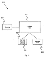
- Fig. 2 illustrates a block diagram of a digital signal processing circuit 200 for implementing an arithmetic shifter and saturation detection circuit according to an embodiment of the present invention.
- Fig. 2 shows a control unit 210, a data unit 220 and an address unit 230.
- the control unit 210 directs the operation of the digital signal processor based on an instruction set (ISA) optimised for the task of rapid signal processing.
- ISA instruction set
- the signal processing is divided between the control unit 210 that directs program flow and one or more execution units that perform operations on data. Almost always, a collection of registers/memory 240 is included to hold operands and intermediate results.
- One of the execution units is the address unit 230.
- the address unit 230 directs the operand fetch for all variables which are defined and used by the executing instructions or program.
- Another execution unit is the data unit 220, which includes at least one arithmetic logic unit 222 that accepts as inputs the data to be operated on and a code from the control unit 210 indicating what operation to perform.
- the arithmetic logic unit 222 provides the result of the computation and may indicate cases such as carry-in or carry-out, overflow, underflow and/or other statuses.
- Fig. 3 is a flow chart 300 of the method for providing a shift process with saturation for digital signal processor operations according to an embodiment of the present invention.
- data and shift amount values are provided to an arithmetic shifter 310.
- the arithmetic shifter provides an output to maximum shifter and to minimum shifter 312.
- An underflow and overflow detection circuit detect underflow and overflow based on the content of the minimum shifter and the maximum shifter 314.
- a saturation decision multiplexor receives input from the underflow and overflow detection circuits 316.
- a final decision multiplexor receives the output from the arithmetic shifter and the saturated value from the output multiplexor 318.
- Whether saturation occurs is determined by the final decision multiplexor using the output of the saturation decision multiplexor, the most significant bit of the arithmetic shifter output, and the most significant bit of data in 320. Saturation is detected if the most significant bit of the arithmetic shifter output and the most significant bit of data in are different or if the saturation decision multiplexor so indicates.
- the final decision multiplexor selects the saturate minimum or the saturate maximum depending on whether the MSB equals one or zero, respectively 330. Else 324, the final decision multiplexor selects the output from the arithmetic shifter 340.
- a digital signal processor as illustrated above with respect to Figs. 1-3 may be used in a wide variety of products such as field programmable gate arrays, personal digital assistants (PDAs), cellular phones, digital scanners, digital cameras, personal computers and storage controllers.
- Fig. 4 shows one example wherein a magnetic disk drive includes a hard drive controller and microprocessor unit.
- the hard drive controller, microprocessor and memory e.g., SRAM, may be shown separately, such components could easily be combined into one component, e.g., the hard drive controller.
- Fig. 4 shows a schematic block diagram showing a hard disk storage system 400 according to one embodiment of the present invention.
- the hard disk storage system 400 is connected to a host computer 432.
- the hard disk storage system 400 responds to the write request by the host computer 432 and records the recording data from the host computer 432 on a magnetic disk 410, which serves as a recording medium.
- the hard disk storage system 400 further responds to the read request from the host computer 432, reads the data recorded on the magnetic disk 410, and sends the data to the host computer 432.
- the hard disk storage system 400 includes the magnetic disk 410, first and second motors 412, 416, a head device 414, a signal processing circuit 420, a servo circuit 430, a microprocessor (MPU) 440, a memory (RAM) 450, a hard drive controller (HDC) 460, and an interface circuit 470.
- the circuits 420-470 are connected to one another by a bus 480.
- the magnetic disk 410 is rotated by the first motor 412 at a constant rotating speed.
- the second motor 416 controls the head device 414 so that it moves in the radial direction with respect to the magnetic disk 410.
- the head device 414 reads the data recorded on the magnetic disk 410 and sends a read signal, RD, to the signal processing circuit 420.
- the signal processing circuit 420 samples the read signal, RD, in synchronism with a clock signal and generates a digital read signal.
- the signal processing circuit 420 carries out a decoding process on the digital read signal and outputs the decoded data signal.
- the servo circuit 430 controls the first motor 412 and rotates the magnetic disk 410 at a constant speed.
- the servo circuit 430 further receives the decoded data signal from the signal processing circuit 420 via the bus 480 and controls the second motor 416 based on the servo data included in the digital read signal so that the head device 414 is on track at the target position.
- the MPU 440 analyzes the write/read processing command sent from the host computer 432 in accordance with the program data stored in the RAM 450 and sends a control signal to the HDC 460 via the bus 480.
- the HDC 460 controls the signal processing circuit 420 and the servo circuit 430 in accordance with the control signal from the MPU 440.
- the HDC 460 further receives a data signal from the signal processing circuit 420 via the bus 480.
- the HDC 460 processes date, e.g., performs an error correcting code (ECC) process on the data signal.
- ECC error correcting code
- the interface circuit 470 converts the data from the HDC 460 to a predetermined communication mode and sends the converted data to the host computer 432.
- the MPU 440 includes an arithmetic logic unit including an arithmetic shifter and saturation detection circuit as illustrated in Fig. 1 for shifting an operand to either maximum or the minimum value depending on the bit of data input when saturation occurs.
- the HDC 460 sends a single shift instruction to the MPU 440.
- the MPU 440 may be configured so that the shift instruction may be run by firmware of the HDC 460.
- the MPU 440 returns a shifted operand or a minimum/maximum saturation value.
- the MPU 440 could include a standalone processor or an embedded processor, e.g., the MPU 440 could be embedded in the HDC 460.
- the MPU 440 could be part of a system on a chip (SOC).
- the MPU 440 could be an ASIC, which would be hardware circuits that perform the function of the processor operating pursuant to memory 450. In such a situation, memory 450 may be used but is not required, as the ASIC is designed to perform any assigned functions. It should also be appreciated that memory 450 could be either volatile or non-volatile memory.
- the MPU 440 controls the operation of the voice coil motor 416 and spindle motor 412 via the servo unit 430.
Landscapes
- Engineering & Computer Science (AREA)
- Theoretical Computer Science (AREA)
- Physics & Mathematics (AREA)
- General Physics & Mathematics (AREA)
- General Engineering & Computer Science (AREA)
- Computational Mathematics (AREA)
- Signal Processing (AREA)
- Computing Systems (AREA)
- Mathematical Analysis (AREA)
- Mathematical Optimization (AREA)
- Pure & Applied Mathematics (AREA)
- Executing Machine-Instructions (AREA)
- Complex Calculations (AREA)
Applications Claiming Priority (1)
| Application Number | Priority Date | Filing Date | Title |
|---|---|---|---|
| US11/068,206 US8209366B2 (en) | 2005-02-28 | 2005-02-28 | Method, apparatus and program storage device that provides a shift process with saturation for digital signal processor operations |
Publications (1)
| Publication Number | Publication Date |
|---|---|
| EP1696314A1 true EP1696314A1 (fr) | 2006-08-30 |
Family
ID=36102994
Family Applications (1)
| Application Number | Title | Priority Date | Filing Date |
|---|---|---|---|
| EP06000180A Withdrawn EP1696314A1 (fr) | 2005-02-28 | 2006-01-05 | Unité de décalage arithmétique, unité de traitement et dispositif de stockage |
Country Status (3)
| Country | Link |
|---|---|
| US (1) | US8209366B2 (fr) |
| EP (1) | EP1696314A1 (fr) |
| CN (1) | CN100495316C (fr) |
Cited By (2)
| Publication number | Priority date | Publication date | Assignee | Title |
|---|---|---|---|---|
| GB2525961A (en) * | 2014-03-20 | 2015-11-11 | Advanced Risc Mach Ltd | Predicting saturation in a shift operation |
| CN112181354A (zh) * | 2020-10-12 | 2021-01-05 | 上海芯旺微电子技术有限公司 | 一种移位饱和同步处理的方法及其应用 |
Families Citing this family (4)
| Publication number | Priority date | Publication date | Assignee | Title |
|---|---|---|---|---|
| US8280941B2 (en) * | 2007-12-19 | 2012-10-02 | HGST Netherlands B.V. | Method and system for performing calculations using fixed point microprocessor hardware |
| US20090164544A1 (en) * | 2007-12-19 | 2009-06-25 | Jeffrey Dobbek | Dynamic range enhancement for arithmetic calculations in real-time control systems using fixed point hardware |
| US9747105B2 (en) * | 2009-12-17 | 2017-08-29 | Intel Corporation | Method and apparatus for performing a shift and exclusive or operation in a single instruction |
| CN112181355B (zh) * | 2020-10-12 | 2021-08-06 | 上海芯旺微电子技术有限公司 | 一种移位饱和处理方法及其应用 |
Citations (4)
| Publication number | Priority date | Publication date | Assignee | Title |
|---|---|---|---|---|
| US5745393A (en) * | 1996-10-17 | 1998-04-28 | Samsung Electronics Company, Ltd. | Left-shifting an integer operand and providing a clamped integer result |
| US5784532A (en) * | 1994-02-16 | 1998-07-21 | Qualcomm Incorporated | Application specific integrated circuit (ASIC) for performing rapid speech compression in a mobile telephone system |
| EP1058185A1 (fr) * | 1999-05-31 | 2000-12-06 | Motorola, Inc. | Un appareil de multiplication et d'accumulation et son procédé |
| US6321248B1 (en) * | 1997-12-23 | 2001-11-20 | Stmicroelectronics S.A. | Process for determining an overflow to the format of the result of an arithmetic operation carried out on two operands |
Family Cites Families (25)
| Publication number | Priority date | Publication date | Assignee | Title |
|---|---|---|---|---|
| US3812470A (en) | 1972-07-31 | 1974-05-21 | Westinghouse Electric Corp | Programmable digital signal processor |
| JPH0628051B2 (ja) * | 1986-04-25 | 1994-04-13 | 株式会社日立製作所 | 記憶制御方式 |
| US5241490A (en) | 1992-01-06 | 1993-08-31 | Intel Corporation | Fully decoded multistage leading zero detector and normalization apparatus |
| US5557183A (en) * | 1993-07-29 | 1996-09-17 | International Business Machines Corporation | Method and apparatus for predicting failure of a disk drive |
| US5448509A (en) * | 1993-12-08 | 1995-09-05 | Hewlett-Packard Company | Efficient hardware handling of positive and negative overflow resulting from arithmetic operations |
| JP3105738B2 (ja) * | 1994-06-10 | 2000-11-06 | 日本電気株式会社 | 情報処理装置 |
| US5959636A (en) * | 1996-02-23 | 1999-09-28 | Intel Corporation | Method and apparatus for performing saturation instructions using saturation limit values |
| US5960200A (en) * | 1996-05-03 | 1999-09-28 | I-Cube | System to transition an enterprise to a distributed infrastructure |
| US5706217A (en) * | 1996-07-30 | 1998-01-06 | Hughes Aircraft | Digital signal processing automatic gain control amplifier |
| JP3701401B2 (ja) * | 1996-08-12 | 2005-09-28 | 株式会社ルネサステクノロジ | 飽和演算命令を有するマイクロプロセッサ |
| US5844827A (en) * | 1996-10-17 | 1998-12-01 | Samsung Electronics Co., Ltd. | Arithmetic shifter that performs multiply/divide by two to the nth power for positive and negative N |
| KR100236533B1 (ko) * | 1997-01-16 | 2000-01-15 | 윤종용 | 배럴 쉬프터와 산술논리 연산기가 연결되어 있는 디지탈 신호 처리기 및 그 오버플로 검출방법 |
| US6078940A (en) * | 1997-01-24 | 2000-06-20 | Texas Instruments Incorporated | Microprocessor with an instruction for multiply and left shift with saturate |
| US6453464B1 (en) * | 1998-09-03 | 2002-09-17 | Legacyj. Corp., Inc. | Method and apparatus for converting COBOL to Java |
| GB2343970A (en) * | 1998-11-20 | 2000-05-24 | Advanced Risc Mach Ltd | Arithmetic operations in a data processing system |
| US6523171B1 (en) * | 1998-12-29 | 2003-02-18 | International Business Machines Corporation | Enhanced source code translator from procedural programming language (PPL) to an object oriented programming language (OOPL) |
| JP2001167040A (ja) * | 1999-12-14 | 2001-06-22 | Hitachi Ltd | 記憶サブシステム及び記憶制御装置 |
| US6757819B1 (en) * | 2000-02-18 | 2004-06-29 | Texas Instruments Incorporated | Microprocessor with instructions for shifting data responsive to a signed count value |
| US7206800B1 (en) * | 2000-08-30 | 2007-04-17 | Micron Technology, Inc. | Overflow detection and clamping with parallel operand processing for fixed-point multipliers |
| JP3833884B2 (ja) * | 2000-09-27 | 2006-10-18 | 株式会社東芝 | ディジタルフィルタ |
| US7073118B2 (en) * | 2001-09-17 | 2006-07-04 | Digeo, Inc. | Apparatus and method for saturating decoder values |
| US6822654B1 (en) * | 2001-12-31 | 2004-11-23 | Apple Computer, Inc. | Memory controller chipset |
| US7103621B2 (en) * | 2002-03-29 | 2006-09-05 | Pts Corporation | Processor efficient transformation and lighting implementation for three dimensional graphics utilizing scaled conversion instructions |
| EP1387259B1 (fr) * | 2002-07-31 | 2017-09-20 | Texas Instruments Incorporated | Controle interprocesseur |
| US20060031272A1 (en) * | 2004-08-05 | 2006-02-09 | International Business Machines Corporation | Alignment shifter supporting multiple precisions |
-
2005
- 2005-02-28 US US11/068,206 patent/US8209366B2/en active Active
-
2006
- 2006-01-05 EP EP06000180A patent/EP1696314A1/fr not_active Withdrawn
- 2006-02-27 CN CNB2006100549550A patent/CN100495316C/zh not_active Expired - Fee Related
Patent Citations (4)
| Publication number | Priority date | Publication date | Assignee | Title |
|---|---|---|---|---|
| US5784532A (en) * | 1994-02-16 | 1998-07-21 | Qualcomm Incorporated | Application specific integrated circuit (ASIC) for performing rapid speech compression in a mobile telephone system |
| US5745393A (en) * | 1996-10-17 | 1998-04-28 | Samsung Electronics Company, Ltd. | Left-shifting an integer operand and providing a clamped integer result |
| US6321248B1 (en) * | 1997-12-23 | 2001-11-20 | Stmicroelectronics S.A. | Process for determining an overflow to the format of the result of an arithmetic operation carried out on two operands |
| EP1058185A1 (fr) * | 1999-05-31 | 2000-12-06 | Motorola, Inc. | Un appareil de multiplication et d'accumulation et son procédé |
Non-Patent Citations (1)
| Title |
|---|
| ONOYE T ET AL: "Low-power implementation of H.324 audiovisual codec dedicated to mobile computing", DESIGN AUTOMATION CONFERENCE 1998. PROCEEDINGS OF THE ASP-DAC '98. ASIA AND SOUTH PACIFIC YOKOHAMA, JAPAN 10-13 FEB. 1998, NEW YORK, NY, USA,IEEE, US, 10 February 1998 (1998-02-10), pages 589 - 594, XP010275953, ISBN: 0-7803-4425-1 * |
Cited By (6)
| Publication number | Priority date | Publication date | Assignee | Title |
|---|---|---|---|---|
| GB2525961A (en) * | 2014-03-20 | 2015-11-11 | Advanced Risc Mach Ltd | Predicting saturation in a shift operation |
| US9208839B2 (en) | 2014-03-20 | 2015-12-08 | Arm Limited | Predicting saturation in a shift operation |
| US9564187B2 (en) | 2014-03-20 | 2017-02-07 | Arm Limited | Predicting saturation in a shift operation |
| GB2525961B (en) * | 2014-03-20 | 2021-05-05 | Advanced Risc Mach Ltd | Predicting saturation in a shift operation |
| CN112181354A (zh) * | 2020-10-12 | 2021-01-05 | 上海芯旺微电子技术有限公司 | 一种移位饱和同步处理的方法及其应用 |
| CN112181354B (zh) * | 2020-10-12 | 2021-08-10 | 上海芯旺微电子技术有限公司 | 一种移位饱和同步处理的方法及其应用 |
Also Published As
| Publication number | Publication date |
|---|---|
| US20060195497A1 (en) | 2006-08-31 |
| US8209366B2 (en) | 2012-06-26 |
| CN1828520A (zh) | 2006-09-06 |
| CN100495316C (zh) | 2009-06-03 |
Similar Documents
| Publication | Publication Date | Title |
|---|---|---|
| US11588497B2 (en) | Floating point to fixed point conversion using exponent offset | |
| US12417073B2 (en) | Floating point to fixed point conversion | |
| JP3549549B2 (ja) | 算術論理ユニット | |
| US6108772A (en) | Method and apparatus for supporting multiple floating point processing models | |
| US5422805A (en) | Method and apparatus for multiplying two numbers using signed arithmetic | |
| EP1058185A1 (fr) | Un appareil de multiplication et d'accumulation et son procédé | |
| JP5102288B2 (ja) | 精度制御反復算術論理演算ユニット | |
| WO1994006075A1 (fr) | Procede et appareil de discrimination de caracteres non numeriques | |
| US9870200B2 (en) | Decimal and binary floating point rounding | |
| EP1696314A1 (fr) | Unité de décalage arithmétique, unité de traitement et dispositif de stockage | |
| US5790444A (en) | Fast alignment unit for multiply-add floating point unit | |
| JPH0786826B2 (ja) | 整数除算回路 | |
| US7716268B2 (en) | Method and apparatus for providing a processor based nested form polynomial engine | |
| US7668892B2 (en) | Data processing apparatus and method for normalizing a data value | |
| JP3012357B2 (ja) | シフト量検出回路 | |
| KR20250020590A (ko) | 레지스터 기반 룩업 테이블을 보간하기 위한 시스템 및 방법 | |
| US6615228B1 (en) | Selection based rounding system and method for floating point operations | |
| US7386580B2 (en) | Data processing apparatus and method for computing an absolute difference between first and second data elements | |
| US8301680B2 (en) | Apparatus and method to compute reciprocal approximations | |
| KR100385233B1 (ko) | 데이터 프로세싱 시스템의 익스포넌트 유닛 | |
| JP2591250B2 (ja) | データ処理装置 | |
| JPH03245225A (ja) | 浮動小数点加減算装置 | |
| JPH0553759A (ja) | 固定小数点演算ユニツト | |
| JPH03245226A (ja) | 浮動小数点乗算装置 | |
| JPWO1994006075A1 (ja) | 非数値判定方法および装置 |
Legal Events
| Date | Code | Title | Description |
|---|---|---|---|
| PUAI | Public reference made under article 153(3) epc to a published international application that has entered the european phase |
Free format text: ORIGINAL CODE: 0009012 |
|
| AK | Designated contracting states |
Kind code of ref document: A1 Designated state(s): AT BE BG CH CY CZ DE DK EE ES FI FR GB GR HU IE IS IT LI LT LU LV MC NL PL PT RO SE SI SK TR |
|
| AX | Request for extension of the european patent |
Extension state: AL BA HR MK YU |
|
| 17P | Request for examination filed |
Effective date: 20070228 |
|
| 17Q | First examination report despatched |
Effective date: 20070402 |
|
| AKX | Designation fees paid |
Designated state(s): DE FR GB |
|
| STAA | Information on the status of an ep patent application or granted ep patent |
Free format text: STATUS: THE APPLICATION HAS BEEN WITHDRAWN |
|
| 18W | Application withdrawn |
Effective date: 20081010 |