EP1699086A1 - Procede de fabrication de dispositif a semi-conducteur et dispositif a semi-conducteur - Google Patents
Procede de fabrication de dispositif a semi-conducteur et dispositif a semi-conducteur Download PDFInfo
- Publication number
- EP1699086A1 EP1699086A1 EP04808082A EP04808082A EP1699086A1 EP 1699086 A1 EP1699086 A1 EP 1699086A1 EP 04808082 A EP04808082 A EP 04808082A EP 04808082 A EP04808082 A EP 04808082A EP 1699086 A1 EP1699086 A1 EP 1699086A1
- Authority
- EP
- European Patent Office
- Prior art keywords
- layer
- layers
- trench
- conductivity
- resurf
- Prior art date
- Legal status (The legal status is an assumption and is not a legal conclusion. Google has not performed a legal analysis and makes no representation as to the accuracy of the status listed.)
- Withdrawn
Links
Images




Classifications
-
- H—ELECTRICITY
- H10—SEMICONDUCTOR DEVICES; ELECTRIC SOLID-STATE DEVICES NOT OTHERWISE PROVIDED FOR
- H10D—INORGANIC ELECTRIC SEMICONDUCTOR DEVICES
- H10D30/00—Field-effect transistors [FET]
- H10D30/60—Insulated-gate field-effect transistors [IGFET]
- H10D30/64—Double-diffused metal-oxide semiconductor [DMOS] FETs
- H10D30/66—Vertical DMOS [VDMOS] FETs
-
- H—ELECTRICITY
- H10—SEMICONDUCTOR DEVICES; ELECTRIC SOLID-STATE DEVICES NOT OTHERWISE PROVIDED FOR
- H10D—INORGANIC ELECTRIC SEMICONDUCTOR DEVICES
- H10D30/00—Field-effect transistors [FET]
- H10D30/01—Manufacture or treatment
- H10D30/021—Manufacture or treatment of FETs having insulated gates [IGFET]
- H10D30/028—Manufacture or treatment of FETs having insulated gates [IGFET] of double-diffused metal oxide semiconductor [DMOS] FETs
- H10D30/0291—Manufacture or treatment of FETs having insulated gates [IGFET] of double-diffused metal oxide semiconductor [DMOS] FETs of vertical DMOS [VDMOS] FETs
-
- H—ELECTRICITY
- H10—SEMICONDUCTOR DEVICES; ELECTRIC SOLID-STATE DEVICES NOT OTHERWISE PROVIDED FOR
- H10D—INORGANIC ELECTRIC SEMICONDUCTOR DEVICES
- H10D62/00—Semiconductor bodies, or regions thereof, of devices having potential barriers
- H10D62/10—Shapes, relative sizes or dispositions of the regions of the semiconductor bodies; Shapes of the semiconductor bodies
- H10D62/102—Constructional design considerations for preventing surface leakage or controlling electric field concentration
- H10D62/103—Constructional design considerations for preventing surface leakage or controlling electric field concentration for increasing or controlling the breakdown voltage of reverse-biased devices
- H10D62/105—Constructional design considerations for preventing surface leakage or controlling electric field concentration for increasing or controlling the breakdown voltage of reverse-biased devices by having particular doping profiles, shapes or arrangements of PN junctions; by having supplementary regions, e.g. junction termination extension [JTE]
- H10D62/109—Reduced surface field [RESURF] PN junction structures
- H10D62/111—Multiple RESURF structures, e.g. double RESURF or 3D-RESURF structures
-
- H—ELECTRICITY
- H10—SEMICONDUCTOR DEVICES; ELECTRIC SOLID-STATE DEVICES NOT OTHERWISE PROVIDED FOR
- H10D—INORGANIC ELECTRIC SEMICONDUCTOR DEVICES
- H10D62/00—Semiconductor bodies, or regions thereof, of devices having potential barriers
- H10D62/10—Shapes, relative sizes or dispositions of the regions of the semiconductor bodies; Shapes of the semiconductor bodies
- H10D62/113—Isolations within a component, i.e. internal isolations
- H10D62/115—Dielectric isolations, e.g. air gaps
- H10D62/116—Dielectric isolations, e.g. air gaps adjoining the input or output regions of field-effect devices, e.g. adjoining source or drain regions
-
- H—ELECTRICITY
- H10—SEMICONDUCTOR DEVICES; ELECTRIC SOLID-STATE DEVICES NOT OTHERWISE PROVIDED FOR
- H10D—INORGANIC ELECTRIC SEMICONDUCTOR DEVICES
- H10D64/00—Electrodes of devices having potential barriers
- H10D64/111—Field plates
- H10D64/117—Recessed field plates, e.g. trench field plates or buried field plates
-
- H—ELECTRICITY
- H10—SEMICONDUCTOR DEVICES; ELECTRIC SOLID-STATE DEVICES NOT OTHERWISE PROVIDED FOR
- H10D—INORGANIC ELECTRIC SEMICONDUCTOR DEVICES
- H10D64/00—Electrodes of devices having potential barriers
- H10D64/20—Electrodes characterised by their shapes, relative sizes or dispositions
- H10D64/23—Electrodes carrying the current to be rectified, amplified, oscillated or switched, e.g. sources, drains, anodes or cathodes
- H10D64/251—Source or drain electrodes for field-effect devices
- H10D64/252—Source or drain electrodes for field-effect devices for vertical or pseudo-vertical devices
-
- H—ELECTRICITY
- H10—SEMICONDUCTOR DEVICES; ELECTRIC SOLID-STATE DEVICES NOT OTHERWISE PROVIDED FOR
- H10P—GENERIC PROCESSES OR APPARATUS FOR THE MANUFACTURE OR TREATMENT OF DEVICES COVERED BY CLASS H10
- H10P30/00—Ion implantation into wafers, substrates or parts of devices
- H10P30/20—Ion implantation into wafers, substrates or parts of devices into semiconductor materials, e.g. for doping
- H10P30/222—Ion implantation into wafers, substrates or parts of devices into semiconductor materials, e.g. for doping characterised by the angle between the ion beam and the crystal planes or the main crystal surface
Definitions
- the present invention relates to a semiconductor device having a so-called super junction structure and to a production method therefor.
- MOS field effect transistor metal oxide semiconductor field effect transistor, MOS FET
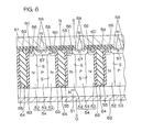
- Fig. 6 is a schematic sectional view of a prior art semiconductor device including MOS FETs (see Japanese Unexamined Patent Publication No. 2003-46082).
- a semiconductor layer 54 including N-type drift layers (N-type pillar layers) 52 and P-type RESURF (reduced surface field) layers (P-type pillar layers) 53 is provided on an N ++ -type semiconductor substrate 51.
- the drift layers 52 and the RESURF layers 53 are recurrently arranged in alternate relation in a direction parallel to the semiconductor substrate 51 to provide a so-called super junction structure.
- a plurality of trenches 55 are provided in the semiconductor layer 54 as extending thicknesswise of the semiconductor layer 54 and having a depth such as to reach an interface between the semiconductor substrate 51 and the semiconductor layer 54.
- the trenches 55 each have interior side walls generally perpendicular to the semiconductor substrate 51, and are generally equidistantly arranged parallel to each other.
- the interior walls of the trenches 55 are each covered with an oxide film 63, and the insides of the trenches 55 are each filled with a buried layer 64 such as of polysilicon or a dielectric material.
- the drift layers 52 are each disposed alongside the trench 55.
- the RESURF layers 53 are each disposed between a pair of drift layers 52 disposed alongside each adjacent pair of trenches 55.
- the RESURF layer 53 contacts the pair of drift layers 52 and the semiconductor substrate 51.
- N-type regions 56 are each provided on the drift layer 52.
- P-type base layers 57 are each provided on the RESURF layer 53 in contact with the adjacent N-type regions 56.
- N-type source regions 58 are provided in a surface portion of each of the base layers 57.
- Gate electrodes 60 are each disposed in opposed relation to a region including portions of the base layers 57 between the N-type regions 56 and the source regions 58 with the intervention of an insulative film 59.
- a source electrode 61 is provided in contact with the source regions 58 and the base layers 57.
- a drain electrode 62 is provided on a back surface of the semiconductor substrate 51 (opposite from a surface of the semiconductor substrate formed with the gate electrodes 60 and the source electrode 61).
- the semiconductor device is used in such a state that, with one of the source electrode 61 and the drain electrode 62 connected to an external load, a predetermined voltage from a power source is applied between the external load and the other of the source electrode 61 and the drain electrode 62.
- the applied voltage provides a reverse bias to PN junctions defined between the RESURF layers 53 and the drift layers 52.
- the gate electrodes 60 are kept at a proper potential (the MOS FETs are turned on), whereby electric currents flow between the source electrode 61 and the drain electrode 62.
- channels are formed in the portions of the base layers 57 between the N-type regions 56 and the source regions 58 in the vicinity of interfaces between the insulative films 59 and the base layers 57.
- the electric currents flow from the drain electrode 62 to the source electrode 61 through the semiconductor substrate 51, the drift layers 52, the N-type regions 56, the portions of the base layers 57 adjacent to the interfaces between the insulative films 59 and the base layers 57 (the channels) and the source regions 58.
- the RESURF layers 53 also contact the semiconductor substrate 51 of the N ++ -type conductivity. Therefore, when the reverse bias voltage is applied to the PN junctions defined between the drift layers 52 and the RESURF layers 53, depletion layers also spread into the RESURF layers 53 and the semiconductor substrate 51 from interfaces between the RESURF layers 53 and the semiconductor substrate 51.
- the depletion layers spread in regions adjacent to the interfaces S between the drift layers 52 and the RESURF layers 53 and in regions adjacent to the interfaces between the semiconductor substrate 51 and the RESURF layers 53 in different manners, because the semiconductor substrate 51 and the drift layers 52 have different impurity concentrations. Therefore, when the semiconductor device is off, strong electric fields locally occur in the depletion layers, so that the electric currents flow in strong electric field regions. Therefore, the breakdown voltage of the semiconductor device is not satisfactory in practice.
- a semiconductor device production method is a production method for a semiconductor device which includes a super junction structural portion provided on a semiconductor substrate of a first conductivity and including drift layers of the first conductivity and RESURF layers of a second conductivity different from the first conductivity, the drift layers and the RESURF layers being laterally arranged in alternate relation in a direction parallel to the semiconductor substrate.
- the production method comprises the steps of: forming a semiconductor layer of the first conductivity on the semiconductor substrate; forming a trench in the semiconductor layer, the trench penetrating through the semiconductor layer to reach the semiconductor substrate; filling a filling material in a predetermined bottom portion of the trench, so that a filling material portion is provided in the bottom portion of the trench up to a predetermined upper surface position which is shallower than an interface between the semiconductor substrate and the semiconductor layer and a void is provided in an upper portion of the trench above the predetermined upper surface position; and, after the filling step, introducing an impurity of the second conductivity into a portion of the semiconductor layer exposed to an interior side wall of the trench, whereby the RESURF layers of the second conductivity are each formed alongside the interior side wall of the trench and the drift layers are each defined by a portion of the semiconductor layer remaining intact.
- the RESURF layers are each provided alongside the interior side wall of the trench penetrating through the semiconductor layer to reach the semiconductor substrate, and the drift layers are each defined by the portion of the semiconductor layer remaining intact after the formation of the RESURF layer.
- the semiconductor device is produced as having a so-called super junction structure in which the drift layers and the RESURF layers are arranged recurrently (alternately) in a direction parallel to the semiconductor substrate.
- the RESURF layers may be provided alongside only one of widthwise opposite interior side walls of the trench or alongside the widthwise opposite interior side walls of the trench.
- the filling material portion is present in the bottom portion of the trench, and the upper surface of the filling material portion is located at the position shallower than the interface between the semiconductor substrate and the semiconductor layer as measured from the surface of the semiconductor layer. Therefore, the filling material portion prevents the impurity of the second conductivity (an impurity for control of impartation with the second conductivity) from being introduced into a portion of the semiconductor layer adjacent to the semiconductor substrate.
- the RESURF layers are isolated from the semiconductor substrate by the drift layers (the portions of the semiconductor layer remaining intact).
- depletion layers spread into the drift layers and the RESURF layers from interfaces between the drift layers and the RESURF layers (hereinafter referred to simply as "interfaces") when a reverse bias is applied to PN junctions defined between the drift layers and the RESURF layers.
- interfaces interfaces between the drift layers and the RESURF layers
- the semiconductor device has a predetermined breakdown voltage (e.g., several hundreds volts).
- Semiconductor portions having a generally even impurity concentration are present between the RESURF layer and the semiconductor substrate and between the RESURF layer and the trench or between two adjacent RESURF layers in each of the drift layers. Therefore, the depletion layers uniformly spread from the interfaces in the drift layers. That is, the depletion layers equally spread toward the trenches opposed to the interfaces with the intervention of the drift layers (parallel to the semiconductor substrate), and toward the semiconductor substrate opposed to the interfaces with the intervention of the drift layers (perpendicularly to the semiconductor substrate) in the drift layers from the interfaces.
- the semiconductor device has an increased breakdown voltage (e.g., 200V to 1000V) as compared with the prior art semiconductor device.
- the RESURF layer formation step may include the steps of implanting the impurity of the second conductivity into a surface portion of the semiconductor layer exposed to the interior side wall of the trench, and performing a thermal diffusion process to heat the resulting semiconductor substrate after the implantation step for diffusing the implanted impurity into the semiconductor layer.
- the filling step may include the steps of supplying the filling material into the trench up to a position which is shallower than the predetermined upper surface position and, after the filling material supplying step, etching back the supplied filling material to the predetermined upper surface position.
- the upper surface of the filling material portion can be located at the position shallower than the interface between the semiconductor substrate and the semiconductor layer, so that the position of the upper surface of the filling material portion can be arbitrarily adjusted.
- the width of a portion of the drift layer present between the RESURF layer and the semiconductor substrate can be easily controlled.
- the filling material supplying step may include the step of almost completely filling the trench with the fillingmaterial. That is, the fillingmaterial supplying step may include the step of supplying the filling material so that an upper surface of the filling material is located outside the trench.
- the filling step may include the step of filling silicon oxide as the filling material in the trench.
- the step of filling silicon oxide in the trench may include the steps of filling polysilicon in the trench, and oxidizing the polysilicon to provide silicon oxide as the filling material.
- the step of filling silicon oxide in the trench may include the steps of filling TEOS (tetraethylorthosilicate) in the trench, and thermally decomposing TEOS to provide silicon oxide as the filling material.
- TEOS tetraethylorthosilicate
- the filling step may include the step of filling polysilicon as the filling material in the trench and, in this case, the semiconductor device production method may further comprise the step of forming an oxide film by oxidizing an interior wall of the trench before the filling step.
- the oxide film electrically isolates the filling material (polysilicon) portion from the semiconductor substrate and the super junction structural portion.
- the oxide film formation step may include the step of thermally oxidizing the interior wall of the trench.
- the semiconductor device production method may further comprise the step of filling the void in the upper portion of the trench with an upper filling material after the RESURF layer formation step.
- the semiconductor device can be provided in which the trench is almost completely filled with the filling material and the upper filling material. This prevents the semiconductor substrate from being warped.
- the filling material to be filled in the trench before the RESURF layer formation step and the upper filling material may be of the same type or of different types.
- the inventive semiconductor device production method may further comprise the steps of: introducing an impurity of the second conductivity into a surface portion of the semiconductor layer to form a base region of the second conductivity in contact with the RESURF layer and the drift layer; introducing an impurity of the first conductivity into a portion of the base region to form a source region of the first conductivity which is isolated from the drift layer and the RESURF layer by the other portion of the base region; forming a gate insulation film opposed to a portion of the base region between the source region and the drift layer; and forming a gate electrode opposed to the portion of the base region between the source region and the drift layer with the intervention of the gate insulation film.
- channels are formed in portions of base regions between source regions and the drift layers in the vicinity of gate insulation films by applying a voltage of a proper level between the source regions and the semiconductor substrate (drain region) and keeping gate electrodes at a predetermined potential (turning on the semiconductor device).
- the semiconductor device Even if a higher reverse bias voltage is applied to the PN junctions defined between the drift layers and the RESURF layers when the semiconductor device is off, the semiconductor device has a higher breakdown voltage.
- a semiconductor device comprises a semiconductor substrate of a first conductivity, a super junction structural portion provided on the semiconductor substrate and including drift layers of the first conductivity and RESURF layers of a second conductivity different from the first conductivity, the drift layers and the RESURF layers being laterally arranged in alternate relation in a direction parallel to the semiconductor substrate, and filling material portions each provided in a predetermined bottom portion of a trench penetrating through the super junction structural portion to reach the semiconductor substrate.
- the RESURF layers are each provided alongside an interior side wall of the trench.
- the drift layers each have an isolation region present between the RESURF layer and the semiconductor substrate to prevent the RESURF layer from contacting the semiconductor substrate.
- the filling material portion in the trench has an upper surface located at substantially the same depth as an interface between the isolation region and the RESURF layer as measured from a surface of the super junction structural portion.
- the filling material portion may be composed of an insulative material such as silicon oxide or an electrically conductive material (a semiconductor material) such as silicon (e.g., polysilicon) covered with an insulative material.
- an insulative material such as silicon oxide or an electrically conductive material (a semiconductor material) such as silicon (e.g., polysilicon) covered with an insulative material.
- An upper portion of the trench above the filling material portion may be a void left unfilled, but is preferably filled with a filling material (upper filling material) separately from the formation of the filling material portion.
- the inventive semiconductor device may further comprise base regions of the second conductivity each provided in contact with the drift layer and the RESURF layer, source regions of the first conductivity each provided in contact with the base region and isolated from the drift layer and the RESURF layer by the base region, and gate electrodes each provided in opposed relation to a portion of the base region between the source region and the drift layer with the intervention of a gate insulation film.
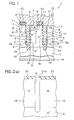
- Fig. 1 is a schematic sectional view illustrating the construction of a semiconductor device according to a first embodiment of the present invention.
- a super junction structural portion 13 having a so-called super junction structure is provided on a silicon substrate 2 of an N + -type conductivity serving as a drain region.
- the super junction structural portion 13 includes drift layers 3 of an N - -type conductivity and RESURF layers 9 of a P - -type conductivity buried in the respective drift layers 3.
- the drift layers 3 and the RESURF layers 9 are alternately (recurrently) arranged in a direction parallel to the silicon substrate 2.
- a plurality of trenches 4 are provided generally parallel to each other as penetrating through the super junction structural portion 13 and having a depth such as to reach the silicon substrate 2.
- the trenches 4 each have interior side walls generally perpendicular to the silicon substrate 2, and extend perpendicularly to a paper face of Fig. 1. That is, the trenches 4 each have a length perpendicular to the paper face of Fig. 1, and a width parallel to the paper face of Fig. 1 and parallel to the silicon substrate 2.
- the semiconductor device 1 has a greater number of trenches 4, which are equidistantly arranged.
- silicon oxide portions 15 are provided in bottoms of the trenches 4, and polysilicon portions 16 are provided on the silicon oxide portions 15.
- Silicon oxide films 5 are respectively present between the trenches 4 and the polysilicon portions 16.
- the trenches 4 are each almost completely filled with the silicon oxide portion 15 and the polysilicon portion 16. Thus, the silicon substrate 2 is less liable to be warped.
- the RESURF layers 9 are each disposed alongside an interior side wall of the trench 4 on one of widthwise opposite sides of the trench. That is, the RESURF layer 9 is disposed between two adjacent trenches 4 in the vicinity of one of these trenches 4 in contact with the silicon oxide film 5.
- the drift layers 3 are each disposed parallel to the RESURF layer 9 between two adjacent RESURF layers 9 (between the RESURF layer 9 and the trench 4) alongside an interior side wall of the trench 4 on the other widthwise side of the trench. Further, the drift layer 3 is partly present below the RESURF layer 9 (between the silicon substrate 2 and the RESURF layer 9). That is, the RESURF layer 9 is isolated from the silicon substrate 2 by the drift layer 3, so that the RESURF layer 9 does not contact the silicon substrate 2.
- a portion 3 H of the drift layer 3 defined between the RESURF layer 9 and the trench 4 is continuous to a portion 3 v (hereinafter referred to as "isolation region") of the drift layer 3 defined between the RESURF layer 9 and the silicon substrate 2 (drain region).
- the drift layer 3 has a generally uniform impurity concentration, so that the portion 3 H between the RESURF layer 9 and the trench 4 and the isolation region 3 v have substantially the same impurity concentration.
- the position D 1 of an interface between the isolation region 3 v and the RESURF layer 9 (the position of an interface between a portion 9a of the RESURF layer 9 opposed to the silicon substrate 2 and the drift layer 3) and the position D 2 of an upper surface of the silicon oxide portion 15 (an interface between the silicon oxide portion 15 and the polysilicon portion 16) are at substantially the same depth as measured from a surface of the super junction structural portion 13. Therefore, the position D 2 of the upper surface of the silicon oxide portion 15 is shallower than an interface between the silicon substrate 2 and the drift layer 3 as measured from a surface of the drift layer 3.
- a source region 7 of an N + -type conductivity is provided in a surface portion of the super junction structural portion 13 (on the RESURF layer 9) adjacent to the trench 4.
- a base region 8 of a P - -type conductivity is provided between the source region 7 and the drift layer 3, between the source region 7 and the RESURF layer 9 and between the source region 7 and the silicon oxide film 5.
- a gate electrode 10 is disposed in the vicinity of the surface of the drift layer 3 in opposed relation to a portion of the base region 8 between the drift layer 3 and the source region 7, and portions of the drift layer 3 and the source region 7 adjacent to this portion.
- the gate electrode 10 is composed of polysilicon imparted with electrical conductivity by introduction of an impurity.
- the gate electrode 10 is covered with a silicon oxide film 11. Therefore, the gate electrode 10 is isolated from the base region 8 by the silicon oxide film 11.
- a source electrode 12 of aluminum is provided on a surface of the silicon substrate 2 formed with the drift layers 3 and the RESURF layers 9.
- the source electrode 12 is electrically connected to the source region 7 and the base region 8.
- a drain electrode 14 is provided on a back surface of the silicon substrate 2 (opposite from the source electrode 12).
- the semiconductor device 1 is used in such a state that, with one of the source electrode 12 and the drain electrode 14 connected to an external load, a predetermine voltage (e.g., several hundreds volts) from a power source is applied between the external load and the other of the source electrode 12 and the drain electrode 14.
- a predetermine voltage e.g., several hundreds volts
- the applied voltage provides a reverse bias to PN junctions defined between the RESURF layers 9 and the drift layers 3.
- the gate electrodes 10 are kept at a predetermined potential (the semiconductor device 1 is turned on), whereby electric currents flow between the source electrode 12 and the drain electrode 14. At this time, channels are formed in the portions of the base regions 8 between the drift layers 3 and the source regions 7 adjacent to the interfaces between the silicon oxide films 11 and the base regions 8.
- a reverse bias (e.g., 2V) resulting from voltage division between the external load and the ON-resistances of MOS FETs is applied to the PN junctions defined between the RESURF layers 9 and the drift layers 3.
- depletion layers occurring due to the reverse bias spread to a negligible extent, so that carrier (electron) paths are present in the drift layers 3.
- the electric currents flow between the source electrode 12 and the drain electrode 14 through non-depleted portions of the drift layers 3.
- the semiconductor device 1 when the semiconductor device 1 is off, i.e., when the gate electrodes 10 are not kept at the predetermined potential, the channels are not formed, so that no electric current flows in the MOS FETs. Therefore, the whole source voltage is applied as a reverse bias to the PN junctions defined between the drift layers 3 and the RESURF layers 9. Hence, the depletion layers spread into the drift layers 3 and the RESURF layers 9 from interfaces S between the drift layers 3 and the RESURF layers 9 in the vicinity of the interfaces S. In the drift layers 3, the depletion layers immediately spread from the interfaces S toward the trenches 4 and the silicon substrate 2 which are opposed to the interfaces S with the intervention of the drift layers 3.
- the depletion layers uniformly spread from the interfaces S into the drift layers 3 having a generally uniform impurity concentration, locally strong electric fields do not occur. Therefore, the electric currents do not easily flow through the interfaces S, so that the semiconductor device 1 has a higher breakdown voltage.
- the semiconductor device 1 has a higher breakdown voltage. Further, the ON-resistances can be reduced by increasing the impurity concentrations of the drift layers 3 defining parts of the electric conduction paths in the ON state.
- the semiconductor device 1 typically has a breakdown voltage of about 200V to about 1000V. Where the semiconductor device has a breakdown voltage of 600V, for example, the semiconductor device has an ON-resistance which is about one fifth of that of the prior art semiconductor device.
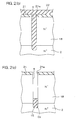
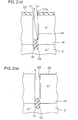
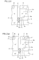
- Figs. 2 (a) to 2 (h) are schematic sectional views for explaining a production method for the semiconductor device 1 of Fig. 1. In Figs. 2 (a) to 2 (h) , only a portion of the semiconductor device associated with one trench 4 is shown.
- an epitaxial layer 18 of the N - -type conductivity is formed on a silicon substrate 2 of the N + -type conductivity, and a hard mask 21 having openings 21a formed in positions corresponding to the trenches 4 is formed on the epitaxial layer 18.
- the hard mask 21 is composed of, for example, silicon nitride.
- the epitaxial layer 18 is dry-etched through the openings 21a of the hard mask 21 (for example, by reactive ion etching), whereby trenches 4 each having a depth such as to reach the silicon substrate 2 are formed in the epitaxial layer 18 as extending thicknesswise of the epitaxial layer.
- the trenches 4 each have a width of, for example, about 2 ⁇ m, and a depth of, for example, about 40 ⁇ m. This state is shown in Fig. 2(a).
- a silicon oxide film 22 is formed over the resulting silicon substrate 2 as filling the insides of the trenches 4 (see Fig. 2(b)).
- the silicon oxide film 22 is also formed on the hard mask 21.
- the formation of the silicon oxide film 22 may be achieved, for example, by forming a polysilicon film to fill the insides of the trenches 4 and then thermally oxidizing the entire polysilicon film, or by forming a TEOS (tetraethylorthosilicate) film by a reduced pressure CVD (chemical vapor deposition) method and then thermally decomposing the TEOS film.
- TEOS tetraethylorthosilicate
- the silicon oxide film 22 except portions thereof present in the bottoms of the trenches 4 is etched back, whereby voids are provided in upper portions of the respective trenches 4.
- the remaining portions of the silicon oxide film 22 serve as the silicon oxide portions 15.
- proper etching-back conditions are selected so that upper surfaces of the silicon oxide portions 15 are located at a position D 2 (predetermined upper surface position) which is shallower than an interface between the silicon substrate 2 and the epitaxial layer 18 as measured from the surface of the epitaxial layer 18. This state is shown in Fig. 2(c).
- P-type impurity ions are implanted into portions of the epitaxial layer 18 exposed to interior surfaces of the trenches 4 through the openings 21a of the hard mask 21.
- the ions are implanted at a predetermined inclination angle with respect to interior side walls of the trenches 4 perpendicular to the widths of the trenches 4 as indicated by arrows A in Fig. 2(d).
- the angle of an ion implantation direction with respect to the interior side walls of the trenches 4 is, for example, 1.5 degrees to 2 degrees.
- a first implanted region 23 implanted with the P-type impurity is formed in substantially the entire interior side wall of each of the trenches 4 on one of widthwise opposite sides of the trench 4 (corresponding to a side of the trench 4 of the semiconductor device 1 where the RESURF layer 9 is provided in proximity to the trench). This state is shown in Fig. 2(d).
- the hard mask 21 is removed, and a resist film (not shown) having openings formed in positions corresponding to the base regions 8 is formed on the epitaxial layer 18. Then, a P-type impurity is implanted into surface portions of the epitaxial layer 18 through the openings of the resist film, whereby second implanted regions 24 are formed. Thereafter, the resist film is removed. This state is shown in Fig. 2(e).
- the resulting silicon substrate 2 is heated to a predetermined temperature, whereby the P-type impurities are diffused into the epitaxial layer 18 from the first and second implanted regions 23, 24.
- the RESURF layers 9 and the base regions 8 are formed.
- the remaining portions of the epitaxial layer 18 serve as the drift layers 3. This state is shown in Fig. 2 (f).
- a resist film (not shown) having openings formed in positions corresponding to the source regions 7 is formed on a surface of the resulting silicon substrate 2 formed with the epitaxial layer 18. Then, an N-type impurity is implanted into surface portions of the base regions 8 through the openings of the resist film, whereby third implanted regions are formed. Thereafter, the resist film is removed, and the resulting silicon substrate 2 is heated to a predetermined temperature, whereby the N-type impurity is diffused into the base regions 8 from the third implanted regions. Thus, the source regions 7 are formed. This state is shown in Fig. 2(g).
- the resulting silicon substrate 2 is heated to a predetermined temperature, whereby an exposed surface portion of the silicon substrate including interior surfaces of the trenches 4 and surfaces of the drift layers 3, the base regions 8 and the source regions 7 is thermally oxidized to form an oxide film 17. Further, a film 19 of polysilicon (polysilicon film) is formed on the oxide film 17. The trenches 4 are almost completely filled with the polysilicon film 19. Thereafter, the polysilicon film 19 is imparted with an electrical conductivity by implantation of an impurity. This state is shown in Fig. 2(h).
- a portion of the polysilicon film 19 other than those corresponding to the insides of the trenches 4 and the gate electrodes 10 is removed.
- the portions of the polysilicon film 19 remaining in the trenches 4 serve as the polysilicon portions 16.
- exposed surface portions of the polysilicon film 19 are thermally oxidized to form oxide films.
- the oxide films on the trenches 4 and the oxide films other than those on peripheral surfaces of the gate electrodes 10 outside the trenches 4 are removed.
- the portions of the polysilicon film remaining outside the trenches 4 serve as the gate electrodes 10.
- the portions of the oxide film 17 remaining in the trenches 4 serve as the silicon oxide films 5, and the oxide films remaining outside the trenches 4 serve as the silicon oxide films 11 covering the peripheral surfaces of the gate electrodes 10.
- the source electrode 12 and the drain electrode 14 are respectively formed on a surface of the resulting silicon substrate 2 formed with the source regions 7 and on a surface of the substrate opposite from the source regions.
- the semiconductor device 1 shown in Fig. 1 is provided.
- the silicon oxide portions 15 are present in the bottoms of the respective trenches 4 up to the position D 2 shallower than the interface between the silicon substrate 2 and the epitaxial layer 18 when the first implanted regions 23 are formed (see Fig. 2(d)). Therefore, the silicon oxide portions 15 prevent the P-type impurity from being introduced into portions of the epitaxial layer 18 adj acent to the silicon substrate 2. Thus, the RESURF layers 9 are isolated from the silicon substrate 2 by the drift layers 3 (isolation regions 3 v ).
- the upper surface position D 2 of the silicon oxide portions 15 can be controlled by controlling the thickness of portions of the silicon oxide film 22 to be etched back (see Fig. 2(c)).
- the RESURF layers 9 can be formed in controlled ranges, so that the thickness of the portions (isolation regions 3 v ) of the drift layers 3 between the silicon substrate 2 and the RESURF layers 9 is controlled to allow the depletion layers to evenly spread from the interfaces S in the semiconductor device 1.
- Fig. 3 is a schematic sectional view of a semiconductor device according to a second embodiment of the present invention.
- parts corresponding to those shown in Fig. 1 will be denoted by the same reference characters as in Fig. 1, and no explanation will be given to these parts.
- a polysilicon portion 32 and an oxide film 33 surrounding the polysilicon portion 32 are provided in the bottom of each of the trenches 4 instead of the silicon oxide portion 15 of the semiconductor device 1 of Fig. 1.
- the inside of the trench 4 is almost completely filled with the polysilicon portions 32, 16 and the oxide film 33.
- the silicon substrate 2 is less liable to be warped.
- the RESURF layers 9 do not contact the silicon substrate 2 (drain region).
- the semiconductor device 31 When the semiconductor device 31 is off, the depletion layers uniformly spread in the drift layers 3 from the interfaces S toward the trenches 4 and the silicon substrate 2 which are opposed to the interfaces S with the intervention of the drift layers 3. Therefore, locally strong electric fields do not occur. Since the electric currents do not easily flow through the interfaces S, the semiconductor device 31 has a higher breakdown voltage.
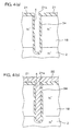
- Figs. 4 (a) to 4 (d) are schematic sectional views for explaining a production method for the semiconductor device 31.
- parts corresponding to those shown in Figs. 2(a) to 2(h) will be denoted by the same reference characters as in Figs. 2(a) to 2(h), and no explanation will be given to these parts.
- the silicon substrate 2 is heated, whereby exposed surfaces of the silicon substrate 2 and the epitaxial layer 18, i.e. , the interior surfaces of the trenches 4, are thermally oxidized to form sacrificial oxide films 34 (see Fig. 4(a)).
- a polysilicon film 35 is formed to almost completely fill the insides of the trenches 4.
- the polysilicon film 35 is also formed outside the trenches 4, i.e., on the hard mask 21 (see Fig. 4(b)).
- the polysilicon film 35 except portions thereof present in the bottoms of the trenches 4 is etched back, whereby voids are formed in the upper portions of the trenches 4.
- the remaining portions of the polysilicon film 35 serve as the polysilicon portions 32.
- the etching-back conditions are determined so that upper surfaces (etched-back surfaces) of the polysilicon portions 32 are each located at a position (predetermined upper surface position) D 2 which is shallower than the interface between the silicon substrate 2 and the epitaxial layer 18 as measured from the surface of the epitaxial layer 18. This state is shown in Fig. 4(c).
- portions of the sacrificial oxide films 34 are etched away. Portions of the sacrificial oxide films 34 present between the polysilicon portions 32 and the silicon substrate 2 and between the polysilicon portions 32 and the epitaxial layer 18 remain.
- the step for the formation of the first implanted regions 23 (see Fig. 4(d)) and the steps subsequent to this step are performed in the same manner as in the production method for the semiconductor device 1.
- the semiconductor device 31 shown in Fig. 3 is provided.
- the upper surfaces (etched-back surfaces) of the polysilicon portions 32 are also oxidized when the oxide film 17 is formed (see Fig. 2(h)).
- the resulting oxide films and the remaining portions of the sacrificial oxide films 34 provide the oxide films 33 which respectively surround the polysilicon portions 32.
- Fig. 5 is a schematic sectional view illustrating the construction of a semiconductor device according to a third embodiment of the present invention.
- parts corresponding to those shown in Fig. 1 will be denoted by the same reference characters as in Fig. 1, and no explanation will be given to these parts.
- This semiconductor device 41 has substantially the same construction as the semiconductor device 1 shown in Fig. 1, except that the RESURF layers 9 are provided on widthwise opposite sides of each of the trenches 4.
- the drift layers 3 are each partly present between the RESURF layers 9 and the silicon substrate 2 serving as the drain region, so that the RESURF layers 9 do not contact the silicon substrate 2.
- the depletion layers uniformly spread from the interfaces S toward the adjacent RESURF layers 9 and toward the silicon substrate 2 in the drift layers 3 each having a generally even impurity concentration, so that locally strong electric fields do not occur.
- the electric currents do not easily flow through the interfaces S. Therefore, the semiconductor device 41 has a higher breakdown voltage.
- the semiconductor device 41 is produced by forming the silicon oxide portions 15 so that the upper surfaces of the silicon oxide portions 15 are each located at the position (predetermined upper surface position) D 2 which is shallower than the interface between the silicon substrate 2 and the epitaxial layer 18 as measured from the surface of the epitaxial layer 18, and then implanting the P-type impurity into widthwise opposite interior side walls of the trenches 4 in the production method for the semiconductor device 1.
- the ions are implanted in two directions which are inclined at a very small inclination angle with respect to the interior side walls of the trenches 4 and extend widthwise of the trenches 4 (perpendicularly to the lengths of the trenches) as seen perpendicularly to the silicon substrate 2.
- the P-type impurity is not introduced into portions of the epitaxial layer 18 adj acent to the silicon substrate 2, so that the RESURF layers 9 are isolated from the silicon substrate 2 by the portions (drift layers 3) of the epitaxial layer 18 remaining intact.
- the sacrificial oxide films 34 may be entirely removed after the formation of the sacrificial film 34 (see Fig. 4(a)), and then oxide films equivalent to the sacrificial films 34 may be formed, followed by the steps subsequent to the step for the formation of the polysilicon film 35.
Landscapes
- Insulated Gate Type Field-Effect Transistor (AREA)
- Electrodes Of Semiconductors (AREA)
- Element Separation (AREA)
Applications Claiming Priority (2)
| Application Number | Priority Date | Filing Date | Title |
|---|---|---|---|
| JP2003435266A JP4699692B2 (ja) | 2003-12-26 | 2003-12-26 | 半導体装置の製造方法および半導体装置 |
| PCT/JP2004/019732 WO2005064684A1 (fr) | 2003-12-26 | 2004-12-24 | Procede de fabrication de dispositif a semi-conducteur et dispositif a semi-conducteur |
Publications (2)
| Publication Number | Publication Date |
|---|---|
| EP1699086A1 true EP1699086A1 (fr) | 2006-09-06 |
| EP1699086A4 EP1699086A4 (fr) | 2008-07-09 |
Family
ID=34736599
Family Applications (1)
| Application Number | Title | Priority Date | Filing Date |
|---|---|---|---|
| EP04808082A Withdrawn EP1699086A4 (fr) | 2003-12-26 | 2004-12-24 | Procede de fabrication de dispositif a semi-conducteur et dispositif a semi-conducteur |
Country Status (6)
| Country | Link |
|---|---|
| US (1) | US7642139B2 (fr) |
| EP (1) | EP1699086A4 (fr) |
| JP (1) | JP4699692B2 (fr) |
| KR (1) | KR20070026308A (fr) |
| CN (1) | CN1823424A (fr) |
| WO (1) | WO2005064684A1 (fr) |
Families Citing this family (23)
| Publication number | Priority date | Publication date | Assignee | Title |
|---|---|---|---|---|
| US7416948B2 (en) * | 2003-12-30 | 2008-08-26 | Fairchild Semiconductor Corporation | Trench FET with improved body to gate alignment |
| GB0407363D0 (en) * | 2004-03-31 | 2004-05-05 | Koninkl Philips Electronics Nv | Trench semiconductor device and method of manufacturing it |
| JP5259920B2 (ja) * | 2004-08-04 | 2013-08-07 | ローム株式会社 | 半導体装置およびその製造方法 |
| JP2006165013A (ja) * | 2004-12-02 | 2006-06-22 | Nissan Motor Co Ltd | 半導体装置及びその製造方法 |
| US8357971B2 (en) * | 2007-10-29 | 2013-01-22 | Nxp B.V. | Trench gate MOSFET and method of manufacturing the same |
| US7807576B2 (en) * | 2008-06-20 | 2010-10-05 | Fairchild Semiconductor Corporation | Structure and method for forming a thick bottom dielectric (TBD) for trench-gate devices |
| US8304829B2 (en) | 2008-12-08 | 2012-11-06 | Fairchild Semiconductor Corporation | Trench-based power semiconductor devices with increased breakdown voltage characteristics |
| US8174067B2 (en) * | 2008-12-08 | 2012-05-08 | Fairchild Semiconductor Corporation | Trench-based power semiconductor devices with increased breakdown voltage characteristics |
| US8227855B2 (en) * | 2009-02-09 | 2012-07-24 | Fairchild Semiconductor Corporation | Semiconductor devices with stable and controlled avalanche characteristics and methods of fabricating the same |
| US8148749B2 (en) * | 2009-02-19 | 2012-04-03 | Fairchild Semiconductor Corporation | Trench-shielded semiconductor device |
| US8049276B2 (en) * | 2009-06-12 | 2011-11-01 | Fairchild Semiconductor Corporation | Reduced process sensitivity of electrode-semiconductor rectifiers |
| CN102299072A (zh) * | 2010-06-24 | 2011-12-28 | 上海华虹Nec电子有限公司 | 沟槽型超级结器件的制作方法及得到的器件 |
| US8580650B2 (en) * | 2010-10-28 | 2013-11-12 | Texas Instruments Incorporated | Lateral superjunction extended drain MOS transistor |
| CN102157382A (zh) * | 2011-03-09 | 2011-08-17 | 无锡邦普氿顺微电子有限公司 | 一种超结形成方法 |
| US8598654B2 (en) | 2011-03-16 | 2013-12-03 | Fairchild Semiconductor Corporation | MOSFET device with thick trench bottom oxide |
| CN102738232B (zh) * | 2011-04-08 | 2014-10-22 | 无锡维赛半导体有限公司 | 超结功率晶体管结构及其制作方法 |
| JPWO2013161116A1 (ja) * | 2012-04-26 | 2015-12-21 | 三菱電機株式会社 | 半導体装置及びその製造方法 |
| CN103633138A (zh) * | 2012-08-21 | 2014-03-12 | 朱江 | 一种底部隔离电荷补偿结构半导体晶片及其制备方法 |
| CN106328503B (zh) * | 2015-06-30 | 2019-08-27 | 中芯国际集成电路制造(上海)有限公司 | 半导体结构的形成方法 |
| US10163680B1 (en) | 2017-09-19 | 2018-12-25 | Texas Instruments Incorporated | Sinker to buried layer connection region for narrow deep trenches |
| US10170300B1 (en) * | 2017-11-30 | 2019-01-01 | Tokyo Electron Limited | Protective film forming method |
| CN113035947A (zh) * | 2019-12-24 | 2021-06-25 | 珠海格力电器股份有限公司 | 功率器件、电力电子设备及功率器件的制作方法 |
| CN114141693B (zh) * | 2021-11-22 | 2026-03-10 | 杭州士兰集成电路有限公司 | 沟槽侧壁的表面掺杂方法及半导体器件 |
Family Cites Families (16)
| Publication number | Priority date | Publication date | Assignee | Title |
|---|---|---|---|---|
| JPS60244043A (ja) * | 1984-05-17 | 1985-12-03 | Toshiba Corp | 相補型半導体装置の製造方法 |
| JP2669724B2 (ja) * | 1991-02-28 | 1997-10-29 | シャープ株式会社 | 半導体装置の製造方法 |
| JPH05218415A (ja) * | 1992-01-31 | 1993-08-27 | Kawasaki Steel Corp | 半導体装置 |
| US5391506A (en) | 1992-01-31 | 1995-02-21 | Kawasaki Steel Corporation | Manufacturing method for semiconductor devices with source/drain formed in substrate projection. |
| EP1026749B1 (fr) * | 1998-07-23 | 2003-09-17 | Mitsubishi Denki Kabushiki Kaisha | Méthode de fabrication d'un dispositif semi-conducteur et dispositif semi-conducteur ainsi obtenable |
| JP3221489B2 (ja) * | 1999-03-26 | 2001-10-22 | サンケン電気株式会社 | 絶縁ゲート型電界効果トランジスタ |
| US6413822B2 (en) | 1999-04-22 | 2002-07-02 | Advanced Analogic Technologies, Inc. | Super-self-aligned fabrication process of trench-gate DMOS with overlying device layer |
| JP4528460B2 (ja) | 2000-06-30 | 2010-08-18 | 株式会社東芝 | 半導体素子 |
| JP2002100772A (ja) * | 2000-07-17 | 2002-04-05 | Toshiba Corp | 電力用半導体装置及びその製造方法 |
| JP4285899B2 (ja) * | 2000-10-10 | 2009-06-24 | 三菱電機株式会社 | 溝を有する半導体装置 |
| JP4559691B2 (ja) | 2001-05-25 | 2010-10-13 | 株式会社東芝 | 半導体装置の製造方法 |
| EP1261036A3 (fr) | 2001-05-25 | 2004-07-28 | Kabushiki Kaisha Toshiba | Dispositif semi-conducteur MOSFET de puissance et sa méthode de fabrication |
| JP2003101022A (ja) * | 2001-09-27 | 2003-04-04 | Toshiba Corp | 電力用半導体素子 |
| EP1267415A3 (fr) * | 2001-06-11 | 2009-04-15 | Kabushiki Kaisha Toshiba | Dispositif semi-conducteur de puissance ayant une région de type RESURF |
| JP2003092386A (ja) | 2001-09-18 | 2003-03-28 | Sanyo Electric Co Ltd | 半導体装置の製造方法 |
| WO2003065459A1 (fr) * | 2002-01-28 | 2003-08-07 | Mitsubishi Denki Kabushiki Kaisha | Dispositif a semi-conducteur |
-
2003
- 2003-12-26 JP JP2003435266A patent/JP4699692B2/ja not_active Expired - Fee Related
-
2004
- 2004-12-24 US US10/577,360 patent/US7642139B2/en not_active Expired - Fee Related
- 2004-12-24 CN CNA200480020158XA patent/CN1823424A/zh active Pending
- 2004-12-24 EP EP04808082A patent/EP1699086A4/fr not_active Withdrawn
- 2004-12-24 KR KR1020067005780A patent/KR20070026308A/ko not_active Withdrawn
- 2004-12-24 WO PCT/JP2004/019732 patent/WO2005064684A1/fr not_active Ceased
Also Published As
| Publication number | Publication date |
|---|---|
| US20070069324A1 (en) | 2007-03-29 |
| JP4699692B2 (ja) | 2011-06-15 |
| US7642139B2 (en) | 2010-01-05 |
| KR20070026308A (ko) | 2007-03-08 |
| WO2005064684A1 (fr) | 2005-07-14 |
| JP2005197288A (ja) | 2005-07-21 |
| CN1823424A (zh) | 2006-08-23 |
| EP1699086A4 (fr) | 2008-07-09 |
Similar Documents
| Publication | Publication Date | Title |
|---|---|---|
| US7642139B2 (en) | Semiconductor device production method and semiconductor device | |
| US6593619B1 (en) | High voltage power MOSFET having low on-resistance | |
| KR100732051B1 (ko) | 고전압 mosfet 및 고전압 mosfet 형성 방법 | |
| EP1256133B1 (fr) | Méthode de fabrication d'un dispositif semi-conducteur à commande MOS | |
| US7745885B2 (en) | High voltage power MOSFET having low on-resistance | |
| JP4880199B2 (ja) | トレンチのエッチングおよび反対にドープされたポリシリコンの領域からの拡散によって形成されるドープカラムを含む電圧維持領域を有する高電圧電力mosfet | |
| US7364971B2 (en) | Method for manufacturing semiconductor device having super junction construction | |
| US20130009240A1 (en) | Semiconductor device and method for manufacturing the same | |
| JP4813762B2 (ja) | 半導体装置及びその製造方法 | |
| TWI431672B (zh) | 具有改良導通電阻與崩潰電壓效能之半導體結構 | |
| US7598586B2 (en) | Semiconductor device and production method therefor | |
| KR100880872B1 (ko) | 감소된 도통-저항을 갖는 이중 확산 전계 효과 트랜지스터를 형성하는 방법 및 그러한 이중 확산 전계 효과 트랜지스터 | |
| JP2012094920A (ja) | 半導体装置 | |
| EP1699087A1 (fr) | Dispositif a semi-conducteur et son procede de fabrication |
Legal Events
| Date | Code | Title | Description |
|---|---|---|---|
| PUAI | Public reference made under article 153(3) epc to a published international application that has entered the european phase |
Free format text: ORIGINAL CODE: 0009012 |
|
| 17P | Request for examination filed |
Effective date: 20060527 |
|
| AK | Designated contracting states |
Kind code of ref document: A1 Designated state(s): DE FR |
|
| DAX | Request for extension of the european patent (deleted) | ||
| RBV | Designated contracting states (corrected) |
Designated state(s): DE FR |
|
| A4 | Supplementary search report drawn up and despatched |
Effective date: 20080610 |
|
| RIC1 | Information provided on ipc code assigned before grant |
Ipc: H01L 29/40 20060101ALI20080604BHEP Ipc: H01L 29/417 20060101ALN20080604BHEP Ipc: H01L 29/06 20060101ALI20080604BHEP Ipc: H01L 29/78 20060101AFI20050718BHEP Ipc: H01L 21/265 20060101ALN20080604BHEP Ipc: H01L 21/336 20060101ALI20080604BHEP |
|
| 17Q | First examination report despatched |
Effective date: 20081212 |
|
| STAA | Information on the status of an ep patent application or granted ep patent |
Free format text: STATUS: THE APPLICATION IS DEEMED TO BE WITHDRAWN |
|
| 18D | Application deemed to be withdrawn |
Effective date: 20090423 |