EP1699224A1 - Dispositif d'éclairage, lecteur d'images et appareil de formation d'images - Google Patents
Dispositif d'éclairage, lecteur d'images et appareil de formation d'images Download PDFInfo
- Publication number
- EP1699224A1 EP1699224A1 EP06002507A EP06002507A EP1699224A1 EP 1699224 A1 EP1699224 A1 EP 1699224A1 EP 06002507 A EP06002507 A EP 06002507A EP 06002507 A EP06002507 A EP 06002507A EP 1699224 A1 EP1699224 A1 EP 1699224A1
- Authority
- EP
- European Patent Office
- Prior art keywords
- light guide
- light
- end surface
- illumination device
- emitting diodes
- Prior art date
- Legal status (The legal status is an assumption and is not a legal conclusion. Google has not performed a legal analysis and makes no representation as to the accuracy of the status listed.)
- Ceased
Links
- 238000005286 illumination Methods 0.000 title claims abstract description 31
- NCGICGYLBXGBGN-UHFFFAOYSA-N 3-morpholin-4-yl-1-oxa-3-azonia-2-azanidacyclopent-3-en-5-imine;hydrochloride Chemical compound Cl.[N-]1OC(=N)C=[N+]1N1CCOCC1 NCGICGYLBXGBGN-UHFFFAOYSA-N 0.000 claims abstract description 9
- 230000001902 propagating effect Effects 0.000 claims abstract description 5
- 239000005304 optical glass Substances 0.000 claims description 7
- 229920005989 resin Polymers 0.000 claims description 5
- 239000011347 resin Substances 0.000 claims description 5
- 230000003287 optical effect Effects 0.000 abstract description 6
- 230000032258 transport Effects 0.000 description 22
- 238000009826 distribution Methods 0.000 description 9
- 238000012546 transfer Methods 0.000 description 9
- 239000011521 glass Substances 0.000 description 7
- 238000003384 imaging method Methods 0.000 description 6
- 239000000463 material Substances 0.000 description 5
- 229910052724 xenon Inorganic materials 0.000 description 5
- FHNFHKCVQCLJFQ-UHFFFAOYSA-N xenon atom Chemical compound [Xe] FHNFHKCVQCLJFQ-UHFFFAOYSA-N 0.000 description 5
- 239000005331 crown glasses (windows) Substances 0.000 description 4
- 238000012545 processing Methods 0.000 description 4
- 230000000644 propagated effect Effects 0.000 description 4
- 239000005308 flint glass Substances 0.000 description 3
- 238000013459 approach Methods 0.000 description 2
- 238000004140 cleaning Methods 0.000 description 2
- 238000000034 method Methods 0.000 description 2
- 238000010791 quenching Methods 0.000 description 2
- 230000000171 quenching effect Effects 0.000 description 2
- 238000003860 storage Methods 0.000 description 2
- 206010040925 Skin striae Diseases 0.000 description 1
- -1 acryl Chemical group 0.000 description 1
- 230000005540 biological transmission Effects 0.000 description 1
- 230000015572 biosynthetic process Effects 0.000 description 1
- 230000015556 catabolic process Effects 0.000 description 1
- 238000006243 chemical reaction Methods 0.000 description 1
- 239000003086 colorant Substances 0.000 description 1
- 230000000295 complement effect Effects 0.000 description 1
- 238000010276 construction Methods 0.000 description 1
- 238000006731 degradation reaction Methods 0.000 description 1
- 238000009795 derivation Methods 0.000 description 1
- 238000010586 diagram Methods 0.000 description 1
- 230000000694 effects Effects 0.000 description 1
- 238000005516 engineering process Methods 0.000 description 1
- 238000007730 finishing process Methods 0.000 description 1
- 238000009434 installation Methods 0.000 description 1
- 229910044991 metal oxide Inorganic materials 0.000 description 1
- 150000004706 metal oxides Chemical class 0.000 description 1
- 238000012986 modification Methods 0.000 description 1
- 230000004048 modification Effects 0.000 description 1
- 230000035515 penetration Effects 0.000 description 1
- 229920005668 polycarbonate resin Polymers 0.000 description 1
- 239000004431 polycarbonate resin Substances 0.000 description 1
- 238000012805 post-processing Methods 0.000 description 1
- 238000004080 punching Methods 0.000 description 1
- 230000004044 response Effects 0.000 description 1
- 239000004065 semiconductor Substances 0.000 description 1
- 239000000126 substance Substances 0.000 description 1
- 239000012780 transparent material Substances 0.000 description 1
- 238000009827 uniform distribution Methods 0.000 description 1
- 238000011144 upstream manufacturing Methods 0.000 description 1
Images


Classifications
-
- H—ELECTRICITY
- H04—ELECTRIC COMMUNICATION TECHNIQUE
- H04N—PICTORIAL COMMUNICATION, e.g. TELEVISION
- H04N1/00—Scanning, transmission or reproduction of documents or the like, e.g. facsimile transmission; Details thereof
- H04N1/024—Details of scanning heads ; Means for illuminating the original
- H04N1/028—Details of scanning heads ; Means for illuminating the original for picture information pick-up
- H04N1/02815—Means for illuminating the original, not specific to a particular type of pick-up head
- H04N1/0282—Using a single or a few point light sources, e.g. a laser diode
- H04N1/02835—Using a single or a few point light sources, e.g. a laser diode in combination with a light guide, e.g. optical fibre, glass plate
-
- G—PHYSICS
- G02—OPTICS
- G02B—OPTICAL ELEMENTS, SYSTEMS OR APPARATUS
- G02B6/00—Light guides; Structural details of arrangements comprising light guides and other optical elements, e.g. couplings
- G02B6/0001—Light guides; Structural details of arrangements comprising light guides and other optical elements, e.g. couplings specially adapted for lighting devices or systems
- G02B6/0005—Light guides; Structural details of arrangements comprising light guides and other optical elements, e.g. couplings specially adapted for lighting devices or systems the light guides being of the fibre type
- G02B6/0008—Light guides; Structural details of arrangements comprising light guides and other optical elements, e.g. couplings specially adapted for lighting devices or systems the light guides being of the fibre type the light being emitted at the end of the fibre
-
- Y—GENERAL TAGGING OF NEW TECHNOLOGICAL DEVELOPMENTS; GENERAL TAGGING OF CROSS-SECTIONAL TECHNOLOGIES SPANNING OVER SEVERAL SECTIONS OF THE IPC; TECHNICAL SUBJECTS COVERED BY FORMER USPC CROSS-REFERENCE ART COLLECTIONS [XRACs] AND DIGESTS
- Y10—TECHNICAL SUBJECTS COVERED BY FORMER USPC
- Y10S—TECHNICAL SUBJECTS COVERED BY FORMER USPC CROSS-REFERENCE ART COLLECTIONS [XRACs] AND DIGESTS
- Y10S362/00—Illumination
- Y10S362/80—Light emitting diode
Definitions
- the present invention relates to an illumination device that employs light emitting diodes (LEDs), an image reading device that reads images of an original document by illuminating the original document with the illumination device, and an image forming apparatus incorporating the image reading device and equipped with copying capabilities such as monochromatic copying, full color copying, multi function capabilities, etc.
- LEDs light emitting diodes
- image reading device that reads images of an original document by illuminating the original document with the illumination device
- an image forming apparatus incorporating the image reading device and equipped with copying capabilities such as monochromatic copying, full color copying, multi function capabilities, etc.
- Fig. 9 is a schematic diagram of a conventional image reading device (hereinafter, "scanner") that scans images of an original document.
- a scanner 200 basically includes a document plate (contact glass plate) 11 on which the original document is placed, a first carriage 3 disposed below the document plate 11 and including a light source 1 and a first mirror 2, a second carriage 6 consisting of a second mirror 4 and a third mirror 5, an imaging lens 7 on which a reflected light from the original document that has been guided through the first mirror 2, the second mirror 4, and the third mirror 5, and a charge-coupled device (CCD, which is an imaging element) 8 that reads and carries out photoelectric conversion of the image formed on the imaging surface by the imaging lens 7.
- CCD charge-coupled device
- the second carriage 6 moves at half the scanning speed of the first carriage 3 in the sub-scanning direction.
- Fig. 10 is a perspective of an illumination device that uses a.xenon lamp as a light source.
- the light source 1 of the first carriage 3 is a cylindrical xenon lamp 9, which is disposed within a housing 13 having an opening 12 towards the contact glass plate 11.
- the light emitted directly from the xenon lamp 9 is directed towards the contact glass plate 11.
- a reflective plate 10 provided near the exit of the housing 13 also deflects the light emitted from the xenon lamp 9 towards the contact glass plate 11.
- the first carriage 3 guides the reflected light from the high intensity area to the second mirror 4 and the third mirror 5.
- the imaging position is different for each of the colors R, G, and B, as shown in Fig. 11, requiring uniform distribution of light intensity on the surface of the original document enough to cover the difference.
- LED Light emitting diode
- point light source a light source
- the LED when used alone, has demerits like degradation of light intensity, rippling (unevenness of light intensity) in the main scanning direction, etc., and therefore cannot be used as a light source as it is.
- Japanese Patent Laid-Open Publication No. 2000-48616 discloses an illumination device, which is provided with an iris disposed between the light source and the light guide that causes the light beam from the light source to enter the light guide at an angle that is equal to or greater than a critical angle and be directed towards a diffusing unit.
- the light guide is a rod-like structure composed of a transparent material whose end surface functions as the entrance surface and at least a portion of whose side surface functions as the exit surface.
- the iris restricts the light beam entering from the entrance surface such that the beam forms an incidence angle, which is equal to or greater than a critical angle the beam forms with the side surface.
- Narrow-directivity LED also gives rise to significant unevenness of light intensity in the main scanning direction, leading to what is known as rippling.
- An ideal LED would be a wide-directivity LED having an illuminating beam that spreads out in the main scanning direction and casts uniform light intensity across the scanning width in the sub-scanning direction, as shown in Fig. 13.
- the light guide guides the light emitted from the LED towards the surface of the document, the light rays that come out without being totally reflected escape outside from the light guide, leading to loss of the light and attenuation of the light intensity.
- an illumination device that illuminates an original document by propagating an illuminating light beam output from each of a plurality of light emitting diodes from a first end surface of a light guide to a second end surface of the light guide, the illumination device satisfying a condition of tan-1(B/2A) ⁇ /2- ⁇ sin-1(n1/n2) ⁇ , where A is a dimension from the first end surface of the light guide to the second end surface of the light guide, B is an interval between adjoining light emitting diodes, the light emitting diodes being arranged in an array format in a main scanning direction, n1 is a refractive index of atmosphere outside of the light, and n2 is a refractive index of the light guide.
- an image reading device includes the illumination device according to the above aspect.
- an image forming apparatus includes the image reading device according to the above aspect.
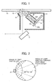
- Fig. 1 is a perspective of the illumination device according to an embodiment of the present invention.
- the illumination device includes an LED 21 and a light guide 22.
- the LED 21 is a wide-directivity type light source.
- the LED 21 is mounted on a board 20.
- a first end surface (entrance surface) 22a of the light guide 22 is in contact with the LED 21, and a second end surface (exit surface) 22b points towards the direction of the light (towards the light-receiving surface).
- the rest of the parts are identical to those shown in Fig. 9 and have been assigned the same reference numerals.
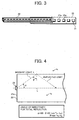
- Fig. 2 is a schematic for explaining an emission distribution of the LED 21, which is of the wide-directivity type.
- the range of light emitted from the emission surface of the LED 21 is 100 degrees to 120 degrees, as shown in Fig. 2.
- Fig. 1 is a cross-sectibnal drawing illustrating a structure in which the light guide 22 guides the light emitted by the LED 21 shown in Fig. 2 towards the light-receiving surface.
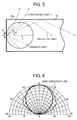
- Fig. 3 is a schematic for explaining the relation between the LEDs 21 and the light guide 22. As shown in Fig. 3, several LEDs 21 are arranged at regular intervals in an array format.
- the light guide 22, which is rectangular in cross-section is disposed along emitting surface 21a of the LED 21, with the exit surface 22b, from which the light emitted by the LED 21 exits, facing the light-receiving surface (the contact glass plate 11).
- the angle at which the light rays do not escape to the atmosphere is decided by the difference in the refractive indices of the atmosphere and the light guide 22.
- the refractive index (n1) of the atmosphere outside of the light guide 22 is 1.0, and the refractive index (n2) of the light guide 22 is approximately 1.52 if the light guide 22 includes an optical glass (crown glass), the angle at which the light rays do not escape to the atmosphere, in other words, the so-called critical angle ⁇ (the angle between the light path and the normal dropped from the point where the light path meets the side surface of the light guide 22 to the side surface of the light guide 22 is given by Expression (1) given below.
- ⁇ sin ⁇ 1 ( n 1 / n 2 )
- the critical angle ⁇ would be 41 degrees and the angle of directivity ⁇ would be 49 degrees.
- those light rays of the light emitted from the LED 21 that have an angle of directivity ( ⁇ ) that is equal to or less than 49 degrees do not escape outside from the side surface of the light guide 22 and are reflected within the light guide 22.
- the light is totally reflected within the light guide 22 and propagated above the LED 21 (along the direction forming an angle of directivity ( ⁇ ) of 0 degrees).
- the light falling in the range of 49 [degrees] ⁇ 2, that is roughly 100 degrees is propagated to the exit surface 22b of the light guide 22.
- the light that falls in the remaining 0 degree to 20 degrees range escapes outside from the side surface of the light guide 22.
- an amount of light that is equal to or greater than 80% of from the LED 21 ends up being propagated towards the exit surface 22b of the light guide 22 if the light guide 22 is made of optical glass (crown glass).
- Fig. 6 is a schematic for explaining the relation between the angle of directivity of the wide-directivity LED 21 and the light intensity.
- the inner thick line represents the standard characteristics of a conventional LED
- the outer thin line represents the characteristics of the wide-directivity LED.
- the angle of directivity ( ⁇ ) is in the vicinity of 45 degrees
- the light intensity is around 0.5 (a relative value obtained by assuming light intensity to be 1.0 when the angle of directivity ( ⁇ ) is 0 degree).
- a concept of a half-value angle ⁇ is introduced for the wide-directivity LED 21 according to the present embodiment.
- the half-value angle ⁇ is the angle of the direction where the light intensity t is half of the maximum light intensity with respect to the direction of the optical axis L.
- the illuminating beam emitted by the LED 21 is totally reflected by a side surface 22c of the light guide 22 before being emitted from the exit surface 22b of the light guide 22.
- Fig. 7 is a schematic for explaining the relation between an interval between the LEDs, the dimension of the light guide in the main scanning direction, which is also the light emission direction, and the angle of directivity.
- the dimension of, i.e., the distance between, the light guide 22 in the direction of light propagation is.A
- the interval, i.e., distance, between adjoining LEDs 21 is B
- ⁇ is tan -1 (B/2A)
- ⁇ can be expressed as, ⁇ ⁇ tan ⁇ 1 ( B / 2 A )
- the dimension of the light guide 22 and the interval between the LEDs 21 in the main scanning direction can be set so that substantially 80% of the light emitted from the LED 21 can be effectively used as the illuminating light.
- ⁇ is given in radians. However, it can be easily converted to degrees.
- the critical angle ⁇ becomes smaller resulting in increase in the half-value angle ⁇ , as the refractive index of the light guide 22 becomes larger. Therefore, the illumination efficiency can be enhanced by employing the light guide 22 made of a material having a large refractive index.
- Optical glass is the material of choice for the light guide 22.
- An optical glass has a homogeneous refractive index and thus is devoid of striae.
- the optical glass used for the light guide 22 is usually crown glass (with a refractive index of 1.5168) known as BK7, flint glass (with a refractive index of 1.6200) known as F2, or heavy flint glass (with a refractive index of 1.7174) known as SF1.
- Material used for optical lens such as acryl resin or polycarbonate resin, which is a transparent resin (having a transmission rate that is equal to or greater than 92%) may also be used as the material for the light guide 22.
- These resin substances have a refractive index of 1.58 to 1.59 and have characteristics that are midway between those of crown glass and flint glass.
- a reflecting unit such as a diffuse reflective plate (white plate, etc.) may be placed on the side surfaces 22c and 22d of the light guide 22, so that the light emitted from the LED 21 does not escape to the outside from the light guide 22.
- Fig. 8 is a perspective of a system as a whole that includes an image forming apparatus according to the present embodiment.
- the system basically includes an image forming apparatus main unit 100, the scanner 200 disposed above the image forming apparatus main unit 100, an automatic document feeder (hereinafter, "ADF") 300 disposed above the scanner 200, a large-capacity paper feeding device 400 disposed to the right of the image forming apparatus main unit 100 in Fig. 8, and a sheet finisher 500 disposed to the left of the image forming apparatus main unit 100 in Fig. 8.
- ADF automatic document feeder
- the image forming apparatus main unit 100 includes an image writer 110, an image forming member 120, a fixing member 130, a reverse side transporting member 140, a paper feeder 150, a vertical transporting member 160, and a manual paper feeder 170.
- the image writer 110 adjusts the light source LED based on the reading of the image data on the original document by the scanner 200 and carries out laser writing on a photosensitive drum 121 by scanning optical system consisting of polygonal mirror, f ⁇ lens, etc.
- the image forming member 120 includes image-forming elements known in electrophotographic method, such as the photosensitive drum 121, a developing unit 122, a transfer unit 123, a cleaning unit 124, and a quenching unit, with the developing unit 122, the transfer unit 123, the cleaning unit 124, and the quenching unit disposed along the outer periphery of the photosensitive drum 121.
- the fixing unit 120 fixes the image transferred by the transfer unit 123 to the recording paper.
- the reverse-side transporting member 140 is located downstream of the fixing member 120 in the sheet transport direction, and includes a first switching pawl 141, a reverse transport path 142 to which the recording paper is guided by the first switching pawl 141, an image forming side transport path 143, and a sheet finisher side transport path 144.
- the first switching pawl 141 switches the sheet transport direction towards the sheet finisher 500 or towards the reverse-side transporting member 140.
- the image forming side transport path 143 transports the recording paper reversed by the reverse transport path 142 again towards the transfer unit 123.
- the sheet finisher side transport path 144 transports the reversed recording paper towards the sheet finisher 500.
- a second switching pawl 145 is located the image forming side transport path 143 and the sheet finisher side transport path 144 branch out.
- the paper feeder 150 is four-tiered, the recording paper of the selected tier being drawn and guided to the vertical transporting member 160 by pick-up rollers and feeding rollers of the tier.
- the vertical transporting member 160 carries the recording paper fed from the any of the tiers of the paper feeder up to a pair of resist rollers 161 located just before the transfer unit 123 upstream in the sheet transport direction.
- the resist rollers 161 feed the recording paper to the transfer unit 123, timing it so that the recording paper is presented at the transfer unit 123 when the leading end of the latent image on the photosensitive drum 121 approaches the recording paper.
- the manual paper feeder 170 includes a manual tray 171, which can be opened or closed whenever required for manually feeding the recording paper. In this case too, the resist rollers 161 feed the recording paper to the transfer unit 123, timing it so that recording paper is presented at the transfer unit when the leading end of the latent image on the photosensitive drum 121 approaches the recording paper.
- the large-capacity paper feeding device 400 can stack a large volume of recording paper of identical size. As the number of sheets of recording paper dwindles in the large-capacity paper feeding device 400, a base rack 402 shifts upward little by little so that a pick-up roller 401 can access the stack to draw a sheet therefrom.
- the vertical transporting member 160 transports the recording paper fed by the pick-up roller 401 up to a nip region of the resist rollers 161.
- the sheet finisher 500 carries out post-processing such as punching, aligning, stapling, separating, etc.
- the sheet finisher 500 is equipped with a punch unit 501, a stapling tray (for aligning the recording papers). 502, a stapler 503, and a shift tray 504.
- the sheets of recording paper transported from the image forming apparatus main unit 100 to the sheet finisher 500 are to be punched, the punch unit 501 punches the recording paper one at a time, and if the recording paper is not marked for any processing, it is ejected to a proof tray 505. Otherwise, the punched sheets of recording paper are ejected to the shift tray 504 for further processing such as sorting, stacking, separating, etc.
- Separating a preceding set of sheets from the following set of sheets is carried out in the present embodiment by shifting the shift tray 504 by a predetermined amount in the direction perpendicular to the sheet transport direction.
- a method involving shifting the sheet in the direction perpendicular to the sheet transport direction in the sheet transport path may also used for separating sets of sheets.
- the sheets of recording paper are guided to a lower transport path 506 and therefrom to the shift tray 504, the rear edge of which aligns the sheets in the direction perpendicular to the sheet transport direction.
- a pair of jogger fences in the shift tray 504 aligns the sheets in the direction parallel to the sheet transport direction.
- a prestack transport path 507 is provided in the lower transport path 506 which stacks several sheets of recording paper while they are being transported, so that image forming operation of the image forming apparatus main unit 100 does not have to be halted for sheet finishing process.
- the scanner 200 has the same structure as that shown in Fig. 9. However, the scanner 200 according to the present invention is equipped with the illumination device shown in Fig. 1.
- the scanner optically scans the original document that is guided to and placed on a contact glass plate 210 by the ADF 300.
- the imaging lens 7 forms a scanned image by the first mirror 2, the second mirror 4, and the third mirror 5.
- the scanned image is read by a photoelectric element such as the CCD 8 or a Complementary Metal Oxide Semiconductor (CMOS).
- CMOS Complementary Metal Oxide Semiconductor
- the image data that is read is subjected to a designated image processing in a hot shown image processing circuit and is held in a storage device: During image formation, the image data is read from the storage device by the image writer 110.
- the image data is optically written by adjusting the amount of light in the aforementioned manner in response to the image data.
- the ADF 300 includes a reverse-side scanning furiction and is mounted on an installation surface of the contact glass plate 210.
- the ADF 300 can be opened or closed manually.
- a wide-directivity LED having a half-value angle that satisfies the aforementioned relation is used. Consequently when the LED is used coupled with a light guide, the amount of light from the LED can be used to the maximum possible extent and a uniform light intensity distribution pattern can be obtained.
Landscapes
- Physics & Mathematics (AREA)
- Optics & Photonics (AREA)
- Engineering & Computer Science (AREA)
- Multimedia (AREA)
- Signal Processing (AREA)
- General Physics & Mathematics (AREA)
- Facsimile Scanning Arrangements (AREA)
- Light Sources And Details Of Projection-Printing Devices (AREA)
Applications Claiming Priority (1)
| Application Number | Priority Date | Filing Date | Title |
|---|---|---|---|
| JP2005057541A JP2006243258A (ja) | 2005-03-02 | 2005-03-02 | 照明装置、画像読み取り装置及び画像形成装置 |
Publications (1)
| Publication Number | Publication Date |
|---|---|
| EP1699224A1 true EP1699224A1 (fr) | 2006-09-06 |
Family
ID=36129662
Family Applications (1)
| Application Number | Title | Priority Date | Filing Date |
|---|---|---|---|
| EP06002507A Ceased EP1699224A1 (fr) | 2005-03-02 | 2006-02-07 | Dispositif d'éclairage, lecteur d'images et appareil de formation d'images |
Country Status (3)
| Country | Link |
|---|---|
| US (1) | US7537367B2 (fr) |
| EP (1) | EP1699224A1 (fr) |
| JP (1) | JP2006243258A (fr) |
Cited By (1)
| Publication number | Priority date | Publication date | Assignee | Title |
|---|---|---|---|---|
| EP2495948A4 (fr) * | 2009-10-30 | 2014-08-20 | Sharp Kk | Dispositif d'éclairage, dispositif de lecture d'image équipé de ce dispositif d'éclairage, et dispositif de formation d'image équipé de ce dispositif de lecture d'image |
Families Citing this family (10)
| Publication number | Priority date | Publication date | Assignee | Title |
|---|---|---|---|---|
| JP4863840B2 (ja) * | 2006-10-27 | 2012-01-25 | 株式会社リコー | 画素形成装置、光走査装置、光走査方法、画像形成装置、カラー画像形成装置 |
| US8081355B2 (en) * | 2007-03-05 | 2011-12-20 | Ricoh Company, Ltd. | Illumination unit, image read apparatus, image formation apparatus |
| US8199371B2 (en) | 2008-02-25 | 2012-06-12 | Ricoh Company, Ltd. | Image reader and image formation apparatus |
| US8169671B2 (en) * | 2008-06-30 | 2012-05-01 | Ricoh Company, Ltd. | Lighting unit, image reading apparatus and image forming apparatus using the same |
| JP4922258B2 (ja) * | 2008-07-14 | 2012-04-25 | 株式会社リコー | 画像読取装置及び画像形成装置 |
| JP5196305B2 (ja) * | 2008-07-30 | 2013-05-15 | 株式会社リコー | 読取光学系ユニット、画像読取装置および画像形成装置 |
| JP2010130056A (ja) * | 2008-11-25 | 2010-06-10 | Ricoh Co Ltd | 光照射装置、画像読取装置および画像形成装置 |
| JP5359370B2 (ja) * | 2009-02-26 | 2013-12-04 | 株式会社リコー | 原稿照明装置並びにそれを用いた画像読取装置 |
| JP5862251B2 (ja) | 2011-12-01 | 2016-02-16 | 株式会社リコー | 光照射装置、画像読取装置および画像形成装置 |
| JP6255313B2 (ja) * | 2014-07-02 | 2017-12-27 | キヤノン・コンポーネンツ株式会社 | イメージセンサユニット、紙葉類識別装置、画像読取装置および画像形成装置 |
Citations (5)
| Publication number | Priority date | Publication date | Assignee | Title |
|---|---|---|---|---|
| US4255042A (en) * | 1979-03-26 | 1981-03-10 | International Business Machines Corporation | Light pipe for accurate erasure of photoconductor charge |
| US4344691A (en) * | 1980-06-23 | 1982-08-17 | International Business Machines Corporation | Zonal concentrator for accurate erasure of photoconductor charge |
| JPH07162586A (ja) * | 1993-12-07 | 1995-06-23 | Matsushita Electric Ind Co Ltd | 発光装置とそれを用いた密着型イメージセンサユニット |
| US6072171A (en) * | 1995-08-24 | 2000-06-06 | Matsushita Electric Industrial Co., Ltd. | Linear illumination device |
| US20030179420A1 (en) * | 2002-03-22 | 2003-09-25 | Kouzou Fujino | Lighting apparatus and image reading apparatus |
Family Cites Families (16)
| Publication number | Priority date | Publication date | Assignee | Title |
|---|---|---|---|---|
| JPS63240167A (ja) * | 1987-03-27 | 1988-10-05 | Canon Inc | 光源装置 |
| JPH03187280A (ja) | 1989-12-18 | 1991-08-15 | Nkk Corp | Bi―Te系熱電変換薄膜及びその熱電変換素子 |
| JP3347338B2 (ja) | 1991-02-19 | 2002-11-20 | ヤマハ株式会社 | 楽音合成装置 |
| JPH07297996A (ja) * | 1994-04-27 | 1995-11-10 | Nippon Sheet Glass Co Ltd | ライン照明装置およびそれを用いた画像読み取り装置 |
| JP3987838B2 (ja) * | 1997-03-04 | 2007-10-10 | 松下電器産業株式会社 | 線状照明装置 |
| JP3682817B2 (ja) * | 1997-05-08 | 2005-08-17 | 株式会社シチズン電子 | 画像読み取り装置の線状光源ユニット |
| EP0879991A3 (fr) * | 1997-05-13 | 1999-04-21 | Matsushita Electric Industrial Co., Ltd. | Système d'illumination |
| JPH11232912A (ja) | 1998-02-16 | 1999-08-27 | Pfu Ltd | Led照明構造 |
| JP2000048616A (ja) | 1998-07-24 | 2000-02-18 | Canon Inc | 導光体、照明装置及びそれを用いた画像読取装置 |
| JP2001109084A (ja) | 1999-10-12 | 2001-04-20 | Canon Inc | 照明装置 |
| JP3392117B2 (ja) | 2000-12-01 | 2003-03-31 | キヤノン株式会社 | 読取装置用導光体及び読取装置 |
| JP2004064146A (ja) * | 2002-07-24 | 2004-02-26 | Toshiba Corp | 導光体、ライン照明装置及び画像入力装置 |
| JP4170818B2 (ja) * | 2003-04-11 | 2008-10-22 | 株式会社リコー | 照明装置・原稿読み取り装置・画像形成装置 |
| EP1511289B1 (fr) | 2003-08-19 | 2011-11-23 | Ricoh Company, Ltd. | Dispositif d'éclairage, dispositif de lecture d'images et dispositif de formation d'images |
| JP4157832B2 (ja) | 2003-11-20 | 2008-10-01 | 株式会社リコー | 原稿サイズ検知方法及び原稿読取装置及び画像形成装置 |
| JP3766422B2 (ja) * | 2004-01-13 | 2006-04-12 | ローム株式会社 | 線状光源装置および画像読み取り装置 |
-
2005
- 2005-03-02 JP JP2005057541A patent/JP2006243258A/ja active Pending
-
2006
- 2006-02-02 US US11/345,485 patent/US7537367B2/en active Active
- 2006-02-07 EP EP06002507A patent/EP1699224A1/fr not_active Ceased
Patent Citations (5)
| Publication number | Priority date | Publication date | Assignee | Title |
|---|---|---|---|---|
| US4255042A (en) * | 1979-03-26 | 1981-03-10 | International Business Machines Corporation | Light pipe for accurate erasure of photoconductor charge |
| US4344691A (en) * | 1980-06-23 | 1982-08-17 | International Business Machines Corporation | Zonal concentrator for accurate erasure of photoconductor charge |
| JPH07162586A (ja) * | 1993-12-07 | 1995-06-23 | Matsushita Electric Ind Co Ltd | 発光装置とそれを用いた密着型イメージセンサユニット |
| US6072171A (en) * | 1995-08-24 | 2000-06-06 | Matsushita Electric Industrial Co., Ltd. | Linear illumination device |
| US20030179420A1 (en) * | 2002-03-22 | 2003-09-25 | Kouzou Fujino | Lighting apparatus and image reading apparatus |
Non-Patent Citations (1)
| Title |
|---|
| PATENT ABSTRACTS OF JAPAN vol. 1995, no. 09 31 October 1995 (1995-10-31) * |
Cited By (2)
| Publication number | Priority date | Publication date | Assignee | Title |
|---|---|---|---|---|
| EP2495948A4 (fr) * | 2009-10-30 | 2014-08-20 | Sharp Kk | Dispositif d'éclairage, dispositif de lecture d'image équipé de ce dispositif d'éclairage, et dispositif de formation d'image équipé de ce dispositif de lecture d'image |
| EP3349427A3 (fr) * | 2009-10-30 | 2018-09-05 | Sharp Kabushiki Kaisha | Dispositif d'éclairage, appareil de lecture d'image comprenant le dispositif d'éclairage et appareil de formation d'image comprenant l'appareil de lecture d'image |
Also Published As
| Publication number | Publication date |
|---|---|
| US20060197822A1 (en) | 2006-09-07 |
| US7537367B2 (en) | 2009-05-26 |
| JP2006243258A (ja) | 2006-09-14 |
Similar Documents
| Publication | Publication Date | Title |
|---|---|---|
| US7042599B2 (en) | Image sensor and image reading apparatus | |
| JP5299660B2 (ja) | 照明装置、画像読取装置、及び、画像形成装置 | |
| EP2365688B1 (fr) | Dispositif de lecture d'images | |
| US5463451A (en) | Document reproduction system including a duplex document handler with natural inversion | |
| US8167475B2 (en) | Linear lighting apparatus and image reader using the same | |
| US6565248B2 (en) | Light guide, line illumination apparatus, and image acquisition system | |
| EP2557769A1 (fr) | Unité de capteur d'image et appareil de lecture d'image | |
| US8837015B2 (en) | Illuminator and image reading device and image forming apparatus having the same | |
| EP0887993B1 (fr) | Réseau de lentilles barreaux et appareil de lecture d'image et système les utilisant | |
| US7537367B2 (en) | Illumination device, image reading device, and image forming apparatus | |
| KR101354558B1 (ko) | 화상 판독 장치 및 화상 형성 장치 | |
| KR20140048958A (ko) | 이미지 센서 유닛 및 이것을 사용한 화상 판독 장치 | |
| EP3349427A2 (fr) | Dispositif d'éclairage, appareil de lecture d'image comprenant le dispositif d'éclairage et appareil de formation d'image comprenant l'appareil de lecture d'image | |
| US8446646B2 (en) | Light guide and image reading apparatus | |
| JP2006227384A (ja) | 画像読み取り装置、画像形成装置および画像読み取り方法 | |
| JP2008172562A (ja) | 照明装置、画像読取装置、画像形成装置 | |
| JP2007005860A (ja) | 光照射ユニット、画像読取機構、画像読取装置及び画像形成装置 | |
| JP5146798B2 (ja) | 照明装置、画像読取装置、画像形成装置 | |
| JP2008172561A (ja) | 照明装置、画像読取装置及び画像形成装置 | |
| EP1950945B1 (fr) | Élément optique pour illuminateur de document | |
| US7450277B2 (en) | Single pass duplex document path for a digital scanner | |
| US7760434B2 (en) | Document illuminator with surface lens | |
| US20240103222A1 (en) | Diffusing member, illuminating device, image reading apparatus, and image forming apparatus | |
| JP5712046B2 (ja) | 照明装置、画像読み取り装置及び画像形成装置 | |
| JP2014161058A (ja) | 照明装置、画像読み取り装置及び画像形成装置 |
Legal Events
| Date | Code | Title | Description |
|---|---|---|---|
| PUAI | Public reference made under article 153(3) epc to a published international application that has entered the european phase |
Free format text: ORIGINAL CODE: 0009012 |
|
| AK | Designated contracting states |
Kind code of ref document: A1 Designated state(s): AT BE BG CH CY CZ DE DK EE ES FI FR GB GR HU IE IS IT LI LT LU LV MC NL PL PT RO SE SI SK TR |
|
| AX | Request for extension of the european patent |
Extension state: AL BA HR MK YU |
|
| 17P | Request for examination filed |
Effective date: 20061109 |
|
| AKX | Designation fees paid |
Designated state(s): DE ES FR GB IT NL |
|
| 17Q | First examination report despatched |
Effective date: 20080527 |
|
| STAA | Information on the status of an ep patent application or granted ep patent |
Free format text: STATUS: THE APPLICATION HAS BEEN REFUSED |
|
| 18R | Application refused |
Effective date: 20090929 |