EP1699228A1 - Module de caméra et son procédé de fabrication - Google Patents
Module de caméra et son procédé de fabrication Download PDFInfo
- Publication number
- EP1699228A1 EP1699228A1 EP05022788A EP05022788A EP1699228A1 EP 1699228 A1 EP1699228 A1 EP 1699228A1 EP 05022788 A EP05022788 A EP 05022788A EP 05022788 A EP05022788 A EP 05022788A EP 1699228 A1 EP1699228 A1 EP 1699228A1
- Authority
- EP
- European Patent Office
- Prior art keywords
- lens
- camera module
- lens holder
- surface mount
- mount device
- Prior art date
- Legal status (The legal status is an assumption and is not a legal conclusion. Google has not performed a legal analysis and makes no representation as to the accuracy of the status listed.)
- Granted
Links
- 238000004519 manufacturing process Methods 0.000 title claims abstract description 10
- 239000000463 material Substances 0.000 claims abstract description 16
- 238000000034 method Methods 0.000 claims abstract description 8
- 229910000679 solder Inorganic materials 0.000 claims description 6
- 229920000106 Liquid crystal polymer Polymers 0.000 claims description 5
- 239000004977 Liquid-crystal polymers (LCPs) Substances 0.000 claims description 5
- 239000004677 Nylon Substances 0.000 claims description 3
- 239000000919 ceramic Substances 0.000 claims description 3
- 239000011521 glass Substances 0.000 claims description 3
- 229920001778 nylon Polymers 0.000 claims description 3
- 238000005476 soldering Methods 0.000 abstract description 13
- 238000012544 monitoring process Methods 0.000 description 2
- 238000012856 packing Methods 0.000 description 2
- 230000003068 static effect Effects 0.000 description 2
- 238000012986 modification Methods 0.000 description 1
- 230000004048 modification Effects 0.000 description 1
- 230000000087 stabilizing effect Effects 0.000 description 1
Images


Classifications
-
- H—ELECTRICITY
- H04—ELECTRIC COMMUNICATION TECHNIQUE
- H04N—PICTORIAL COMMUNICATION, e.g. TELEVISION
- H04N23/00—Cameras or camera modules comprising electronic image sensors; Control thereof
- H04N23/50—Constructional details
- H04N23/55—Optical parts specially adapted for electronic image sensors; Mounting thereof
Definitions
- the present invention relates to a camera module, and more particularly, to a high heatproof camera module.
- a wide variety of audio and video information is now widely available in digital formats.
- An important device for the inputting and outputting of such information is the camera module. Because of its applicability in a broad array of fields, from small devices such as mobile phones, personal digital assistants (PDAs) to large devices such as large digital video cameras (including monitor systems), the digital camera module is becoming more and more useful.
- PDAs personal digital assistants
- large digital video cameras including monitor systems
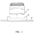
- a socket 13 is usually required to connect the camera module 11 with the main board 12.
- the mobile phone, laptop computer, digital camera, or digital video camera, etc. is provided the functionality of a camera, and is able to provide static photographs, or even dynamic monitoring (such as a rear-view monitor for backing up a car).
- the traditional camera module 11 is not heatproof, and so surface mount technology (SMT), which uses high-heat soldering equipment, cannot be used to assemble the camera module 11 with the main board 12. As a result, the traditional camera module 11 may be not provided for SMT assembly process and neither to achieve mass production.
- SMT surface mount technology
- the present invention discloses a high heatproof camera module and a related manufacturing process thereof, which employs surface mount technology to directly bond the camera module onto a main board of a system.
- the present invention provides a camera module comprising a lens, a lens holder, the lens and the lens holder engaged with each other, and an image sensor board located under the lens holder.
- the lens is formed from a highly heatproof material, preferably sustaining with more than 180 ⁇ -the high temperature requirements of SMT soldering equipment.
- the highly heatproof material of the lens may be a ceramic, a highly heatproof glass, or the like.
- the lens holder is formed of a highly heatproof material, such as liquid crystal polymer (LCP), nylon, or the like.
- the image sensor board is typically made by SMT, so it can sustain the high temperatures of SMT soldering equipment.
- the present invention also provides a manufacturing process for a camera module that comprises: providing a lens; engaging the lens with a lens holder; fixing an image sensor board onto a bottom of the holder; and combining the lens, the lens holder, and the image sensor board to form a surface mount device (SMD).
- a manufacturing process for a camera module comprises: providing a lens; engaging the lens with a lens holder; fixing an image sensor board onto a bottom of the holder; and combining the lens, the lens holder, and the image sensor board to form a surface mount device (SMD).
- SMD surface mount device
- step of forming the SMD before the step of forming the SMD, further comprises the step of adjusting the lens to substantially provide focus.
- the step of forming the SMD may further comprise the step of mounting solder balls on the SMD or applying solder on a surface of the SMD.
- FIG 2 shows an exploded view of a camera module 2 according to the present invention.
- the camera module 2 of this invention comprises a lens 21, a lens holder 22, and an image sensor board 23.
- the lens 21 and the lens holder 22 are engaged with each other.
- the image sensor board 23 is located under the lens holder 22 for the forming of an image. By adjusting the lens 21, the best focus of the camera module 2 can be reached.
- the engagement of the lens 21 and the holder 22 may be adapted by outer threads 210 of the lens 21 and inner threads 220 of the holder 22. Additionally, the engagement of the threads 210 and 220 can make the lens 21 movable; therefore, by moving the lens 21 to adjust the focus, the best focus of the camera module 2 can be reached.
- the lens 21 of the present invention is formed of a highly heatproof material.
- the highly heatproof material can sustain temperatures in excess of 1800, such as the high temperatures of SMT soldering equipment (the typical temperature of soldering equipment is between about 180 ⁇ and 240 ⁇ ).
- the material of the lens 21 may be, for example, ceramic, highly heatproof glass, or other such materials.
- the lens holder 22 of this invention is also required to sustain the high temperatures (i.e., in excess of 180 ⁇ ) of SMT soldering equipment, it is also formed from a highly heatproof material, such as liquid crystal polymer (LCP), nylon, or the like.
- LCP liquid crystal polymer
- the lens 21 and the lens holder 22 are respectively formed from highly heatproof materials that are able to withstand the high temperatures of SMT soldering equipment.
- the image sensor board 23 is made by SMT, so it is also able to sustain the high temperatures of SMT soldering equipment.
- the camera module 2 consequently is able to sustain the high temperatures of SMT soldering equipment.
- the camera module 2 another embodiment of this invention, can be mounted onto a main board 3 of a system, such as a mobile phone system, a laptop computer system, a digital camera system, a digital video system, or the like.
- the system e.g.
- a mobile phone, a laptop computer, a digital camera, a digital video, etc. is provided with camera-related functionalities. These functionalities include not only the static functions of still photography, but also dynamic monitoring, such as rear-view monitors for backing up a car.
- the camera module 2 of this invention can sustain the high temperatures of SMT soldering equipment, enabling system manufacturers to bond the camera module 2 onto the main board 3 by surface mount technology, which thus enables production automation.
- step S51 provides a lens 21.
- step 52 the lens 21 is engaged with a lens holder 22, as described above, the engagement of the lens 21 and the lens holder 22 may be adapted by outer threads 210 of the lens 21 and inner threads 220 of the holder 22.
- step S53 an image sensor board 3 is fixed onto a bottom of the lens holder 22.
- the lens 21 may need to be adjusted to pre-focus by a calibration tool (not shown), and thus the process of this invention also provides a step for the focusing of the lens 21, as shown in step S54.
- the camera module 2 may be adjusted with a calibration tool to provide the appropriate focus by moving the lens 21 and the lens holder 22, and then stabilizing the best-focus position.
- a surface mount device (SMD) of the camera module 2 is formed by combining the lens 21, the lens holder 22, and the image sensor board 23.
- the SMD of the camera module 2 can be adapted for bonding onto a main board 3 of a system, such as a mobile phone system, a laptop computer system, a digital camera system, a digital video system, or the like, with an SMT machine (not shown).
- a system such as a mobile phone system, a laptop computer system, a digital camera system, a digital video system, or the like.
- the step of forming the SMD may further comprise a step of mounting solder balls onto the SMD, or applying solder onto a surface of the SMD, as indicated in step S56.
- step S57 the SMD of camera module 2 is bonded onto the main board 3 by surface mount technology.
- This invention may further comprise the step of packing the SMD of camera module 2, such as packing the SMD of camera module 2 in a tube or a roll, according to the SMT machine. Because this invention utilizes highly heatproof materials, it can be used in SMT machines for more efficient mass production. Additionally, the present invention can reduce costs associated with the socket 13, as depicted in FIG 1, between the traditional camera module 11 and main board 12.
Landscapes
- Engineering & Computer Science (AREA)
- Multimedia (AREA)
- Signal Processing (AREA)
- Studio Devices (AREA)
- Lens Barrels (AREA)
Applications Claiming Priority (1)
| Application Number | Priority Date | Filing Date | Title |
|---|---|---|---|
| CNA2005100531618A CN1828354A (zh) | 2005-03-04 | 2005-03-04 | 照相机模块及其制备方法 |
Publications (2)
| Publication Number | Publication Date |
|---|---|
| EP1699228A1 true EP1699228A1 (fr) | 2006-09-06 |
| EP1699228B1 EP1699228B1 (fr) | 2008-12-17 |
Family
ID=36178230
Family Applications (1)
| Application Number | Title | Priority Date | Filing Date |
|---|---|---|---|
| EP05022788A Expired - Lifetime EP1699228B1 (fr) | 2005-03-04 | 2005-10-19 | Module de caméra et son procédé de fabrication |
Country Status (3)
| Country | Link |
|---|---|
| EP (1) | EP1699228B1 (fr) |
| CN (1) | CN1828354A (fr) |
| DE (1) | DE602005011751D1 (fr) |
Cited By (12)
| Publication number | Priority date | Publication date | Assignee | Title |
|---|---|---|---|---|
| US9284435B2 (en) | 2012-10-16 | 2016-03-15 | Ticona Llc | Antistatic liquid crystalline polymer composition |
| US9355753B2 (en) | 2012-12-05 | 2016-05-31 | Ticona Llc | Conductive liquid crystalline polymer composition |
| US9512293B2 (en) | 2013-03-13 | 2016-12-06 | Ticona Llc | Antistatic liquid crystalline polymer composition |
| US9822254B2 (en) | 2014-04-09 | 2017-11-21 | Ticona Llc | Camera module |
| US10287421B2 (en) | 2014-04-09 | 2019-05-14 | Ticona Llc | Antistatic polymer composition |
| US10829634B2 (en) | 2017-12-05 | 2020-11-10 | Ticona Llc | Aromatic polymer composition for use in a camera module |
| US11702539B2 (en) | 2020-02-26 | 2023-07-18 | Ticona Llc | Polymer composition for an electronic device |
| US11715579B2 (en) | 2020-02-26 | 2023-08-01 | Ticona Llc | Electronic device |
| US11728065B2 (en) | 2020-07-28 | 2023-08-15 | Ticona Llc | Molded interconnect device |
| US11729908B2 (en) | 2020-02-26 | 2023-08-15 | Ticona Llc | Circuit structure |
| US12247116B2 (en) | 2021-12-01 | 2025-03-11 | Ticona Llc | Antenna module |
| US12522716B2 (en) | 2020-02-26 | 2026-01-13 | Ticona Llc | Electronic device |
Families Citing this family (1)
| Publication number | Priority date | Publication date | Assignee | Title |
|---|---|---|---|---|
| CN102116918B (zh) * | 2009-12-30 | 2013-08-28 | 鸿富锦精密工业(深圳)有限公司 | 镜头模组的制备方法 |
Citations (6)
| Publication number | Priority date | Publication date | Assignee | Title |
|---|---|---|---|---|
| EP0978251A1 (fr) * | 1998-08-07 | 2000-02-09 | Olympus Optical Co., Ltd. | Endoscope pouvant être passé à l'autoclave |
| EP1347637A2 (fr) * | 2002-03-22 | 2003-09-24 | Konica Corporation | Dispositif de prise de vues |
| US6734419B1 (en) * | 2001-06-28 | 2004-05-11 | Amkor Technology, Inc. | Method for forming an image sensor package with vision die in lens housing |
| EP1465411A2 (fr) * | 2003-03-31 | 2004-10-06 | Mitsumi Electric Co., Ltd. | Module compact de caméra |
| WO2004107437A1 (fr) * | 2003-05-30 | 2004-12-09 | Valen Technologies (S) Pte Ltd | Module de detection d'image et son procede de construction |
| US20040263680A1 (en) * | 2003-06-30 | 2004-12-30 | Elazer Sonnenschein | Autoclavable imager assembly |
-
2005
- 2005-03-04 CN CNA2005100531618A patent/CN1828354A/zh active Pending
- 2005-10-19 DE DE602005011751T patent/DE602005011751D1/de not_active Expired - Lifetime
- 2005-10-19 EP EP05022788A patent/EP1699228B1/fr not_active Expired - Lifetime
Patent Citations (6)
| Publication number | Priority date | Publication date | Assignee | Title |
|---|---|---|---|---|
| EP0978251A1 (fr) * | 1998-08-07 | 2000-02-09 | Olympus Optical Co., Ltd. | Endoscope pouvant être passé à l'autoclave |
| US6734419B1 (en) * | 2001-06-28 | 2004-05-11 | Amkor Technology, Inc. | Method for forming an image sensor package with vision die in lens housing |
| EP1347637A2 (fr) * | 2002-03-22 | 2003-09-24 | Konica Corporation | Dispositif de prise de vues |
| EP1465411A2 (fr) * | 2003-03-31 | 2004-10-06 | Mitsumi Electric Co., Ltd. | Module compact de caméra |
| WO2004107437A1 (fr) * | 2003-05-30 | 2004-12-09 | Valen Technologies (S) Pte Ltd | Module de detection d'image et son procede de construction |
| US20040263680A1 (en) * | 2003-06-30 | 2004-12-30 | Elazer Sonnenschein | Autoclavable imager assembly |
Cited By (24)
| Publication number | Priority date | Publication date | Assignee | Title |
|---|---|---|---|---|
| US9988519B2 (en) | 2012-10-16 | 2018-06-05 | Ticona Llc | Antistatic liquid crystalline polymer composition |
| US9284435B2 (en) | 2012-10-16 | 2016-03-15 | Ticona Llc | Antistatic liquid crystalline polymer composition |
| US9355753B2 (en) | 2012-12-05 | 2016-05-31 | Ticona Llc | Conductive liquid crystalline polymer composition |
| US10941275B2 (en) | 2013-03-13 | 2021-03-09 | Ticona Llc | Compact camera module |
| US9512293B2 (en) | 2013-03-13 | 2016-12-06 | Ticona Llc | Antistatic liquid crystalline polymer composition |
| US11884795B2 (en) | 2013-03-13 | 2024-01-30 | Ticona Llc | Liquid crystalline polymer composition |
| US10280282B2 (en) | 2013-03-13 | 2019-05-07 | Ticona Llc | Compact camera module |
| US11725095B2 (en) | 2013-03-13 | 2023-08-15 | Ticona Llc | Compact camera module |
| US11136445B2 (en) | 2013-03-13 | 2021-10-05 | Ticona Llc | Liquid crystalline polymer composition |
| US10287421B2 (en) | 2014-04-09 | 2019-05-14 | Ticona Llc | Antistatic polymer composition |
| US9822254B2 (en) | 2014-04-09 | 2017-11-21 | Ticona Llc | Camera module |
| US11208556B2 (en) | 2014-04-09 | 2021-12-28 | Ticona Llc | Camera module |
| US12163023B2 (en) | 2014-04-09 | 2024-12-10 | Ticona Llc | Camera module |
| US10640648B2 (en) | 2014-04-09 | 2020-05-05 | Ticona Llc | Camera module |
| US10829634B2 (en) | 2017-12-05 | 2020-11-10 | Ticona Llc | Aromatic polymer composition for use in a camera module |
| US11725106B2 (en) | 2017-12-05 | 2023-08-15 | Ticona Llc | Aromatic polymer composition for use in a camera module |
| US12035467B2 (en) | 2020-02-26 | 2024-07-09 | Ticona Llc | Circuit structure |
| US11729908B2 (en) | 2020-02-26 | 2023-08-15 | Ticona Llc | Circuit structure |
| US11715579B2 (en) | 2020-02-26 | 2023-08-01 | Ticona Llc | Electronic device |
| US11702539B2 (en) | 2020-02-26 | 2023-07-18 | Ticona Llc | Polymer composition for an electronic device |
| US12297348B2 (en) | 2020-02-26 | 2025-05-13 | Ticona Llc | Polymer composition for an electronic device |
| US12522716B2 (en) | 2020-02-26 | 2026-01-13 | Ticona Llc | Electronic device |
| US11728065B2 (en) | 2020-07-28 | 2023-08-15 | Ticona Llc | Molded interconnect device |
| US12247116B2 (en) | 2021-12-01 | 2025-03-11 | Ticona Llc | Antenna module |
Also Published As
| Publication number | Publication date |
|---|---|
| CN1828354A (zh) | 2006-09-06 |
| EP1699228B1 (fr) | 2008-12-17 |
| DE602005011751D1 (de) | 2009-01-29 |
Similar Documents
| Publication | Publication Date | Title |
|---|---|---|
| US20060197862A1 (en) | Camera module and the manufacturing process thereof | |
| US9004132B2 (en) | Apparatus and method for manufacturing camera module | |
| EP1699228A1 (fr) | Module de caméra et son procédé de fabrication | |
| US20080122967A1 (en) | Digital camera module and method for assembling the same | |
| US20080142917A1 (en) | Image sensor module, method of manufacturing the same, and camera module having the same | |
| JPH10321827A (ja) | 撮像装置及びカメラ | |
| CN101432759A (zh) | 在柔性衬底上安装图像记录装置的系统和方法 | |
| CA2625587A1 (fr) | Module de camera monte sur une tranche et procede de fabrication de ce module | |
| JP2005533452A (ja) | カメラモジュール、カメラシステム及びカメラモジュールの製造方法 | |
| JP2015176151A (ja) | レンズモジュール位置決め構造 | |
| CN107155028A (zh) | 成像模组及电子装置 | |
| KR20230006426A (ko) | 카메라 모듈 | |
| CN205545560U (zh) | 成像模组及电子装置 | |
| CN107155048A (zh) | 双摄像头模组及终端设备 | |
| CN206181192U (zh) | 摄像头模组 | |
| JP2008172724A (ja) | カメラモジュール、台座マウント、撮像装置及び撮像装置の製造方法 | |
| US10200578B2 (en) | Camera device and electronic device with the same | |
| US10756448B2 (en) | Camera module facilitating industrialized assembly line and electronic device with the same | |
| WO2022151806A1 (fr) | Ensemble caméra et appareil électronique | |
| JP2006080961A (ja) | 撮像装置及び該撮像装置を備えた携帯端末 | |
| US20200271885A1 (en) | Lens module and electronic device using the lens module | |
| US7782388B2 (en) | Solid image pickup unit and camera module | |
| CN205545578U (zh) | 成像模组及电子装置 | |
| JP2007150708A (ja) | 撮像モジュールおよび撮像装置 | |
| KR20130040425A (ko) | 표면 실장형 카메라 모듈 패키지 |
Legal Events
| Date | Code | Title | Description |
|---|---|---|---|
| PUAI | Public reference made under article 153(3) epc to a published international application that has entered the european phase |
Free format text: ORIGINAL CODE: 0009012 |
|
| AK | Designated contracting states |
Kind code of ref document: A1 Designated state(s): AT BE BG CH CY CZ DE DK EE ES FI FR GB GR HU IE IS IT LI LT LU LV MC NL PL PT RO SE SI SK TR |
|
| AX | Request for extension of the european patent |
Extension state: AL BA HR MK YU |
|
| 17P | Request for examination filed |
Effective date: 20060927 |
|
| 17Q | First examination report despatched |
Effective date: 20070129 |
|
| AKX | Designation fees paid |
Designated state(s): DE FI FR GB |
|
| GRAP | Despatch of communication of intention to grant a patent |
Free format text: ORIGINAL CODE: EPIDOSNIGR1 |
|
| GRAS | Grant fee paid |
Free format text: ORIGINAL CODE: EPIDOSNIGR3 |
|
| GRAA | (expected) grant |
Free format text: ORIGINAL CODE: 0009210 |
|
| AK | Designated contracting states |
Kind code of ref document: B1 Designated state(s): DE FI FR GB |
|
| REG | Reference to a national code |
Ref country code: GB Ref legal event code: FG4D |
|
| REF | Corresponds to: |
Ref document number: 602005011751 Country of ref document: DE Date of ref document: 20090129 Kind code of ref document: P |
|
| REG | Reference to a national code |
Ref country code: GB Ref legal event code: 732E Free format text: REGISTERED BETWEEN 20090820 AND 20090826 |
|
| PLBE | No opposition filed within time limit |
Free format text: ORIGINAL CODE: 0009261 |
|
| STAA | Information on the status of an ep patent application or granted ep patent |
Free format text: STATUS: NO OPPOSITION FILED WITHIN TIME LIMIT |
|
| 26N | No opposition filed |
Effective date: 20090918 |
|
| REG | Reference to a national code |
Ref country code: FR Ref legal event code: TP |
|
| PGFP | Annual fee paid to national office [announced via postgrant information from national office to epo] |
Ref country code: DE Payment date: 20101022 Year of fee payment: 6 |
|
| PGFP | Annual fee paid to national office [announced via postgrant information from national office to epo] |
Ref country code: GB Payment date: 20101025 Year of fee payment: 6 |
|
| PGFP | Annual fee paid to national office [announced via postgrant information from national office to epo] |
Ref country code: FR Payment date: 20111118 Year of fee payment: 7 |
|
| GBPC | Gb: european patent ceased through non-payment of renewal fee |
Effective date: 20121019 |
|
| REG | Reference to a national code |
Ref country code: FR Ref legal event code: ST Effective date: 20130628 |
|
| PG25 | Lapsed in a contracting state [announced via postgrant information from national office to epo] |
Ref country code: DE Free format text: LAPSE BECAUSE OF NON-PAYMENT OF DUE FEES Effective date: 20130501 Ref country code: GB Free format text: LAPSE BECAUSE OF NON-PAYMENT OF DUE FEES Effective date: 20121019 |
|
| REG | Reference to a national code |
Ref country code: DE Ref legal event code: R119 Ref document number: 602005011751 Country of ref document: DE Effective date: 20130501 |
|
| PG25 | Lapsed in a contracting state [announced via postgrant information from national office to epo] |
Ref country code: FR Free format text: LAPSE BECAUSE OF NON-PAYMENT OF DUE FEES Effective date: 20121031 |
|
| PGFP | Annual fee paid to national office [announced via postgrant information from national office to epo] |
Ref country code: FI Payment date: 20151027 Year of fee payment: 11 |
|
| PG25 | Lapsed in a contracting state [announced via postgrant information from national office to epo] |
Ref country code: FI Free format text: LAPSE BECAUSE OF NON-PAYMENT OF DUE FEES Effective date: 20161019 |