EP1701435A1 - Stromquellenschaltung, mehrphasen-ansteuerschaltung, stromquellen-schaltungsentwurfverfahren - Google Patents
Stromquellenschaltung, mehrphasen-ansteuerschaltung, stromquellen-schaltungsentwurfverfahren Download PDFInfo
- Publication number
- EP1701435A1 EP1701435A1 EP04807091A EP04807091A EP1701435A1 EP 1701435 A1 EP1701435 A1 EP 1701435A1 EP 04807091 A EP04807091 A EP 04807091A EP 04807091 A EP04807091 A EP 04807091A EP 1701435 A1 EP1701435 A1 EP 1701435A1
- Authority
- EP
- European Patent Office
- Prior art keywords
- voltage
- losses
- value
- inverter
- breakdown
- Prior art date
- Legal status (The legal status is an assumption and is not a legal conclusion. Google has not performed a legal analysis and makes no representation as to the accuracy of the status listed.)
- Withdrawn
Links
Images


Classifications
-
- H—ELECTRICITY
- H02—GENERATION; CONVERSION OR DISTRIBUTION OF ELECTRIC POWER
- H02M—APPARATUS FOR CONVERSION BETWEEN AC AND AC, BETWEEN AC AND DC, OR BETWEEN DC AND DC, AND FOR USE WITH MAINS OR SIMILAR POWER SUPPLY SYSTEMS; CONVERSION OF DC OR AC INPUT POWER INTO SURGE OUTPUT POWER; CONTROL OR REGULATION THEREOF
- H02M1/00—Details of apparatus for conversion
- H02M1/08—Circuits specially adapted for the generation of control voltages for semiconductor devices incorporated in static converters
- H02M1/084—Circuits specially adapted for the generation of control voltages for semiconductor devices incorporated in static converters using a control circuit common to several phases of a multi-phase system
-
- H—ELECTRICITY
- H02—GENERATION; CONVERSION OR DISTRIBUTION OF ELECTRIC POWER
- H02M—APPARATUS FOR CONVERSION BETWEEN AC AND AC, BETWEEN AC AND DC, OR BETWEEN DC AND DC, AND FOR USE WITH MAINS OR SIMILAR POWER SUPPLY SYSTEMS; CONVERSION OF DC OR AC INPUT POWER INTO SURGE OUTPUT POWER; CONTROL OR REGULATION THEREOF
- H02M7/00—Conversion of AC power input into DC power output; Conversion of DC power input into AC power output
- H02M7/42—Conversion of DC power input into AC power output without possibility of reversal
- H02M7/44—Conversion of DC power input into AC power output without possibility of reversal by static converters
- H02M7/48—Conversion of DC power input into AC power output without possibility of reversal by static converters using discharge tubes with control electrode or semiconductor devices with control electrode
-
- H—ELECTRICITY
- H02—GENERATION; CONVERSION OR DISTRIBUTION OF ELECTRIC POWER
- H02M—APPARATUS FOR CONVERSION BETWEEN AC AND AC, BETWEEN AC AND DC, OR BETWEEN DC AND DC, AND FOR USE WITH MAINS OR SIMILAR POWER SUPPLY SYSTEMS; CONVERSION OF DC OR AC INPUT POWER INTO SURGE OUTPUT POWER; CONTROL OR REGULATION THEREOF
- H02M1/00—Details of apparatus for conversion
- H02M1/0048—Circuits or arrangements for reducing losses
-
- Y—GENERAL TAGGING OF NEW TECHNOLOGICAL DEVELOPMENTS; GENERAL TAGGING OF CROSS-SECTIONAL TECHNOLOGIES SPANNING OVER SEVERAL SECTIONS OF THE IPC; TECHNICAL SUBJECTS COVERED BY FORMER USPC CROSS-REFERENCE ART COLLECTIONS [XRACs] AND DIGESTS
- Y02—TECHNOLOGIES OR APPLICATIONS FOR MITIGATION OR ADAPTATION AGAINST CLIMATE CHANGE
- Y02B—CLIMATE CHANGE MITIGATION TECHNOLOGIES RELATED TO BUILDINGS, e.g. HOUSING, HOUSE APPLIANCES OR RELATED END-USER APPLICATIONS
- Y02B70/00—Technologies for an efficient end-user side electric power management and consumption
- Y02B70/10—Technologies improving the efficiency by using switched-mode power supplies [SMPS], i.e. efficient power electronics conversion e.g. power factor correction or reduction of losses in power supplies or efficient standby modes
Definitions
- the present invention relates to techniques for supplying polyphase current.
- Fig. 12 is a circuit diagram illustrating a conventional current-supplying technique.
- a diode bridge 21 applied with an AC voltage having an effective value of 200 V from an AC power supply 1, or a single-phase 200 V power supply, performs full-wave rectification, and provides an inverter 41 with a DC voltage Vdc via a smoothing circuit 31.
- the inverter 41 includes series connection of two IGBT (Insulated Gate Bipolar Transistor) elements having a breakdown voltage of 600 V for each phase, and outputs an AC current of each phase from a node of the series connection to a three-phase motor M1.
- IGBT Insulated Gate Bipolar Transistor
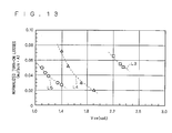
- Fig. 13 shows the relationship between turn-on losses and a saturation voltage Vce(sat) across a collector and an emitter in regard to third-generation, fourth-generation, and fifth-generation IGBT elements having a breakdown voltage of 600 V, as graphs L3, L4, and L5, respectively.
- the turn-on losses are normalized in terms of the number of pulses and current. It is shown that although a tradeoff exists between their characteristic values, both of the characteristic values decrease with each new generation.
- Patent document 1 discloses a technique for controlling a motor used in an air conditioner or a cooling device.
- Patent document 2 discloses a technique for modularizing an inverter unit and a converter unit.
- Non-Patent Document 1 Satoshi Mori, "Latest IPM Technique and Application Examples Thereof", text of 13th technical seminar of Japan Society of Power Electronics, p38 (1998 )
- Non-Patent Document 2 Noriyuki Iwamuro, Tadashi Miyasaka, Yasukazu Seki, "Technical Innovation in U-series IGBT Module", Fuji Electric Journal, vol. 75, No10, p555 (2002 )
- Non-Patent Document 3 Junji Yamada, et al., "Low Turn-Off Switching Energy 1200V IGBT Module” [online], IEEE, [searched October 8, 2003], Internet ⁇ URL:http://www.ineltron.de/english/Low_turn_off_5th_genIGBT.pdf>
- Non-Patent Document 4 " Guide to Practical Use of Mitsubishi Power Module MOS” p46, [online], Mitsubishi Electric, [searched October 8, 2003], Internet ⁇ URL:http://semicon.melco.co.jp/semicon/html/pdf/ka0350a3, pdf>
- Patent Document 1 Japanese Patent Application Laid-Open No. 60-249895
- Patent Document 2 Japanese Patent Application Laid-Open No. 2003-143871
- the present invention has an object to provide a technique for reducing losses in a current supply circuit including an inverter having an IGBT element.
- a current supply circuit includes a voltage doubler rectifying circuit (22) connected to an AC 200 V system power supply (1), and a polyphase inverter circuit (42) including series connection of two switching elements having a breakdown voltage of 1200 V for each phase, and outputting an AC current of each phase from a node of the series connection.
- the switching element is an IGBT element, for example.
- the voltage doubler rectifying circuit and the polyphase inverter circuit are modularized.
- a polyphase drive circuit according to the invention includes the current supply circuit according to the invention, and a polyphase motor for 400 V (M2) supplied with current from the polyphase inverter circuit.
- a method of designing a current supply circuit according to the invention is a method of designing a current supply circuit (22, 32, 42) applied with an AC voltage of a predetermined effective value voltage to output a polyphase AC current to a polyphase load (M2) of a predetermined rated power.
- the current supply circuit includes a polyphase inverter circuit (42), the polyphase inverter circuit including series connection of two switching elements for each phase, and outputting the AC current of each phase from a node of the series connection.
- a first aspect of this method includes the steps of (a) setting a current value as a rated current value of the polyphase inverter circuit, the current value being obtained by dividing the rated power of the polyphase load by a voltage value being twice the effective value voltage (S21), and (b) selecting the switching element having a second breakdown voltage based on the rated current value, the second breakdown voltage being twice a first breakdown voltage required of the switching element when a DC voltage obtained by performing full-wave rectification on the AC voltage is input to the polyphase inverter circuit (S25).
- the AC voltage of the predetermined effective value voltage is a single phase
- the current supply circuit further includes a voltage doubler rectifying circuit (22) performing voltage doubler rectification on the AC voltage of the predetermined effective value voltage to output a rectified voltage to the polyphase inverter circuit (42).
- the switching element is an IGBT element, for example.
- the switching element in the step (b) of the method of designing a current supply circuit according to the first aspect, is selected in a range with low turn-on losses (Esw(on)) in the rated current value.
- the switching element is an IGBT element, for example.
- an increment ( ⁇ Esw) of turn-on losses in rated current value of the IGBT element having the second breakdown voltage with reference to turn-on losses (EL) in rated current value of the IGBT element having the first breakdown voltage is defined as a divisor, the product of a value (VL - ⁇ Vce) being obtained by subtracting an increment ( ⁇ Vce) of a saturation voltage of the IGBT element having the second breakdown voltage with reference to a saturation voltage (VL) of the IGBT element having the first breakdown voltage from the saturation voltage, a maximum value (Icp) of an output current of the inverter in terms of sinusoidal wave, and ( ⁇ / 16), is defined as a dividend.
- the IGBT element having the second breakdown voltage is selected in an area with a lower switching frequency (fsw) of the inverter than the result obtained by dividing the dividend by the divisor.
- the switching element is an IGBT element.
- an increment ( ⁇ Esw), multiplied by a factor of (2 / ⁇ ), of turn-on losses in rated current value of the IGBT element having the second breakdown voltage with reference to turn-on losses (EL) in rated current value of the IGBT element having the first breakdown voltage is defined as a divisor, a value is defined as a dividend, the value (Pd + (VL - ⁇ Vce) ⁇ Icp / 8) being obtained by adding losses (Pd) for one diode included in the voltage doubler rectifying circuit (22) to the product of a first value, a second value, and a third value, the first value (VL - ⁇ Vce) being obtained by subtracting an increment ( ⁇ Vce) of a saturation voltage of the IGBT element having the second breakdown voltage with reference to a saturation voltage (VL) of the IGBT element having the first breakdown voltage from the saturation voltage, the second value (Icp) being a maximum value of an output current of the inverter in terms of
- the inverter has the switching frequency (fsw) set to 7 kHz or less in the method of designing a current supply circuit according to the second aspect.
- the predetermined effective value voltage is 200 V
- the first breakdown voltage is 600 V.
- the lines between them are insulated from the surroundings with a high breakdown voltage.
- a voltage applied to a polyphase load can be increased twice by increasing the breakdown voltage of the IGBT element twice, and the rated power of the polyphase load is not deviated by reducing the rated current value by half.
- the breakdown voltage of the IGBT element is increased twice, the saturation voltage across a collector and an emitter does not reach twice as much. Therefore, when compared with an IGBT element having the first breakdown voltage, an IGBT element having the second breakdown voltage can be selected to reduce static losses (IcpVce(sat) /4) with the same dynamic losses (2Esw(on) ⁇ fsw / ⁇ ).
- the dynamic losses (2Esw(on) ⁇ fsw / ⁇ ) of the IGBT element can be reduced.
- an IGBT element having the second breakdown voltage when compared with an IGBT element having the first breakdown voltage, an IGBT element having the second breakdown voltage can be selected to reduce static losses (IcpVce(sat) / 4) with the same dynamic losses (2Esw(on) ⁇ fsw / ⁇ ).
- the turn-on losses in rated current value set in the step (a) for the IGBT element having the second breakdown voltage is not greater than the turn-on losses in doubled rated current value set in the step (a) for the IGBT element having the first breakdown voltage by 0.4 mJ/pulse or more. Therefore, according to the fourth aspect of the method of designing a current supply circuit of the invention, static losses are reduced by a greater amount than an increase in dynamic losses by employing the IGBT having the second breakdown voltage than by employing the IGBT having the first breakdown voltage, to be reduced as the whole losses in the IGBT element.
- the total losses PQ in the body of an IGBT element are equal to the sum of static losses PSS and dynamic losses PSW, and expressed by Equation (1).
- the static losses PSS and dynamic losses PSW are expressed by Equations (2) and (3).
- turn-on switching losses Esw(on) per pulse of the IGBT element are turn-on switching losses Esw(on) per pulse of the IGBT element, turn-off switching losses Esw(off) per pulse, a switching frequency of the IGBT element (namely, a carrier frequency of an inverter for which the IGBT element is employed) fsw, a maximum value Icp of output current in terms of sinusoidal wave, a saturation voltage Vce(sat) across a collector and an emitter of the IGBT element, duty D, and a power factor cos ⁇ of the output sinusoidal wave.
- a switching frequency of the IGBT element namely, a carrier frequency of an inverter for which the IGBT element is employed
- Equation (4) can be expressed as Equation (6).
- PA ( 2 ⁇ ) ⁇ E s w ( on ) ⁇ f s w + ( 1 4 ) ⁇ I c p ⁇ V c e ( sat )
- Equation (6) the first and second terms on the right side of Equation (6) shall be referred to as dynamic losses and static losses in the IGBT element, respectively.
- the amount of work by a load supplied with current from an inverter is proportional to its rated power.
- two loads having the same rated power can achieve almost the same amounts of work.
- a motor having a rated voltage of 200V and a motor having a rated voltage of 400 V can, when having the same rated power of 2kW, have almost the same product of torque and the number of revolutions so long as within the bounds of the ratings. That is, in regard to the amount of work required, the rated voltages of loads to achieve that amount of work can be selected with a degree of freedom.
- the dynamic losses in IGBT as expressed by the first term on the right side of Equation (6) are independent of the rated voltage of a load.
- the static losses in IGBT as expressed by the second term on the right side of Equation (6) depend on the rated voltage of a load. More specifically, when loads are required of the same amounts of work, the current value ICP is inversely proportional to the rated voltages of the loads, and thus the static losses are also inversely proportional to the rated voltages of the loads.
- an output stage of a current supply circuit for supplying current to the loads has different breakdown voltages.
- an IGBT element having a breakdown voltage of 600 V is employed for an inverter.
- an IGBT element having a breakdown voltage of 1200 V shall be employed for an inverter.
- the static losses in an IGBT element are inversely proportional to the rated voltage of a load, as described above.
- the static losses in an IGBT element are therefore improved if an IGBT element that is employed when the rated voltage of the load is multiplied k-fold (hereafter also referred to as a "high-breakdown-voltage element") has a saturation voltage Vce(sat) across a collector and an emitter of less than k-fold.
- the dynamic losses in the high-breakdown-voltage element are equal to or less than the dynamic losses in an IGBT element that is employed under normal conditions (hereafter also referred to as a "low-breakdown-voltage element"), the losses PA in the whole IGBT element are improved as well.
- Fig. 1 shows graphs indicating the relationships between the turn-on losses Esw(on) and the saturation voltage Vce(sat) across a collector and an emitter in various IGBT elements having breakdown voltages of 600 V and 1200 V.
- the graphs L3, L4 and L5 for low-breakdown-voltage elements correspond to the graphs shown in Fig. 13, respectively.
- the low-breakdown-voltage element having a saturation voltage Vce(sat) of 2.3 (V) can be obtained.
- the low-breakdown-voltage element having a saturation voltage Vce(sat) of 1.35 (V) can be obtained.
- the high-breakdown-voltage element having a saturation voltage Vce(sat) of 2.4 (V) can be obtained, and this characteristic value does not reach twice the value of the low-breakdown-voltage element. Therefore, a high-breakdown-voltage element capable of improving the static losses with the same dynamic losses can be obtained, thereby forming an inverter with low losses.
- an output voltage can be increased by increasing the breakdown voltage of an IGBT element. Accordingly, with the load having a constant rated power, a current to be output for achieving the desired amount of work can be reduced, to thereby reduce the losses in the IGBT element and thus in an inverter for which the IGBT element is employed. This allows a reduction in inverter losses in IGBT elements of currently available generations, and further offers improvements in inverter losses with inexpensive IGBT elements of past generations.
- the product of dynamic losses Psw required of an IGBT element in an inverter and ⁇ / 2 is divided by a switching frequency fsw of the inverter, to be defined as turn-on losses Esw(on).
- the rated power of a load is divided by a voltage value twice the voltage effective value of a power supply and thereby to obtain a maximum value of the effective value of the output current of the inverter (rated current of the inverter: 10 A in the above example) for which the high-breakdown-voltage element is employed.
- a high-breakdown-voltage element may be selected that produces almost the same turn-on losses as turn-on losses in the rated current of the inverter.
- the specific extent of switching frequency fsw capable of reducing the losses PA in the whole IGBT element depends on how much the selected high-breakdown-voltage element increases in turn-on losses Esw(on) and saturation voltage Vce(sat) with reference to the low-breakdown-voltage element. To illustrate this, a description will given of how an increment ⁇ Esw of turn-on losses and an increment ⁇ Vce of saturation voltage in an IGBT element (high-breakdown-voltage element) with reference to a certain generation IGBT element (low-breakdown-voltage element) have influences on the switching frequency fsw capable of reducing the losses PA in the whole IGBT element.
- the turn-on losses Esw(on) and saturation voltage Vce(sat) in the low-breakdown-voltage element are indicated as EL and VL, respectively.
- Equation (9) a condition that satisfies PH ⁇ PL is expressed by Equation (9).
- Equation (9 [ Numeral 9 ] ( 2 ⁇ ) ⁇ ⁇ E s w ⁇ f s w ⁇ ( 1 8 ) ⁇ ( VL ⁇ ⁇ V c e ) ⁇ I c p ⁇ 0 ⁇ f s w ⁇ ( ⁇ 16 ) ⁇ ( V L ⁇ ⁇ V c e ) ⁇ I c p / ⁇ E s w
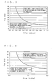
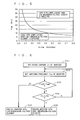
- Figs. 2 to 5 are graphs showing an area where it is desirable to employ a high-breakdown-voltage element based on Equations (9) and (10).
- Figs. 2 and 3 concern the third generation, and Figs. 4 and 5 concern the fifth generation.
- Selected for Fig. 2 is an IGBT element Q1 having turn-on losses EL and a saturation voltage VL of 1.30 (mJ/pulse) and 2.20 (V), respectively, and a breakdown voltage of 600 V.
- Selected for Fig. 3 is an IGBT element Q2 having turn-on losses EL and a saturation voltage VL of 1.04 (mJ/pulse) and 2.34 (V), respectively, and a breakdown voltage of 600 V.
- Selected for Fig. 1 is an IGBT element Q1 having turn-on losses EL and a saturation voltage VL of 1.30 (mJ/pulse) and 2.20 (V), respectively, and a breakdown voltage of 600 V.
- Selected for Fig. 3 is an
- FIG. 4 is an IGBT element Q3 having turn-on losses EL and a saturation voltage VL of 1.00 (mJ/pulse) and 1.1 (V), respectively, and a breakdown voltage of 600 V.
- Selected for Fig. 5 is an IGBT element Q4 having turn-on losses EL and a saturation voltage VL of 0.54 (mJ/pulse) and 1.40 (V), respectively, and a breakdown voltage of 600 V.
- the switching frequency fsw of the inverter increases, it is desirable to select a high-breakdown-voltage element in a range with a small increment ⁇ Esw of turn-on losses. Or to put it further, as the switching frequency fsw increases, it is desirable to select a high-breakdown-voltage element in a range with low turn-on losses Esw(on) in rated current. It is still further desirable that the increment ⁇ Esw of turn-on losses be negative (namely, the turn-on losses Esw(on) in the high-breakdown-voltage element be lower than the turn-on losses EL in the low-breakdown-voltage element).
- the losses can be reduced substantially lower than when the low-breakdown-voltage element is used regardless of the turn-on losses in the high-breakdown-voltage element. The reason for this is as follows.
- a third-generation 1200 V IGBT element Z1 has turn-on losses Esw(on) of 2.10 mJ/pulse, and a difference from the turn-on losses in a 600V IGBT element Q1 of the same generation is almost 0.8 mJ/pulse.
- a difference in turn-on losses between the IGBT element Z1 and a 600 V IGBT element Q2 of the same generation is almost 1.06 mJ/pulse.
- Fig. 2 concerning the IGBT element Q1 shows that the losses are smaller in the IGBT element having a breakdown voltage of 1200 V when an increment DEsw of turn-on losses is 0.8 mJ/pulse or less and the switching frequency fsw is 7 kHz.
- Fig. 3 concerning the IGBT element Q2 shows that the losses are smaller in the IGBT element having a breakdown voltage of 1200 V when an increment ⁇ Esw of turn-on losses is 1.10 mJ/pulse or less and the switching frequency fsw is 7 kHz.
- a fifth-generation 1200 V IGBT element Z2 has turn-on losses Esw(on) of 1.10 mJ/pulse, and a difference from the turn-on losses in a 600 V IGBT element Q3 of the same generation is almost 0.1 mJ/pulse.
- a difference in turn-on losses between the IGBT element Z2 and a 600 V IGBT element Q4 of the same generation is almost 0.56 mJ/pulse.
- Fig. 4 concerning the IGBT element Q3 shows that the losses are smaller in the IGBT element having a breakdown voltage of 1200 V when an increment ⁇ Esw of turn-on losses is almost 0.2 mJ/pulse or less and the switching frequency fsw is 7 kHz.
- Fig. 5 concerning the IGBT element Q4 shows that the losses are smaller in the IGBT element having a breakdown voltage of 1200 V when an increment ⁇ Esw of turn-on losses is 0.80 mJ/pulse or less and the switching frequency fsw is 7 kHz.
- a motor used for compressing a refrigerant is typically not required of a quick response to changes in the number of rotations and torque, and causes no noticeable noise since a refrigerant compressor including the motor is often covered to be used.
- a low switching frequency fsw capable of realizing an inverter at low cost is employed. For instance, a switching frequency of almost 10 kHz or more is selected for a motor for a use that requires noise control. Meanwhile, a switching frequency is set to about 3 kHz for an outdoor air conditioner unit that is installed outside and soundproof, and for a refrigerator having a compressor supported by a coil. In such ways, the employment of a high-breakdown-voltage element is especially effective for an inverter that supplies current to a motor employed for a refrigerant compressor.
- a preferred embodiment of the present invention will be described below, taking as an example an inverter that supplies current to a motor of a compressor of an air conditioner.
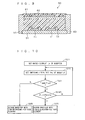
- Fig. 6 is a flowchart illustrating a method of designing a current supply circuit according to the present invention.
- a rated power G of the motor is predetermined based on the ability required of the compressor.
- an effective value voltage F of an AC power supply that is employed for driving the air conditioner including the motor and the inverter that supplies current to the motor.
- step S22 to set a switching frequency fsw based on the followability and so on of motor control by the inverter. As described later, the switching frequency fsw is reduced each time this step is performed.
- Step S23 is then performed to determine whether the switching frequency fsw is a predetermined minimum value fswo or more.
- the minimum value fswo is selected so that the above followability falls within a desirable range.
- step S24 is subsequently performed to determine whether losses PH in a high-breakdown-voltage element are lower than losses PL in a low-breakdown-voltage element. Although specifics are omitted at step S24, the respective magnitudes of the losses PL and PH are determined by combining various low-breakdown-voltage elements and various high-breakdown-voltage elements.
- step S24 processing then continues with step S25, to design the inverter with high-breakdown-voltage elements.
- step S24 When a negative determination is made at step S24, processing returns to step S22.
- the switching frequency fsw the likelier it becomes to design the inverter using high-breakdown-voltage elements (see Figs. 2 and 3, for example).
- the switching frequency fsw to be set is reduced each time step S22 is performed. After that, a determination is made again at step S23.
- step S23 processing then continues with step S26, to design the inverter with low-breakdown-voltage elements.
- IGBT elements to be employed for the inverter are selected appropriately based on the rated power G of the motor and the effective value voltage F of the AC power supply, which allows the losses in the inverter to be reduced.
- Current that may be passed from a high-breakdown-voltage element to be employed when designing the inverter with a high-breakdown-voltage element is smaller than current that may be passed from a high-breakdown-voltage element to be employed when designing the inverter with a low-breakdown-voltage element.
- current that may be passed from the high-breakdown-voltage element is half the current that may be sent from the low-breakdown-voltage element. This requires a smaller chip area of the IGBT element, offering the advantage of cost reduction.
- the rated voltage of a motor when designing the inverter with high-breakdown-voltage elements is k-fold the rated voltage of a motor when designing the inverter with low-breakdown-voltage elements (step S26), which is twice in the above example (when the high-breakdown-voltage element has a breakdown voltage of 1200 V, and the low-breakdown-voltage element has a breakdown voltage of 600 V).
- Fig. 7 is a circuit diagram illustrating a current-supplying technique with an inverter as designed above.
- the inverter 42 includes series connection of two IGBT elements having a breakdown voltage of 1200 V for each phase, and outputs an AC current of each phase from a node of the series connection to a three-phase motor M2.
- the smoothing circuit 32 includes no reactor.
- Fig. 8 is a circuit diagram illustrating the configuration of a three-phase voltage doubler circuit.
- the single-phase AC power supply 1 and is replaced with a three-phase AC power supply 13
- the diode bridge 22 is replaced with a diode bridge 23.
- the diode bridge 23 includes three capacitors for performing voltage doubler rectification. Again in this case, a DC voltage subjected to voltage doubler rectification is supplied to the inverter 42 via the smoothing circuit 32. Therefore, the aforementioned effects can be obtained by applying the present invention to form the inverter 42 with high-breakdown-voltage elements.
- the losses can be reduced further by the diode bridge 22 performing voltage doubler rectification than the diode bridge 21 performing full-wave rectification. This is because current passed from the AC power supply 1 always flows through two diodes in the diode bridge 21, whereas the diode bridge 22 includes capacitors for performing voltage doubler rectification and therefore includes only one diode in a current path from the AC power supply 1. Accordingly, looking at losses produced in a diode, the diode bridge 22 produces losses only half as much as the losses in the diode bridge 21.
- the power losses are calculated to be 2Pd.
- the diode bridge 22 performing voltage doubler rectification where there is only one diode in a current path from the AC power supply 1, the power losses are calculated to be Pd.
- a low-breakdown-voltage element or a high-breakdown-voltage element as an IGBT element in consideration of the losses in the diode bridge depends on, using the losses PL and PH in Equations (7) and (8), which one of PL + 2Pd and PH + Pd is higher. Put another way, a high-breakdown-voltage element should be selected when Equation (13) holds true and a low-breakdown-voltage element should be selected when Equation (13) does not hold true, to reduce the sum of the respective losses in the diode bridge and in the inverter. [ Numeral 13 ] PL > PH ⁇ P d
- Fig. 10 is a flowchart clarifying the above decision, which corresponds to Fig. 6.
- the step S24 in the Fig. 6 flowchart is replaced with step S24D to make a decision based on Equation (13).
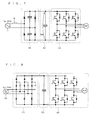
- Fig. 11 is a graph showing an area where it is desirable to employ a high-breakdown-voltage element in view of the sum of the respective losses in the diode bridge and in the inverter. Selected here is an IGBT element having turn-on losses EL and a saturation voltage VL of 1.04 (mJ/pulse) and 2.34 (V), respectively, and a breakdown voltage of 600 V, like the one described in regard to Fig. 3. Calculations were done by assuming that a forward voltage drop Vf is 1.5 V.
- the losses in the diode bridge and inverter can be reduced further when a high-breakdown-voltage element is employed than when a low-breakdown-voltage element is employed.
- the graph shown in Fig. 3 reappears as a curve 101.
- the curve 101 is nearer the origin side than the curve 102 is. Namely, in consideration of the losses in the diode bridge, an area capable of reducing the losses expands further when a high-breakdown-voltage element is employed than when a low-breakdown-voltage element is employed.
- Equation (9) is modified to Equation (14).
- Equation (9) f s w ⁇ [ P d + 1 8 ( VL ⁇ ⁇ V c e ) ⁇ I c p ] / [ ( 2 ⁇ ) ⁇ ⁇ E s w ]
- IGBT element has been used as a switching element of an inverter in the above description, the present invention is applicable in the same fashion with the use of other switching elements.
- the voltage obtained from the AC power supply 1 is not limited to have an effective value of 200 V.
- the present invention is applicable to a power supply having an effective value of 200 V to 240 V (referred to as a 200 V system power supply in the present invention), for example.
- Fig. 9 is a cross-sectional view illustrating a module structure disclosed in the patent document 2.
- Electric components within an electric motor controlling module 50 are mounted on a print substrate 62 and an aluminum substrate 61 that are vertically disposed almost in parallel with each other.
- the lines of the print substrate 62 and aluminum substrate 61 are connected via a resin-molded circuit plate 63.
- Power components 71 (which handle a little over ten watts of power) such as a diode and a power transistor in the electric motor controlling module 50 are all bare chip mounted on the aluminum substrate 61.
- an intra-module CPU formed of a one chip microcomputer including a microprocessor, a ROM, and various kinds of interfaces should be cut off from heat generation and noise by other electric components, and is therefore mounted on the print substrate 62 on which components with a great amount of heat generation are not mounted. Control components with no (or a little amount of) heat generation are also mounted on the print substrate 62.
- a molding material 81 covers the power components 71, a bonding wire 73, and the other components on the aluminum substrate 61. The molding material 81 covers the components on the print substrate 62 as well. Modularizing a diode bridge and an inverter is especially effective in a high-breakdown-voltage element, as discussed above.
Landscapes
- Engineering & Computer Science (AREA)
- Power Engineering (AREA)
- Inverter Devices (AREA)
Applications Claiming Priority (2)
| Application Number | Priority Date | Filing Date | Title |
|---|---|---|---|
| JP2003418283 | 2003-12-16 | ||
| PCT/JP2004/018732 WO2005060082A1 (ja) | 2003-12-16 | 2004-12-15 | 電流供給回路、多相駆動回路、電流供給回路設計方法 |
Publications (2)
| Publication Number | Publication Date |
|---|---|
| EP1701435A1 true EP1701435A1 (de) | 2006-09-13 |
| EP1701435A4 EP1701435A4 (de) | 2010-04-21 |
Family
ID=34697095
Family Applications (1)
| Application Number | Title | Priority Date | Filing Date |
|---|---|---|---|
| EP04807091A Withdrawn EP1701435A4 (de) | 2003-12-16 | 2004-12-15 | Stromquellenschaltung, mehrphasen-ansteuerschaltung, stromquellen-schaltungsentwurfverfahren |
Country Status (6)
| Country | Link |
|---|---|
| US (1) | US8743568B2 (de) |
| EP (1) | EP1701435A4 (de) |
| KR (1) | KR100832965B1 (de) |
| CN (1) | CN100495891C (de) |
| AU (1) | AU2004300366B2 (de) |
| WO (1) | WO2005060082A1 (de) |
Cited By (1)
| Publication number | Priority date | Publication date | Assignee | Title |
|---|---|---|---|---|
| US9178410B2 (en) | 2012-01-06 | 2015-11-03 | General Electric Company | Adaptive power conversion system |
Families Citing this family (2)
| Publication number | Priority date | Publication date | Assignee | Title |
|---|---|---|---|---|
| US7535737B2 (en) * | 2002-07-30 | 2009-05-19 | Daikin Industries, Ltd. | AC/AC multiple-phase power converter configured to be mounted on a substrate |
| US9252743B2 (en) * | 2012-09-28 | 2016-02-02 | Intel Corporation | Distributed polyphase filter |
Family Cites Families (9)
| Publication number | Priority date | Publication date | Assignee | Title |
|---|---|---|---|---|
| JPS60249895A (ja) | 1984-05-25 | 1985-12-10 | Toshiba Corp | 周波数変換装置 |
| JP3011482B2 (ja) * | 1991-06-04 | 2000-02-21 | 三洋電機株式会社 | 電子レンジ用電源装置 |
| JP3405878B2 (ja) | 1995-12-27 | 2003-05-12 | オリジン電気株式会社 | X線電源装置 |
| JP3419222B2 (ja) | 1996-11-15 | 2003-06-23 | 松下電器産業株式会社 | 空調用インバータ装置 |
| JPH11136994A (ja) * | 1997-10-31 | 1999-05-21 | Hitachi Ltd | 3相誘導電動機駆動装置 |
| JP3777805B2 (ja) * | 1998-07-13 | 2006-05-24 | 松下電器産業株式会社 | インバータ装置 |
| JP2002165464A (ja) * | 2000-10-24 | 2002-06-07 | Samsung Electronics Co Ltd | インバータ印刷回路基板 |
| JP3641581B2 (ja) * | 2000-10-24 | 2005-04-20 | 株式会社東芝 | ドラム式洗濯機 |
| JP2003143871A (ja) | 2001-11-01 | 2003-05-16 | Daikin Ind Ltd | 電動機制御モジュールおよびそれを備えた空気調和装置 |
-
2004
- 2004-12-15 EP EP04807091A patent/EP1701435A4/de not_active Withdrawn
- 2004-12-15 AU AU2004300366A patent/AU2004300366B2/en not_active Revoked
- 2004-12-15 KR KR1020067011719A patent/KR100832965B1/ko not_active Expired - Fee Related
- 2004-12-15 WO PCT/JP2004/018732 patent/WO2005060082A1/ja not_active Ceased
- 2004-12-15 CN CNB2004800371580A patent/CN100495891C/zh not_active Expired - Fee Related
- 2004-12-15 US US10/582,936 patent/US8743568B2/en not_active Expired - Fee Related
Cited By (1)
| Publication number | Priority date | Publication date | Assignee | Title |
|---|---|---|---|---|
| US9178410B2 (en) | 2012-01-06 | 2015-11-03 | General Electric Company | Adaptive power conversion system |
Also Published As
| Publication number | Publication date |
|---|---|
| AU2004300366A1 (en) | 2005-06-30 |
| US20070139978A1 (en) | 2007-06-21 |
| CN100495891C (zh) | 2009-06-03 |
| EP1701435A4 (de) | 2010-04-21 |
| CN1894846A (zh) | 2007-01-10 |
| KR20060100468A (ko) | 2006-09-20 |
| US8743568B2 (en) | 2014-06-03 |
| AU2004300366B2 (en) | 2007-11-22 |
| WO2005060082A1 (ja) | 2005-06-30 |
| KR100832965B1 (ko) | 2008-06-05 |
Similar Documents
| Publication | Publication Date | Title |
|---|---|---|
| Teichmann et al. | A comparison of three-level converters versus two-level converters for low-voltage drives, traction, and utility applications | |
| US9941834B2 (en) | Power conversion apparatus and air-conditioning apparatus including the power conversion apparatus | |
| US20150365040A1 (en) | Rotary Electric Machine Driving Device | |
| US20020131285A1 (en) | Control device for power converter | |
| US20150365038A1 (en) | Rotary Electric Machine Driving Device | |
| JP2007104778A (ja) | 車載用電動機制御装置 | |
| US20210313902A1 (en) | Direct-current power supply apparatus, motor drive control apparatus, blower, compressor, and air conditioner | |
| JP6423323B2 (ja) | 電力変換装置 | |
| US8743568B2 (en) | Current supply circuit, polyphase drive circuit, method of designing current supply circuit | |
| US20150357960A1 (en) | Rotary electric machine driving device | |
| Barrera-Cardenas et al. | A Meta-Parameterized Approach for the Evaluation of Semiconductor Technologies—A Comparison between SiC-MOSFET and Si-IGBT Technologies— | |
| KR20180087601A (ko) | 노이즈 저감 기능을 가지는 전력 변환 장치 및 이를 포함하는 공기 조화기 | |
| AU2008200796B2 (en) | Current supply circuit, polyphase drive circuit, method of designing current supply circuit | |
| US20230246561A1 (en) | Power converter and heat pump system provided therewith | |
| JP3687678B2 (ja) | 電流供給回路設計方法及び電流供給回路並びに多相駆動回路 | |
| JP6710281B2 (ja) | 電力変換装置 | |
| JP4517762B2 (ja) | スイッチング制御方法、整流装置及び駆動システム | |
| Brinker et al. | Design of a hybrid two-stage GaN-Si inverter for BLDC motors | |
| Mueller et al. | New HybridPACKTM HD–Key to Reliable Highest Performance eTRUCK Inverters for Heavy-Duty Operation | |
| KR102069067B1 (ko) | 리플 저감 정류부를 포함하는 전력 변환 장치 및 이를 포함하는 공기 조화기 | |
| KR102007852B1 (ko) | 전력 변환 장치 및 이를 포함하는 공기 조화기 | |
| RU2817330C1 (ru) | Преобразователь мощности и система теплового насоса, снабженная им | |
| KR20180137994A (ko) | 전력 변환 장치 및 그 제어 방법 | |
| Abbatelli et al. | SiC and Silicon MOSFET solution for high frequency DC-AC converters | |
| US20250226769A1 (en) | Power conversion device and refrigeration cycle applied equipment |
Legal Events
| Date | Code | Title | Description |
|---|---|---|---|
| PUAI | Public reference made under article 153(3) epc to a published international application that has entered the european phase |
Free format text: ORIGINAL CODE: 0009012 |
|
| 17P | Request for examination filed |
Effective date: 20060706 |
|
| AK | Designated contracting states |
Kind code of ref document: A1 Designated state(s): AT BE BG CH CY CZ DE DK EE ES FI FR GB GR HU IE IS IT LI LT LU MC NL PL PT RO SE SI SK TR |
|
| DAX | Request for extension of the european patent (deleted) | ||
| A4 | Supplementary search report drawn up and despatched |
Effective date: 20100322 |
|
| 17Q | First examination report despatched |
Effective date: 20100611 |
|
| STAA | Information on the status of an ep patent application or granted ep patent |
Free format text: STATUS: THE APPLICATION HAS BEEN WITHDRAWN |
|
| 18W | Application withdrawn |
Effective date: 20160926 |