EP1701531A1 - Unterspannungsunterdrückungsschaltung - Google Patents
Unterspannungsunterdrückungsschaltung Download PDFInfo
- Publication number
- EP1701531A1 EP1701531A1 EP05300170A EP05300170A EP1701531A1 EP 1701531 A1 EP1701531 A1 EP 1701531A1 EP 05300170 A EP05300170 A EP 05300170A EP 05300170 A EP05300170 A EP 05300170A EP 1701531 A1 EP1701531 A1 EP 1701531A1
- Authority
- EP
- European Patent Office
- Prior art keywords
- power source
- source
- voltage
- switch
- capacitors
- Prior art date
- Legal status (The legal status is an assumption and is not a legal conclusion. Google has not performed a legal analysis and makes no representation as to the accuracy of the status listed.)
- Granted
Links
Images


Classifications
-
- H—ELECTRICITY
- H04—ELECTRIC COMMUNICATION TECHNIQUE
- H04M—TELEPHONIC COMMUNICATION
- H04M19/00—Current supply arrangements for telephone systems
- H04M19/001—Current supply source at the exchanger providing current to substations
- H04M19/008—Using DC/DC converters
-
- H—ELECTRICITY
- H02—GENERATION; CONVERSION OR DISTRIBUTION OF ELECTRIC POWER
- H02J—ELECTRIC POWER NETWORKS; CIRCUIT ARRANGEMENTS OR SYSTEMS FOR SUPPLYING OR DISTRIBUTING ELECTRIC POWER; SYSTEMS FOR STORING ELECTRIC ENERGY
- H02J9/00—Circuit arrangements for emergency or stand-by power supply, e.g. for emergency lighting
- H02J9/04—Circuit arrangements for emergency or stand-by power supply, e.g. for emergency lighting in which the distribution system is disconnected from the normal source and connected to a standby source
- H02J9/06—Circuit arrangements for emergency or stand-by power supply, e.g. for emergency lighting in which the distribution system is disconnected from the normal source and connected to a standby source with automatic change-over, e.g. UPS systems
- H02J9/062—Circuit arrangements for emergency or stand-by power supply, e.g. for emergency lighting in which the distribution system is disconnected from the normal source and connected to a standby source with automatic change-over, e.g. UPS systems for AC powered loads
-
- H—ELECTRICITY
- H02—GENERATION; CONVERSION OR DISTRIBUTION OF ELECTRIC POWER
- H02J—ELECTRIC POWER NETWORKS; CIRCUIT ARRANGEMENTS OR SYSTEMS FOR SUPPLYING OR DISTRIBUTING ELECTRIC POWER; SYSTEMS FOR STORING ELECTRIC ENERGY
- H02J7/00—Circuit arrangements for charging or discharging batteries or for supplying loads from batteries
- H02J7/34—Parallel operation in networks using both storage and other DC sources, e.g. providing buffering
- H02J7/345—Parallel operation in networks using both storage and other DC sources, e.g. providing buffering using capacitors as storage or buffering devices
Definitions
- the invention relates to a protection device enabling a load to withstand a transient power supply failure.
- a protection device can be used in particular in a switching equipment for telecommunications, which requires a supply voltage always greater than a minimum value set.
- Such telecommunication equipment consists of electronic cards inserted into the connectors of a backplane, the backplane providing power to a plurality of cards, with a DC voltage of 48V generally.
- All these cards are connected in parallel for their feeding. If a short circuit occurs on a card, and if it short-circuits the card's power input, it fuses a card-specific fuse. By fusing the fuse, this card is disconnected from the power source after a delay of the order of a few milliseconds. During this time, the voltage of the power source can be practically zero because of the short-circuit.
- the cards are all powered in parallel, they can not work properly during this time, if they are not protected against such a transient power failure.
- These cards generally include several filter capacitors connected in parallel to the power input of the card, and a DC-DC converter, converting the voltage of 48V into one or more lower DC voltages, 5V and 3.3V, for example .
- This converter can only work properly in a well-defined input voltage range, for example 36V to 72V.
- each card is connected to the power source (or power sources) by a switching system generally consisting of diodes, so that these filtering capacitors can charge when the source of Power supply operates normally, and can not discharge when the power source is short-circuited.
- a switching system generally consisting of diodes, so that these filtering capacitors can charge when the source of Power supply operates normally, and can not discharge when the power source is short-circuited.
- the power source generally consists of two sources connected in parallel by diodes,
- the filter capacitors placed in parallel on the power input of each card have a very high total capacitance, for example 10,000 microfarads for a 200W consuming card.
- the volume occupied by these capacitors is then very important and these capacitors significantly increase the capacitance. cost of the card.
- the object of the invention is to propose another less bulky and less expensive solution to allow a load to withstand a transient power failure.
- the device thus characterized protects the load against a drop in voltage because the series connection of the two storage capacitors momentarily creates a voltage source whose initial voltage is theoretically equal to the sum of the charging voltages of these two capacitors.
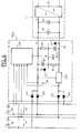
- the load L is for example an electronic card comprising a series of filter capacitors C1, ..., Cn and a DC / DC converter CV all connected in parallel to the two inputs of the load L.
- the slow start circuit SSC is a conventional electronic circuit whose function is to limit the overcurrent caused by the charge of the capacitors located downstream, in particular SC1, SC2, C1,..., Cn, during the insertion of the board in a backplane, or when powering up the backplane.
- Figure 1 shows the state where these switches are when each power source B1, 82 has normal operation.
- the control unit CU1 detects that Ve has a value (approximately 47V) less than V1 and V2 (approximately 48V), that is to say that the diodes D1 to D4 are on. It controls the switches SW1 and SW2 to be closed and SW3 to be open, so that the capacitors SC1 and SC2 are both connected in parallel to the outputs of the device PD1.
- the capacitors SC1 and SC2 are charged to the voltage supplied by the sources B1 and B2, through the diodes D1,..., D4, ie approximately 47V. During this normal operation, they add a certain filtering effect to that of the capacitors C1, ..., Cn.
- FIG. 2 represents the diagram of this same exemplary embodiment, showing the state of the switches SW1, SW2, SW3 when each power source B1, B2 has a transient failure due to a short-circuit on one of the loads other than L.
- the protection device PD1 the voltages V1 and V2 suddenly becoming lower than the voltage Ve, the diodes D1, D2, D3, D4 are blocked and isolate the device PD1 from the sources B1 and B2 which are short-circuited. They prevent the short circuit from discharging the capacitors SC1 and SC2.
- the voltage across the capacitors SC1, SC2, C1, ..., Cn begins to decrease gradually because they discharge by supplying the CV converter.
- the control unit CU1 concludes that there is a failure of sources B1 and B2; and it then controls the switches SW1 and SW2 to be open. After a delay necessary for this opening (10 microseconds for example), it controls the closing of the switch SW3 so that the capacitors SC1 and SC2 are connected in series.
- This set is then in parallel on the outputs of the device PD1, and theoretically provides (if there were no filter capacitors C1, ..., Cn) a voltage equal to the sum of the capacitor charge voltage C1 and the charging voltage of the capacitor C2, at the time of switching, about 94V.
- This voltage is recited by the attenuation capacitors C1, ..., Cn.
- the contribution of charge to these capacitors C1, ..., Cn provides an initial voltage of 82V in an exemplary embodiment.
- This voltage then decreases, but it makes it possible to supply the load L with a voltage greater than 36 V for a delay at least equal to 5 ms (delay fixed by the ATCA standard, Advanced Telecommunications Computing Architecture), 36 V being the minimum value required. to the correct operation of the CV converter in this example.
- the time constants are chosen such that the three transistors that make up the switches SW1, SW2, SW3 can not be conductors simultaneously.
- the control unit CU1 detects that the voltage Ve has a value (approximately 47V) which has returned to greater than V1 and V2, for a duration greater than a fixed threshold (5 ms for example). It first controls switch SW3 to open. After a delay necessary for this opening (100 microseconds for example), it controls the switches SW1 and SW2 so that they are closed, so that the capacitors SC1 and SC2 are connected both in parallel on the outputs of the device PD1. They are recharged to the voltage provided by the sources B1 and B2, through the diodes D1, ..., D4, or about 47V.
- a fixed threshold 5 ms for example
- FIG. 3 represents the block diagram of a variant PD1 'of this first exemplary embodiment.
- the control unit CU1 is replaced by a control unit CU1 'which has only one pair of inputs, one input being connected to the cathodes of the diodes D1 and D3 on the one hand, and another input being connected at the anodes of diodes D2 and D4 on the other hand.
- the control unit CU1 controls the switches SW1 and SW3 to be open. After a delay necessary for this opening (10 microseconds for example), it commands the closing of the SW2 switch, so that capacitors SC1 and SC2 are connected in series.
- This set is then in parallel on the outputs of the device PD1, and provides a voltage equal to the sum of the charging voltage of the capacitor C1 and the charging voltage of the capacitor C2, at the moment of switching, that is approximately 82V initially.
- the control unit CU1 When the short circuit is completed, the control unit CU1 'detects that the voltage Ve has a thief (approximately 47V) which has returned to greater than the threshold value (41V) for a duration greater than a fixed threshold (for example 5ms). ). It first controls switch SW3 to open. After a delay necessary for this opening (100 microseconds for example), it controls the switches SW1 and SW2 so that they are closed, so that the capacitors SC1 and SC2 are connected both in parallel on the outputs of the device PD1. They are recharged to the voltage provided by the sources B1 and B2, through the diodes D1, ..., D4, or about 47V.
- FIG. 4 represents the block diagram of a second exemplary embodiment PD2 of the protection device according to the invention, the realization of which is simpler since it comprises only one electronic switch SW3. It differs from the first example in that the electronic switches SW1 and SW2 are replaced respectively by resistors R1 and R2.
- the control unit CU2 is similar to the control unit CU1 of the first exemplary embodiment PD1, for example, but has a single output which controls the switch SW3.
- FIG. 4 represents the state where the switch SW3 is when each power source B1, B2 has normal operation.
- the control unit CU2 detects that the voltage Ve has a value (approximately 47V) less than V1 and V2 (FIG. Approximately 48V), that is to say that the diodes D1 to D4 are busy. It controls the switch SW3 so that it is open, so that the capacitors SC1 and SC2 are connected both in parallel to the outputs of the device PD1, respectively by the resistors R1 and R2.
- the capacitors SC1 and SC2 are charged to the voltage supplied by the sources B1 and B2, through the diodes D1,..., D4, ie approximately 47V.
- FIG. 5 represents the block diagram of this second exemplary embodiment PD2, in the state where it is when the power source B1, B2 has a transient failure due to a short circuit on one of the loads other than L.
- the protection device PD2 the voltages V1 and V2 suddenly becoming lower than the voltage Ve, the diodes D1, D2, D3, D4 are blocked and isolate the PD2 device sources B1 and B2 which are short-circuited. They prevent the short circuit from discharging the capacitors SC1 and SC2.
- the voltage across the capacitors SC1, SC2, C1, .., Cn begins to decrease gradually because they discharge by supplying the CV converter.
- the control unit CU2 concludes that there is a failure of the sources B1 and 82; and then it controls the switch SW3 to be closed.
- the capacitors SC1 and SC2 are then connected in series.
- the resistor R1 is in parallel with the capacitor SC2.
- Resistor R2 is in parallel with capacitor SC1.
- the time constants R2 x SC1 and R1 x SC2 are chosen much longer than 5 ms for the discharge caused by these resistors to be negligible,
- the set of two capacitors, SC1-SC2 connected in series, is then in parallel on the outputs of the device PD1, and provides a voltage equal to the sum of the charging voltage of the capacitor C1 and the charging voltage of the capacitor C2 at the time of switching, approximately 82V initially.
- the control unit CU2 detects that the voltage Ve has a value (approximately 47V) which has returned to greater than V1 and V2 for a duration greater than a fixed threshold (for example 5ms). switch SW3 to open.
- the capacitors SC1 and SC2 are again connected both in parallel to the outputs of the device PD2. They are recharged to the voltage provided by the sources B1 and B2, through the diodes D1, ..., D4, or about 47V.
- control unit CU1 'described with reference to FIG. 3 could also be used to control the switch SW3 of this second exemplary embodiment, in place of the unit CU2.
- FIG. 6 represents the block diagram of a variant PD3 of this second exemplary embodiment, making it possible to use storage capacitors SC1 and SC2, designed for a lower operating voltage, which significantly reduces their cost and size.
- a Zener diode Z1 is connected in parallel with the capacitor C1 and a Zener diode Z2 is connected in parallel with the capacitor C2.
- the Zener diode Z1 cooperates with the resistor R1 to charge the capacitor C1 by limiting the charging voltage to 47 V.
- the Zener diode Z2 collaborates with the resistor R2 to charge the capacitor C2 by limiting the charging voltage to 47V.
Landscapes
- Engineering & Computer Science (AREA)
- Signal Processing (AREA)
- Business, Economics & Management (AREA)
- Emergency Management (AREA)
- Power Engineering (AREA)
- Direct Current Feeding And Distribution (AREA)
- Charge And Discharge Circuits For Batteries Or The Like (AREA)
- Logic Circuits (AREA)
- Amplifiers (AREA)
- Dc-Dc Converters (AREA)
- Stand-By Power Supply Arrangements (AREA)
Priority Applications (5)
| Application Number | Priority Date | Filing Date | Title |
|---|---|---|---|
| EP05300170A EP1701531B1 (de) | 2005-03-08 | 2005-03-08 | Unterspannungsunterdrückungsschaltung |
| AT05300170T ATE394010T1 (de) | 2005-03-08 | 2005-03-08 | Unterspannungsunterdrückungsschaltung |
| DE602005006380T DE602005006380T2 (de) | 2005-03-08 | 2005-03-08 | Unterspannungsunterdrückungsschaltung |
| US11/368,396 US20060203413A1 (en) | 2005-03-08 | 2006-03-07 | Protection circuit enabling a load to withstand a transient power supply failure |
| CNB2006100586812A CN100479305C (zh) | 2005-03-08 | 2006-03-08 | 使负载能够抵御瞬时电源故障的保护电路 |
Applications Claiming Priority (1)
| Application Number | Priority Date | Filing Date | Title |
|---|---|---|---|
| EP05300170A EP1701531B1 (de) | 2005-03-08 | 2005-03-08 | Unterspannungsunterdrückungsschaltung |
Publications (2)
| Publication Number | Publication Date |
|---|---|
| EP1701531A1 true EP1701531A1 (de) | 2006-09-13 |
| EP1701531B1 EP1701531B1 (de) | 2008-04-30 |
Family
ID=34942511
Family Applications (1)
| Application Number | Title | Priority Date | Filing Date |
|---|---|---|---|
| EP05300170A Not-in-force EP1701531B1 (de) | 2005-03-08 | 2005-03-08 | Unterspannungsunterdrückungsschaltung |
Country Status (5)
| Country | Link |
|---|---|
| US (1) | US20060203413A1 (de) |
| EP (1) | EP1701531B1 (de) |
| CN (1) | CN100479305C (de) |
| AT (1) | ATE394010T1 (de) |
| DE (1) | DE602005006380T2 (de) |
Cited By (1)
| Publication number | Priority date | Publication date | Assignee | Title |
|---|---|---|---|---|
| EP3098952A3 (de) * | 2015-05-05 | 2017-03-15 | Control Techniques Ltd | Laufwerk niedriger kapazität mit verbesserter immunität |
Families Citing this family (2)
| Publication number | Priority date | Publication date | Assignee | Title |
|---|---|---|---|---|
| US7605572B2 (en) * | 2005-03-31 | 2009-10-20 | Virginia Tech Intellectual Properties, Inc. | Input current sensing AVP method for future VRM |
| KR20150074395A (ko) * | 2013-12-24 | 2015-07-02 | 현대자동차주식회사 | 파워 팩터 코렉터의 출력 커패시터의 정전용량 값 변경 방법 및 변경 회로 |
Citations (4)
| Publication number | Priority date | Publication date | Assignee | Title |
|---|---|---|---|---|
| EP0626744A1 (de) * | 1993-05-27 | 1994-11-30 | Alcatel Cit | Strombegrenzungsvorrichtung zwischen einer Leiterplatte und einer Stromversorgung |
| US5945816A (en) * | 1998-04-21 | 1999-08-31 | Alcatel Network Systems, Inc. | Self-biased power isolator system |
| US5973547A (en) * | 1997-06-27 | 1999-10-26 | Sun Microsystems, Inc | Self-biasing, offset-nulling power supply monitor circuit |
| US20040135622A1 (en) * | 2003-01-14 | 2004-07-15 | Masleid Robert P. | Optimal inductor management |
Family Cites Families (2)
| Publication number | Priority date | Publication date | Assignee | Title |
|---|---|---|---|---|
| DE69318940T2 (de) * | 1992-11-12 | 1999-03-18 | Dhv International, Inc., Ventura, Calif. | Stromversorgungssystem für Bohrlochanlage |
| US6392387B1 (en) * | 2000-03-14 | 2002-05-21 | Sage Electronics And Technology, Inc. | Passively protected battery pack with on load charge and on load conditioning-discharge capability and charging system |
-
2005
- 2005-03-08 EP EP05300170A patent/EP1701531B1/de not_active Not-in-force
- 2005-03-08 AT AT05300170T patent/ATE394010T1/de not_active IP Right Cessation
- 2005-03-08 DE DE602005006380T patent/DE602005006380T2/de not_active Expired - Fee Related
-
2006
- 2006-03-07 US US11/368,396 patent/US20060203413A1/en not_active Abandoned
- 2006-03-08 CN CNB2006100586812A patent/CN100479305C/zh not_active Expired - Fee Related
Patent Citations (4)
| Publication number | Priority date | Publication date | Assignee | Title |
|---|---|---|---|---|
| EP0626744A1 (de) * | 1993-05-27 | 1994-11-30 | Alcatel Cit | Strombegrenzungsvorrichtung zwischen einer Leiterplatte und einer Stromversorgung |
| US5973547A (en) * | 1997-06-27 | 1999-10-26 | Sun Microsystems, Inc | Self-biasing, offset-nulling power supply monitor circuit |
| US5945816A (en) * | 1998-04-21 | 1999-08-31 | Alcatel Network Systems, Inc. | Self-biased power isolator system |
| US20040135622A1 (en) * | 2003-01-14 | 2004-07-15 | Masleid Robert P. | Optimal inductor management |
Cited By (1)
| Publication number | Priority date | Publication date | Assignee | Title |
|---|---|---|---|---|
| EP3098952A3 (de) * | 2015-05-05 | 2017-03-15 | Control Techniques Ltd | Laufwerk niedriger kapazität mit verbesserter immunität |
Also Published As
| Publication number | Publication date |
|---|---|
| DE602005006380D1 (de) | 2008-06-12 |
| DE602005006380T2 (de) | 2009-06-10 |
| CN100479305C (zh) | 2009-04-15 |
| ATE394010T1 (de) | 2008-05-15 |
| EP1701531B1 (de) | 2008-04-30 |
| US20060203413A1 (en) | 2006-09-14 |
| CN1835361A (zh) | 2006-09-20 |
Similar Documents
| Publication | Publication Date | Title |
|---|---|---|
| EP2085268B1 (de) | Elektronisches System für Batterie | |
| EP0110775B1 (de) | Regulierungseinrichtung mit kleiner Verlustspannung | |
| EP1446855B1 (de) | Elektrisches energiespeiseverfahren und -vorrichtung für ein gerät | |
| EP2351188B1 (de) | Ununterbrechbare gleichstrom-stromversorgungseinrichtung für ein datenverarbeitungssystem mit mindestens einem prozessor | |
| EP0847124B1 (de) | Notstromversorgungseinrichtung zur provisorischen Stromversorgung im Falle eines Versagens der Hauptstromversorgung | |
| FR2750507A1 (fr) | Procede de prediction de la capacite d'une batterie, unite de batterie, et appareil utilisant l'unite de batterie | |
| WO2011003924A1 (fr) | Batterie d'accumulateurs a pertes reduites | |
| EP4189406A1 (de) | Batterieverwaltungssystem | |
| EP3171482B1 (de) | Elektrische batterie, die ein elektronisches steuerungssystem umfasst | |
| EP2363939A2 (de) | Unterbrechungsfreie Wechselstromversorgung einer Installation und Verfahren dazu | |
| EP1701531B1 (de) | Unterspannungsunterdrückungsschaltung | |
| EP3883105A1 (de) | Vorrichtung zum entladen eines kondesators | |
| FR2908939A1 (fr) | Dispositif de commande pour assurer la regulation en tension d'un bus d'alimentation. | |
| CA2281637C (fr) | Dispositif d'alimentation faible cout d'une pluralite de modules electroniques installes dans une baie | |
| EP0626744B1 (de) | Strombegrenzungsvorrichtung zwischen einer Leiterplatte und einer Stromversorgung | |
| FR2810809A1 (fr) | Dispositif d'alimentation pour appareils electriques portables | |
| EP1177613A1 (de) | Telefonleitungsgespeistes stromversorgungssystem | |
| CA2605800A1 (fr) | Circuit d'alimentation sans interruption | |
| FR2474776A1 (fr) | Appareil pour la charge d'une batterie rechargeable | |
| FR2535930A1 (fr) | Ensemble portatif autonome pour le controle d'equipement d'eclairage public | |
| WO1991018339A1 (fr) | Dispositif de protection externe de systemes informatiques a l'egard des microcoupures de l'alimentation electrique | |
| FR2796502A1 (fr) | Installation de securite pour camera thermique | |
| FR2793355A1 (fr) | Dispositif de protection a commande d'ouverture de securite | |
| EP1177673A1 (de) | Telefonleitungsgespeistes stromversorgungssystem | |
| WO1991018340A1 (fr) | Dispositif de protection externe de systemes informatiques a l'egard des coupures de l'alimentation electrique |
Legal Events
| Date | Code | Title | Description |
|---|---|---|---|
| PUAI | Public reference made under article 153(3) epc to a published international application that has entered the european phase |
Free format text: ORIGINAL CODE: 0009012 |
|
| AK | Designated contracting states |
Kind code of ref document: A1 Designated state(s): AT BE BG CH CY CZ DE DK EE ES FI FR GB GR HU IE IS IT LI LT LU MC NL PL PT RO SE SI SK TR |
|
| AX | Request for extension of the european patent |
Extension state: AL BA HR LV MK YU |
|
| 17P | Request for examination filed |
Effective date: 20061229 |
|
| RAP1 | Party data changed (applicant data changed or rights of an application transferred) |
Owner name: ALCATEL LUCENT |
|
| AKX | Designation fees paid |
Designated state(s): AT BE BG CH CY CZ DE DK EE ES FI FR GB GR HU IE IS IT LI LT LU MC NL PL PT RO SE SI SK TR |
|
| GRAP | Despatch of communication of intention to grant a patent |
Free format text: ORIGINAL CODE: EPIDOSNIGR1 |
|
| GRAS | Grant fee paid |
Free format text: ORIGINAL CODE: EPIDOSNIGR3 |
|
| GRAA | (expected) grant |
Free format text: ORIGINAL CODE: 0009210 |
|
| AK | Designated contracting states |
Kind code of ref document: B1 Designated state(s): AT BE BG CH CY CZ DE DK EE ES FI FR GB GR HU IE IS IT LI LT LU MC NL PL PT RO SE SI SK TR |
|
| REG | Reference to a national code |
Ref country code: GB Ref legal event code: FG4D Free format text: NOT ENGLISH |
|
| REG | Reference to a national code |
Ref country code: CH Ref legal event code: EP |
|
| REG | Reference to a national code |
Ref country code: IE Ref legal event code: FG4D |
|
| REF | Corresponds to: |
Ref document number: 602005006380 Country of ref document: DE Date of ref document: 20080612 Kind code of ref document: P |
|
| PG25 | Lapsed in a contracting state [announced via postgrant information from national office to epo] |
Ref country code: SI Free format text: LAPSE BECAUSE OF FAILURE TO SUBMIT A TRANSLATION OF THE DESCRIPTION OR TO PAY THE FEE WITHIN THE PRESCRIBED TIME-LIMIT Effective date: 20080430 |
|
| NLV1 | Nl: lapsed or annulled due to failure to fulfill the requirements of art. 29p and 29m of the patents act | ||
| PG25 | Lapsed in a contracting state [announced via postgrant information from national office to epo] |
Ref country code: BG Free format text: LAPSE BECAUSE OF FAILURE TO SUBMIT A TRANSLATION OF THE DESCRIPTION OR TO PAY THE FEE WITHIN THE PRESCRIBED TIME-LIMIT Effective date: 20080730 Ref country code: FI Free format text: LAPSE BECAUSE OF FAILURE TO SUBMIT A TRANSLATION OF THE DESCRIPTION OR TO PAY THE FEE WITHIN THE PRESCRIBED TIME-LIMIT Effective date: 20080430 Ref country code: PT Free format text: LAPSE BECAUSE OF FAILURE TO SUBMIT A TRANSLATION OF THE DESCRIPTION OR TO PAY THE FEE WITHIN THE PRESCRIBED TIME-LIMIT Effective date: 20080930 Ref country code: NL Free format text: LAPSE BECAUSE OF FAILURE TO SUBMIT A TRANSLATION OF THE DESCRIPTION OR TO PAY THE FEE WITHIN THE PRESCRIBED TIME-LIMIT Effective date: 20080430 Ref country code: ES Free format text: LAPSE BECAUSE OF FAILURE TO SUBMIT A TRANSLATION OF THE DESCRIPTION OR TO PAY THE FEE WITHIN THE PRESCRIBED TIME-LIMIT Effective date: 20080810 |
|
| PG25 | Lapsed in a contracting state [announced via postgrant information from national office to epo] |
Ref country code: PL Free format text: LAPSE BECAUSE OF FAILURE TO SUBMIT A TRANSLATION OF THE DESCRIPTION OR TO PAY THE FEE WITHIN THE PRESCRIBED TIME-LIMIT Effective date: 20080430 Ref country code: AT Free format text: LAPSE BECAUSE OF FAILURE TO SUBMIT A TRANSLATION OF THE DESCRIPTION OR TO PAY THE FEE WITHIN THE PRESCRIBED TIME-LIMIT Effective date: 20080430 |
|
| REG | Reference to a national code |
Ref country code: IE Ref legal event code: FD4D |
|
| PG25 | Lapsed in a contracting state [announced via postgrant information from national office to epo] |
Ref country code: IS Free format text: LAPSE BECAUSE OF FAILURE TO SUBMIT A TRANSLATION OF THE DESCRIPTION OR TO PAY THE FEE WITHIN THE PRESCRIBED TIME-LIMIT Effective date: 20080830 |
|
| PG25 | Lapsed in a contracting state [announced via postgrant information from national office to epo] |
Ref country code: DK Free format text: LAPSE BECAUSE OF FAILURE TO SUBMIT A TRANSLATION OF THE DESCRIPTION OR TO PAY THE FEE WITHIN THE PRESCRIBED TIME-LIMIT Effective date: 20080430 Ref country code: SE Free format text: LAPSE BECAUSE OF FAILURE TO SUBMIT A TRANSLATION OF THE DESCRIPTION OR TO PAY THE FEE WITHIN THE PRESCRIBED TIME-LIMIT Effective date: 20080731 Ref country code: CZ Free format text: LAPSE BECAUSE OF FAILURE TO SUBMIT A TRANSLATION OF THE DESCRIPTION OR TO PAY THE FEE WITHIN THE PRESCRIBED TIME-LIMIT Effective date: 20080430 Ref country code: LT Free format text: LAPSE BECAUSE OF FAILURE TO SUBMIT A TRANSLATION OF THE DESCRIPTION OR TO PAY THE FEE WITHIN THE PRESCRIBED TIME-LIMIT Effective date: 20080430 Ref country code: IE Free format text: LAPSE BECAUSE OF FAILURE TO SUBMIT A TRANSLATION OF THE DESCRIPTION OR TO PAY THE FEE WITHIN THE PRESCRIBED TIME-LIMIT Effective date: 20080430 |
|
| PG25 | Lapsed in a contracting state [announced via postgrant information from national office to epo] |
Ref country code: RO Free format text: LAPSE BECAUSE OF FAILURE TO SUBMIT A TRANSLATION OF THE DESCRIPTION OR TO PAY THE FEE WITHIN THE PRESCRIBED TIME-LIMIT Effective date: 20080430 Ref country code: SK Free format text: LAPSE BECAUSE OF FAILURE TO SUBMIT A TRANSLATION OF THE DESCRIPTION OR TO PAY THE FEE WITHIN THE PRESCRIBED TIME-LIMIT Effective date: 20080430 |
|
| PLBE | No opposition filed within time limit |
Free format text: ORIGINAL CODE: 0009261 |
|
| STAA | Information on the status of an ep patent application or granted ep patent |
Free format text: STATUS: NO OPPOSITION FILED WITHIN TIME LIMIT |
|
| 26N | No opposition filed |
Effective date: 20090202 |
|
| PG25 | Lapsed in a contracting state [announced via postgrant information from national office to epo] |
Ref country code: EE Free format text: LAPSE BECAUSE OF FAILURE TO SUBMIT A TRANSLATION OF THE DESCRIPTION OR TO PAY THE FEE WITHIN THE PRESCRIBED TIME-LIMIT Effective date: 20080430 |
|
| PG25 | Lapsed in a contracting state [announced via postgrant information from national office to epo] |
Ref country code: IT Free format text: LAPSE BECAUSE OF FAILURE TO SUBMIT A TRANSLATION OF THE DESCRIPTION OR TO PAY THE FEE WITHIN THE PRESCRIBED TIME-LIMIT Effective date: 20080430 |
|
| BERE | Be: lapsed |
Owner name: ALCATEL LUCENT Effective date: 20090331 |
|
| PG25 | Lapsed in a contracting state [announced via postgrant information from national office to epo] |
Ref country code: MC Free format text: LAPSE BECAUSE OF NON-PAYMENT OF DUE FEES Effective date: 20090331 |
|
| PGFP | Annual fee paid to national office [announced via postgrant information from national office to epo] |
Ref country code: FR Payment date: 20090312 Year of fee payment: 5 |
|
| REG | Reference to a national code |
Ref country code: CH Ref legal event code: PL |
|
| GBPC | Gb: european patent ceased through non-payment of renewal fee |
Effective date: 20090308 |
|
| PG25 | Lapsed in a contracting state [announced via postgrant information from national office to epo] |
Ref country code: CH Free format text: LAPSE BECAUSE OF NON-PAYMENT OF DUE FEES Effective date: 20090331 Ref country code: LI Free format text: LAPSE BECAUSE OF NON-PAYMENT OF DUE FEES Effective date: 20090331 Ref country code: DE Free format text: LAPSE BECAUSE OF NON-PAYMENT OF DUE FEES Effective date: 20091001 |
|
| PG25 | Lapsed in a contracting state [announced via postgrant information from national office to epo] |
Ref country code: BE Free format text: LAPSE BECAUSE OF NON-PAYMENT OF DUE FEES Effective date: 20090331 |
|
| PG25 | Lapsed in a contracting state [announced via postgrant information from national office to epo] |
Ref country code: GB Free format text: LAPSE BECAUSE OF NON-PAYMENT OF DUE FEES Effective date: 20090308 |
|
| PG25 | Lapsed in a contracting state [announced via postgrant information from national office to epo] |
Ref country code: GR Free format text: LAPSE BECAUSE OF FAILURE TO SUBMIT A TRANSLATION OF THE DESCRIPTION OR TO PAY THE FEE WITHIN THE PRESCRIBED TIME-LIMIT Effective date: 20080731 |
|
| REG | Reference to a national code |
Ref country code: FR Ref legal event code: ST Effective date: 20101130 |
|
| PG25 | Lapsed in a contracting state [announced via postgrant information from national office to epo] |
Ref country code: FR Free format text: LAPSE BECAUSE OF NON-PAYMENT OF DUE FEES Effective date: 20100331 |
|
| PG25 | Lapsed in a contracting state [announced via postgrant information from national office to epo] |
Ref country code: LU Free format text: LAPSE BECAUSE OF NON-PAYMENT OF DUE FEES Effective date: 20090308 |
|
| PG25 | Lapsed in a contracting state [announced via postgrant information from national office to epo] |
Ref country code: HU Free format text: LAPSE BECAUSE OF FAILURE TO SUBMIT A TRANSLATION OF THE DESCRIPTION OR TO PAY THE FEE WITHIN THE PRESCRIBED TIME-LIMIT Effective date: 20081101 |
|
| PG25 | Lapsed in a contracting state [announced via postgrant information from national office to epo] |
Ref country code: TR Free format text: LAPSE BECAUSE OF FAILURE TO SUBMIT A TRANSLATION OF THE DESCRIPTION OR TO PAY THE FEE WITHIN THE PRESCRIBED TIME-LIMIT Effective date: 20080430 |
|
| PG25 | Lapsed in a contracting state [announced via postgrant information from national office to epo] |
Ref country code: CY Free format text: LAPSE BECAUSE OF FAILURE TO SUBMIT A TRANSLATION OF THE DESCRIPTION OR TO PAY THE FEE WITHIN THE PRESCRIBED TIME-LIMIT Effective date: 20080430 |
|
| REG | Reference to a national code |
Ref country code: FR Ref legal event code: CA Effective date: 20150521 |
|
| REG | Reference to a national code |
Ref country code: FR Ref legal event code: CA Effective date: 20150521 |