EP1702260B1 - Speicherkarte die dateisysteminteroperabilität unterstützt - Google Patents
Speicherkarte die dateisysteminteroperabilität unterstützt Download PDFInfo
- Publication number
- EP1702260B1 EP1702260B1 EP04815698A EP04815698A EP1702260B1 EP 1702260 B1 EP1702260 B1 EP 1702260B1 EP 04815698 A EP04815698 A EP 04815698A EP 04815698 A EP04815698 A EP 04815698A EP 1702260 B1 EP1702260 B1 EP 1702260B1
- Authority
- EP
- European Patent Office
- Prior art keywords
- memory card
- volume
- data storage
- volumes
- switch
- Prior art date
- Legal status (The legal status is an assumption and is not a legal conclusion. Google has not performed a legal analysis and makes no representation as to the accuracy of the status listed.)
- Expired - Lifetime
Links
Images



Classifications
-
- G—PHYSICS
- G06—COMPUTING OR CALCULATING; COUNTING
- G06F—ELECTRIC DIGITAL DATA PROCESSING
- G06F3/00—Input arrangements for transferring data to be processed into a form capable of being handled by the computer; Output arrangements for transferring data from processing unit to output unit, e.g. interface arrangements
- G06F3/06—Digital input from, or digital output to, record carriers, e.g. RAID, emulated record carriers or networked record carriers
- G06F3/0601—Interfaces specially adapted for storage systems
- G06F3/0628—Interfaces specially adapted for storage systems making use of a particular technique
- G06F3/0638—Organizing or formatting or addressing of data
- G06F3/0643—Management of files
-
- G—PHYSICS
- G06—COMPUTING OR CALCULATING; COUNTING
- G06F—ELECTRIC DIGITAL DATA PROCESSING
- G06F3/00—Input arrangements for transferring data to be processed into a form capable of being handled by the computer; Output arrangements for transferring data from processing unit to output unit, e.g. interface arrangements
- G06F3/06—Digital input from, or digital output to, record carriers, e.g. RAID, emulated record carriers or networked record carriers
-
- G—PHYSICS
- G06—COMPUTING OR CALCULATING; COUNTING
- G06F—ELECTRIC DIGITAL DATA PROCESSING
- G06F12/00—Accessing, addressing or allocating within memory systems or architectures
- G06F12/02—Addressing or allocation; Relocation
- G06F12/08—Addressing or allocation; Relocation in hierarchically structured memory systems, e.g. virtual memory systems
-
- G—PHYSICS
- G06—COMPUTING OR CALCULATING; COUNTING
- G06F—ELECTRIC DIGITAL DATA PROCESSING
- G06F3/00—Input arrangements for transferring data to be processed into a form capable of being handled by the computer; Output arrangements for transferring data from processing unit to output unit, e.g. interface arrangements
- G06F3/06—Digital input from, or digital output to, record carriers, e.g. RAID, emulated record carriers or networked record carriers
- G06F3/0601—Interfaces specially adapted for storage systems
- G06F3/0602—Interfaces specially adapted for storage systems specifically adapted to achieve a particular effect
- G06F3/0614—Improving the reliability of storage systems
- G06F3/0619—Improving the reliability of storage systems in relation to data integrity, e.g. data losses, bit errors
-
- G—PHYSICS
- G06—COMPUTING OR CALCULATING; COUNTING
- G06F—ELECTRIC DIGITAL DATA PROCESSING
- G06F3/00—Input arrangements for transferring data to be processed into a form capable of being handled by the computer; Output arrangements for transferring data from processing unit to output unit, e.g. interface arrangements
- G06F3/06—Digital input from, or digital output to, record carriers, e.g. RAID, emulated record carriers or networked record carriers
- G06F3/0601—Interfaces specially adapted for storage systems
- G06F3/0668—Interfaces specially adapted for storage systems adopting a particular infrastructure
- G06F3/0671—In-line storage system
- G06F3/0673—Single storage device
- G06F3/0679—Non-volatile semiconductor memory device, e.g. flash memory, one time programmable memory [OTP]
Definitions
- the present invention relates to data storage and, more particularly, to memory cards that provide data storage.
- Memory cards are commonly used to store digital data for use with various products (e.g., electronics products). Examples of memory cards are flash cards that use Flash type or EEPROM type memory cells to store the data. Flash cards have a relatively small form factor and have been used to store digital data for products such as cameras, hand-held computers, set-top boxes, hand-held or other small audio players/recorders (e.g., MP3 devices), and medical monitors. A major supplier of flash cards is SanDisk Corporation of Sunnyvale, CA.
- a conventional memory system can be represented, for example, by a memory card (e.g., flash card) format.
- a conventional memory system includes a memory controller and various memory chips. The number of memory chips is dependent upon the storage capacity to be provided by the conventional memory system.
- the memory controller receives an input voltage (V IN ) and an Input/Output (I/O) bus. The memory controller operates to supply an address/data/control bus to each of the memory chips.
- the memory controller can produce chip select signals that are provided to chip enable terminals of each of the memory chips.
- the memory controller uses the chip select signals to selectively activate one of the memory chips that is to be accessed for data storage or retrieval.
- the memory controller can include a charge pump and regulation circuit.
- each of the memory chips can themselves include a charge pump and regulation circuit.
- the charge pump and regulation circuit can produce several different output voltage levels that are supplied to each of the memory chips.
- the input voltage (V IN ) might be 3.3 or 1.8 Volts and the different output voltage levels might be 3 Volts, 6 Volts, 12 Volts and 24 Volts.
- Memory cards are removable storage media that are highly portable due to their relatively small form factor. As previously noted, memory cards have been used to store digital data for products such as cameras, hand-held computers, set-top boxes, hand-held or other small audio players/recorders (e.g., MP3 devices), and medical monitors. These products are also referred to as host devices.
- products such as cameras, hand-held computers, set-top boxes, hand-held or other small audio players/recorders (e.g., MP3 devices), and medical monitors. These products are also referred to as host devices.
- the FAT-32 is an extension of the 16-bit FAT system that uses twenty-eight of the 32-bit address for each allocation unit or cluster.
- the maximum addressable address space for such is eight (8) terabytes (TBs).
- TBs terabytes
- memory cards practically need to be able to be used in either a host device using 16-bit addressing or a host device using 32-bit addressing without damage or loss of existing data.
- the memory cards need to operate properly regardless of the file system configuration.
- the presence of two different file system configurations can lead to not only inefficient data storage but also unreliable data storage. The unreliable data storage can even result in a loss of data.
- US patent no. US-5935228 discloses a method for automatically enabling a PC card such that when a PC card that can only be driven by a first device driver is inserted the PC card is enabled by that device driver and whereby when a PC card is inserted that can be driven by a second device driver the PC card is enabled by the second device driver. Furthermore, a method for automatically enabling a PC card is disclosed which can be applied to an information processing system controlled by an operating system having either a 32-bit mode or a 16-bit mode.
- the method comprises the steps of detecting an insertion event when a PC card is inserted into the information processing system, giving priority in response to the insertion event to the device driver of the 16-bit mode for enabling the PC card, and allowing the device driver of the 32-bit mode to enable the PC card if the PC card is not enabled by the device driver of the 16-bit mode.
- embodiments of the invention pertain to a removable data storage device that intelligently operates as one large data storage region or as multiple, smaller data storage regions.
- the removable data storage device can be used in not only modern electronic products (using 32-bit addressing) but also legacy products (using 16-bit addressing).
- a host device can couple to the removable storage device to access data stored in/to the removable storage device.
- host devices are electronic devices such as cameras, hand-held computers, set-top boxes, hand-held or other small audio players/recorders (e.g., MP3 devices), and medical monitors.
- the invention can be implemented in numerous ways, including as a system, apparatus, device or method. Several embodiments of the invention are discussed below.
- a method for reading data from a memory card that provides non-volatile data storage comprising:
- a memory card capable of being configured as a single partition of a first size or as multiple partitions of a second size, said memory card comprising:
- FIG. 6 is a diagram illustrating an additional embodiment of the invention using a three position switch to select one of three possible volume designations.
- FIG. 7 is a diagram illustrating the logical addressing translation associated with the embodiment of FIG. 6 .
- the invention pertains to a removable data storage device that intelligently operates as one large data storage region or as multiple, smaller data storage regions.
- the removable data storage device can be used in not only modern electronic products (using 32-bit addressing) but also legacy products (using 16-bit addressing).
- a host device can couple to the removable storage device to access data stored in/to the removable storage device.
- host devices are electronic devices such as cameras, hand-held computers, set-top boxes, hand-held or other small audio players/recorders (e.g., MP3 devices), and medical monitors.
- the removable data storage device is a memory card.
- a memory card includes card-like configurations as well as other configurations that are less card-like, such as memory sticks.
- FIG. 1 is a block diagram of a host device 100 together with a memory card 102.
- the memory card 102 provides non-volatile data storage for the host device 100.
- the memory card 102 typically couples to the host device 100 in a removable manner.
- the memory card 102 has a connector that couples with a counterpart connector at the host device 100.
- the host device 100 can pertain to a computer, a camera, a video recorder, a personal digital assistant, and the like. Since the memory card 102 is removable, the data can be easily transported separate from the host device.
- Host devices have traditionally utilized a file system that supports FAT-16 format files.
- FAT-16 format 16-bit addresses are used to access the maximum addressable address space of two (2) gigabytes (GBs).
- GBs gigabytes
- the data storage capacity of memory cards is, or will soon be, able to exceed two gigabytes.
- host devices using the FAT-16 format would be unable to utilize any additional memory capacity provided by the memory card 102 that is beyond two gigabytes.
- FAT-32 format uses 32-bit addresses to access the maximum addressable address space of eight (8) terabytes (TBs).
- TBs terabytes
- a memory card is suitable for use with a host device using 16-bit addressing (i.e., a FAT-16 file format) or a host device using 32-bit addressing (i.e., a FAT-32 file format).
- 16-bit addressing i.e., a FAT-16 file format
- 32-bit addressing i.e., a FAT-32 file format
- storage capacity of the memory card 102 beyond two gigabytes can be utilized.
- the memory card 102 operates as a single volume formatted for FAT-32 files.
- the memory card 102 is partitioned into multiple volumes, each volume being formatted for FAT-16 files and providing data storage capacity for up to two gigabytes.
- the memory card 102 can include a switch. The user can interact with the switch to select which of the available volumes within the memory card 102 is to be utilized by the host device 100.
- FIG. 2 is a perspective diagram of a memory card 200 according to one embodiment of the invention.
- the memory card 200 is one representative embodiment for the memory card 102 shown in FIG. 1 .
- the memory card 200 includes a housing 202 for the memory card 200.
- the housing 202 serves as a protective cover for the circuitry and/or components within the memory card 200.
- the memory card 200 also includes a connector end 204 that interconnects with a corresponding connector at a host device.
- the host device is defined to include any peripheral devices thereof.
- the memory card 200 includes a switch 206.
- the switch 206 has two positions and is suitable for use with a memory card that provides two different volumes in the FAT-16 format. Hence, one position of the switch 206 selects a first volume, and a second position of the switch 206 selects a second volume.
- the memory card 200 is typically associated with a small form factor. Typically, the form factor is smaller than 2 inches by 3 inches, with a thickness of less than 0.25 inches.
- the configuration of the memory card 200 can vary widely. Hence, the configuration of the memory card 200 shown in FIG. 2 is not a limitation of the invention but merely a representative embodiment.
- the switch 206 can have more than two positions. For example, if the memory card 200 were partitioned into four volumes, then the switch 206 would require at least three switch positions. As an example, a memory card having sixteen (16) gigabytes of data storage capacity could be partitioned into eight (8) partitions of two (2) gigabytes each, and the associated switch would have three to eight positions depending upon implementation. A memory card could also use more than one switch.
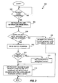
- FIG. 3 is a flow diagram of a memory card volume evaluation process 300 according to one embodiment of the invention.
- the memory card volume evaluation process 300 is, for example, performed by a host controller within a memory card.
- the host controller communicates with a host (host device) to read or write data to data storage components of the memory card.
- the memory card volume evaluation process 300 is initiated when a memory card is activated. Examples of activation of a memory card include (i) powering-on the memory card, or (ii) inserting the memory card into a receptacle of a host device. Initially, a decision 302 determines whether a memory card has been activated. When the decision 302 determines that a memory card has not been activated, then the memory card volume evaluation process 300 awaits such an event. In other words, the memory card volume evaluation process 300 can be invoked when a memory card is activated.
- volume information from an initial volume is retrieved 304.
- the initial volume is a volume (compatible with a file system) that is imposed on data storage components of the memory card.
- the memory card has previously been formatted for storage of files across one or more volumes. In the case where the memory card has only one volume, the one volume is the initial volume. In the case where the memory card has multiple volumes, the first volume is the initial volume.
- a decision 306 determines whether the volume information indicates that the compatible file system is less than or equal to a 16-bit file system. In other words, the decision 306 determines whether the file system is a file system for 16-bit (or less) addressing, i.e., FAT-16 (or less) formatted files.
- the host device is informed 308 that the memory card uses a single volume.
- the file system would then utilize 32-bit addressing and thus the file format for the single volume would be FAT-32 formatted files.
- a switch position is read 310.
- the memory card includes the switch 206 that is placed in one of a plurality of different switch positions.
- a decision 312 determines whether the switch position is in a first position. When the decision 312 determines that the switch position is not in a first position, then an appropriate address offset is set 314. In this case, the memory card is partitioned into multiple volumes, and when addressing those volumes other than the first volume, an appropriate address offset is utilized. Alternatively, following the decision 312 when the switch position is in the first position as well as following the operation 314, the host device is informed 316 to use the memory card as one of a plurality of selectable volumes with the appropriate address offset, if any. Here, the memory card does use a plurality of different volumes and the switch position is utilized to select one of the volumes, and, to the extent necessary, the appropriate address offset is provided. Following the operations 308 and 316, the memory card volume evaluation process 300 is complete and ends.
- FIG. 4 is a block diagram of a memory system 400 according to one embodiment of the invention.
- the memory system 400 represents, for example, a memory card (e.g., flash card).
- the memory system 400 is, for example, suitable for use as the memory card 102 shown in FIG. 1 or the memory card 200 shown in FIG. 2 .
- the memory system 400 includes a memory controller 402 and memory chips 404-410.
- the number of memory chips 404-410 is dependent upon the storage capacity to be provided by the conventional memory system 400 and the actual memory capacity of each memory chip.
- the memory controller 402 receives an Input/Output (I/O) bus 412.
- the memory controller 402 operates to supply an address/data/control bus 414 to each of the memory chips 404-410.
- the memory controller 402 produces a chip select (CS) signal 416 that is provided to chip enable (CE) terminals of each of the memory chips 404-410.
- the memory controller 402 uses the chip select signal 416 to selectively activate one of the memory chips 404-410 that is to be accessed for data storage or retrieval.
- the memory system 400 further includes a switch 418.
- the switch 418 has two or more switch positions that a user can choose from. Different switch positions are used to select different volumes. More particularly, the switch 418 provides an indication of its switch position to the memory controller 402. The memory controller 402 then operates the memory system 400 in accordance with the indication of the switch position.
- FIG. 5A is a diagram illustrating a single volume address space 500 suitable for use with the invention.
- the address space represents a two (2) gigabyte range of logical addresses from 000000 HEX through 7FFFFF HEX .
- volume information 502 contains at least an indication of whether the address space is configured as a FAT-16 file format.
- the address space covers a four (4) gigabyte range, and thus if a FAT-16 file format were to be utilized with this configuration, only 50% of the available data storage could be utilized.
- the address space 500 shown in FIG. 5A is suitable for use with a file system supporting thirty-two bit (32-bit) addressing (i.e., FAT-32 file format).
- FIG. 5B is a diagram of a multiple volume address space 520 suitable for use with the invention.
- the address space 520 also covers a four (4) gigabyte range, but is divided into a pair of two (2) gigabyte partitions. Namely, the address space 520 is divided into first and second two gigabyte regions. The first two gigabyte region extends from 000000 HEX to 3FFFFF HEX , and the second two gigabyte volume extends from 400000 HEX through 7FFFFF HEX .
- the first volume includes volume information 522 and host supplied data 524.
- the second volume includes volume information 526 and host-supplied data 528.
- 5B is suitable for use with a file system supporting sixteen bit (16-bit) addressing (i.e., FAT-16 file format).
- sixteen bit (16-bit) addressing i.e., FAT-16 file format.
- the host device When the address space 520 is utilized by an associated host device, the host device understands 16-bit addressing, i.e., the FAT-16 format, and can thus address either the first volume or the second volume.
- the switch such as the switch 206 shown in FIG. 2 , is utilized to cause the host to address either the first volume or the second volume.
- the host device and/or the memory card are able to understand the formatting previously applied to the memory card. For example, if the memory card were configured into first and second volumes similar to that shown in FIG. 5B , then upon reading the volume information 522, the host device and/or the memory card would understand that 16-bit addressing (i.e., the FAT-16 file format) is utilized. Hence, in such case, the host would thereafter access data storage associated with either the first volume or the second volume. In the case of using the second volume, an address offset would be utilized.
- 16-bit addressing i.e., the FAT-16 file format
- the host device and/or the memory card would understand that the memory card is formatted for 32-bit addressing, i.e., the FAT-32 file format. As a result, the host device could thereafter access data storage associated with a single volume covering its full range of storage capacity.
- the memory card provides interoperability with host devices supporting FAT-16 or FAT-32 file systems.
- host devices As the host devices become more complex and data-hungry, the ability to provide higher capacity memory cards is important. However, it is equally important that the interoperability between FAT-16 and FAT-32 systems be maintained.
- FIG. 6 is a diagram illustrating different configurations for an address space 600 of a memory card according to another embodiment of the invention.
- the different configurations represent three different volumes.
- the appropriate or desired one of the volumes can be selected by a switch position of a three-position switch for the memory card.
- the switch 206 can be the three-position switch in one embodiment.
- a first volume 602 has a two (2) gigabyte range of logical addresses from 000000 HEX through 3FFFFF HEX .
- the first volume can be selected by switch position A of the three-position switch for the memory card.
- a second volume 604 has a two (2) gigabyte range of logical addresses from 400000 HEX through 7FFFFF HEX .
- the second volume can be selected by switch position B of the switch for the memory card.
- a third volume 606 has a four (4) gigabyte range of logical addresses from 000000 HEX through 7FFFFF HEX .
- the third volume can be selected by switch position C of the three-position switch for the memory card.
- the volume can use FAT-16 or FAT-32 format.
- the volume must use a FAT-32 format.
- all three configurations can be invalid.
- the firmware determines whether to use FAT-16 or FAT-32 file format. In this embodiment, the firmware need not utilize system configuration information to determine the appropriate file format/volume.
- the firmware determines the appropriate file format/configuration for the memory card based on the switch position.
- the first volume can use logical addresses from 000000 HEX through 001023 HEX for system information in overall logical addresses from 004096 HEX through 005119 HEX, and can use logical addresses from 001024 HEX through 4001215 HEX for data in overall logical addresses from 006144 HEX through 4007359 HEX .
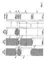
- FIG. 7 illustrates an alternate logical address to card logical address mapping that can also be used with a three position switch.
- the left column labeled SW A describes the mapping when the switch is in position A.
- Region 702 containing host addresses 000000 HEX through 0003FF HEX map into region 722 containing Card LBA's 001000 HEX through 0013FF HEX .
- This region is where the FAT-16 system information is stored.
- the second column labeled SW B shows that region 703 containing the FAT-16 system information for this volume maps into region 723 containing Card LBA's 001400 HEX through 0017FF HEX .
- the host mapping is shown in the column labeled SW C.
- Region 701 containing host addresses 000000 HEX through 000FFF HEX map into region 721 containing Card LBA's 000000 HEX through 000FFF HEX .
- the user data region 711, in this example extending from 001000 HEX through 7A2B7F HEX maps into regions 723, 724 and 725.
- One enhancement to this other embodiment is to have firmware assign the initial logical address space for the first and third volumes to different physical locations.
- the advantage of this enhancement allows the memory card to leave the factory with both FAT-16 and FAT-32 formats, thus being suitable for use by both newer and legacy systems and not requiring customer formatting.
- the integrated circuit packages according to the invention can be used in memory systems.
- the invention can further pertain to an electronic system that includes a memory system as discussed above.
- Memory systems are commonly used to store digital data for use with various electronics products. Often, the memory system is removable from the electronic system so that the stored digital data is portable. These memory systems can be referred to as memory cards.
- the memory systems according to the invention can have a relatively small form factor and can be used to store digital data for electronics products such as cameras, hand-held or notebook computers, network cards, network appliances, set-top boxes, hand-held or other small audio players/recorders (e.g., MP3 devices), and medical monitors.
- Examples of a memory card include PC Card (formerly PCMCIA device), Flash Card, Secure Digital (SD) Card, Multimedia Card (MMC card), and ATA Card (e.g., Compact Flash card).
- PC Card formerly PCMCIA device
- Flash Card Secure Digital (SD) Card
- MMC card Multimedia Card
- ATA Card e.g., Compact Flash card
- the memory card can use Flash type or EEPROM type memory cells to store the data.
- a memory system can pertain to a memory card (including a memory stick) or some other semiconductor memory product.
- One advantage of the invention is that a memory system can be used in a host device using 16-bit or 32-bit addressing.
- Another advantage of the invention is that automatic detection of the file format mitigates user errors and protects previously stored data.
- Still another advantage of the invention is that high density memory systems can be used in not only modern electronic products (using 32-bit addressing) but also legacy products (using 16-bit addressing).
Landscapes
- Engineering & Computer Science (AREA)
- Theoretical Computer Science (AREA)
- Physics & Mathematics (AREA)
- General Engineering & Computer Science (AREA)
- General Physics & Mathematics (AREA)
- Human Computer Interaction (AREA)
- Computer Security & Cryptography (AREA)
- Information Retrieval, Db Structures And Fs Structures Therefor (AREA)
- Techniques For Improving Reliability Of Storages (AREA)
- Memory System (AREA)
- Storage Device Security (AREA)
- Television Signal Processing For Recording (AREA)
- Closed-Circuit Television Systems (AREA)
- Traffic Control Systems (AREA)
- Communication Control (AREA)
Claims (17)
- Verfahren zum Lesen von Daten von einer Speicherkarte (200), welche einen nicht flüchtigen Datenspeicher bereitstellt, wobei das Verfahren umfasst:(a) Erfassen (304) einer Datenbereichsinformation (502, 522, 526) von einem ersten Datenbereich eines nicht flüchtigen Datenspeichers der Speicherkarte (200);(b) Bestimmen (306) abhängig von der Datenbereichsinformation (502, 522, 526), ob ein oder mehrere Datenbereiche auf der Speicherkarte (200) vorhanden sind;(c) Betreiben (316) der Speicherkarte (200), indem nur der erste Datenbereich bereitgestellt wird, wenn das Bestimmen (b) bestimmt, dass ein Datenbereich auf der Speicherkarte (200) vorhanden ist, wobei der nicht flüchtige Datenspeicher der Speicherkarte dem einen Datenbereich zugewiesen wird; und(d) Betreiben (316) der Speicherkarte (200), indem mehrere Datenbereiche bereitgestellt werden, wenn das Bestimmen (b) bestimmt, dass mehrere Datenbereiche auf der Speicherkarte (200) vorhanden sind, wobei einer der mehreren Datenbereiche der erste Datenbereich ist und der nicht flüchtige Datenspeicher unter den mehreren Datenbereichen aufgeteilt wird;wobei die Speicherkarte (200) einen Schalter (206) umfasst, welcher mehrere Schalterstellungen aufweist, und
wobei das Betreiben (316) (d) zumindest umfasst:(d1) Bestimmen einer Schalterstellung für den Schalter (206); und(d2) selektives Bereitstellen von einem der mehreren Datenbereiche abhängig von der Schalterstellung. - Verfahren nach Anspruch 1,
dadurch gekennzeichnet,
dass der Schalter (206) zumindest eine erste Stellung und eine zweite Stellung aufweist, und
dass das Betreiben (316) (d) darüber hinaus zumindest umfasst:(d3) Erstellen (314) eines Adressenversatzes, wenn sich der Schalter (206) in der zweiten Stellung befindet. - Verfahren nach Anspruch 2,
dadurch gekennzeichnet,
dass der Adressenversatz der Speicherkarte (200) ermöglicht, mehr Datenspeicherkapazität bereitzustellen, als mit einem Dateisystem, welches eine Adressierung mit 16 Bit einsetzt, möglich wäre. - Verfahren nach Anspruch 1,
dadurch gekennzeichnet,
dass der Schalter (206) zumindest eine erste Stellung und eine zweite Stellung aufweist,
dass, wenn sich die Schalterstellung in der ersten Stellung befindet und die Speicherkarte (200) betrieben wird, indem mehrere Datenbereiche bereitgestellt werden, auf den ersten Datenbereich des nicht flüchtigen Datenspeichers zugegriffen wird, und
dass, wenn sich die Schalterstellung in der zweiten Stellung befindet und die Speicherkarte (200) betrieben wird, indem mehrere Datenbereiche bereitgestellt werden, auf einen zweiten Datenbereich des nicht flüchtigen Datenspeichers zugegriffen wird. - Verfahren nach Anspruch 4,
dadurch gekennzeichnet,
dass die Speicherkarte (200) entweder als ein einziger Datenbereich oder als ein Datenbereichpaar formatiert wird, wobei das Datenbereichpaar von dem ersten Datenbereich und dem zweiten Datenbereich gebildet wird. - Verfahren nach Anspruch 5,
dadurch gekennzeichnet,
dass der gesamte nicht flüchtige Datenspeicher für die Speicherkarte (200) als der einzige Datenbereich in den ersten Datenbereich von X Gigabyte formatiert wird oder als das Datenbereichpaar in den ersten und den zweiten Datenbereich von jeweils X/2 Gigabyte formatiert wird. - Verfahren nach Anspruch 1,
dadurch gekennzeichnet,
dass das Verfahren darüber hinaus umfasst:(e) Erkennen (302) einer Aktivierung der Speicherkarte (200), und dass das Erfassen (304) (a), das Bestimmen (306) (b) und das Betreiben (316) (c) oder (d) durchgeführt werden, wenn das Erkennen (302) (e) die Aktivierung der Speicherkarte (200) einmal erkennt. - Verfahren nach Anspruch 7,
dadurch gekennzeichnet,
dass die Aktivierung der Speicherkarte (200) bei einem Einschalten der Speicherkarte (100) oder bei einer Einführung der Speicherkarte (200) in einen Hauptrechner (100) erfolgt. - Verfahren nach Anspruch 1,
dadurch gekennzeichnet,
dass die Speicherkarte (200) in einen einzigen Datenbereich oder in mehrere Datenbereiche formatiert wird, und
dass der gesamte nicht flüchtige Datenspeicher für die Speicherkarte (200) als der einzige Datenbereich in den ersten Datenbereich von X Gigabyte oder als mehrere Datenbereiche in die N Datenbereiche von jeweils X/N Gigabyte formatiert wird. - Verfahren nach Anspruch 1,
dadurch gekennzeichnet,
dass, wenn das Bestimmen (b) bestimmt, dass ein Datenbereich auf der Speicherkarte (200) vorhanden ist, der erste Datenbereich ein Dateiformat FAT-32 aufweist. - Verfahren nach Anspruch 1,
dadurch gekennzeichnet,
dass, wenn das Bestimmen (306) (b) bestimmt, dass mehrere Datenbereiche auf der Speicherkarte (200) vorhanden sind, jedes der mehreren Datenbereiche ein Dateiformat FAT-16 aufweist. - Speicherkarte (200), welche in der Lage ist, als einzelne Partition einer ersten Größe oder als mehrere Partitionen einer zweiten Größe konfiguriert zu werden, wobei die Speicherkarte (100) umfasst:einen nicht flüchtigen Datenspeicher (404, 406, 408, 410), welcher derart ausgestaltet ist, dass er einen Datenspeicher bereitstellt, wobei der nicht flüchtige Datenspeicher (404, 406, 408, 410) derart ausgestaltet ist, dass er zumindest eine erste Partition aufweist und eine Partitionsinformationen speichert, welche zumindest die erste Partition beschreibt;einen Schalter (206), welcher sich in einer von mehreren Schalterstellungen befindet; undeine Steuerung (402), welche einen Zugriff auf die Daten, welche in dem nicht flüchtigen Datenspeicher (404, 406, 408, 410) gespeichert sind, verwaltet,wobei die Steuerung (402) derart ausgestaltet ist, dass sie die Partitionsinformation, welche in dem nicht flüchtigen Datenspeicher (404, 406, 408, 410) gespeichert ist, auswertet, um abhängig von der Partitionsinformation zu bestimmen, ob die einzelne Partition oder die mehreren Partitionen eingesetzt werden,wobei, wenn die Steuerung (402) bestimmt, dass die einzelne Partition eingesetzt wird, der nicht flüchtige Datenspeicher als ein einziger Datenbereich adressiert wird, undwobei, wenn die Steuerung (402) bestimmt, dass die mehreren Partitionen eingesetzt werden, der nicht flüchtige Datenspeicher abhängig von der Schalterstellung des Schalters (206) als mehrere Partitionen adressiert wird.
- Speicherkarte (200) nach Anspruch 12,
dadurch gekennzeichnet,
dass die eine oder die mehreren Partitionen Datenbereiche sind. - Speicherkarte (200) nach Anspruch 12,
dadurch gekennzeichnet,
dass, wenn die Steuerung (402) bestimmt, dass die einzelne Partition auf der Speicherkarte (200) eingesetzt wird, die einzelne Partition ein Dateiformat FAT-32 aufweist. - Speicherkarte (200) nach Anspruch 12,
dadurch gekennzeichnet,
dass, wenn die Steuerung (402) bestimmt, dass die mehreren Partitionen eingesetzt werden, jede der mehreren Partitionen ein Dateiformat FAT-16 aufweist. - Speicherkarte (200) nach Anspruch 12,
dadurch gekennzeichnet,
dass die Speicherkarte (200) entweder als einzelne Partition oder als mehrere Partitionen formatiert wird, und
dass der gesamte nicht flüchtige Datenspeicher (404, 406, 408, 410) für die Speicherkarte (200) als die einzelne Partition für eine erste Partition von X Gigabyte formatiert wird oder als mehrere Partitionen in die N Partitionen von jeweils X/N Gigabyte formatiert wird. - Speicherkarte (200) nach Anspruch 12,
dadurch gekennzeichnet,
dass die Speicherkarte (200) ein FLASH-Speicherelement ist.
Priority Applications (1)
| Application Number | Priority Date | Filing Date | Title |
|---|---|---|---|
| EP09165816A EP2105829B1 (de) | 2004-01-09 | 2004-12-22 | Speicherkarte mit unterstützter Dateisystem-Interoperabilität |
Applications Claiming Priority (2)
| Application Number | Priority Date | Filing Date | Title |
|---|---|---|---|
| US10/754,483 US8001325B2 (en) | 2004-01-09 | 2004-01-09 | Memory card that supports file system interoperability |
| PCT/US2004/043683 WO2005071529A2 (en) | 2004-01-09 | 2004-12-22 | Memory card that supports file system interoperability |
Related Child Applications (1)
| Application Number | Title | Priority Date | Filing Date |
|---|---|---|---|
| EP09165816A Division EP2105829B1 (de) | 2004-01-09 | 2004-12-22 | Speicherkarte mit unterstützter Dateisystem-Interoperabilität |
Publications (2)
| Publication Number | Publication Date |
|---|---|
| EP1702260A2 EP1702260A2 (de) | 2006-09-20 |
| EP1702260B1 true EP1702260B1 (de) | 2009-09-30 |
Family
ID=34739403
Family Applications (2)
| Application Number | Title | Priority Date | Filing Date |
|---|---|---|---|
| EP09165816A Expired - Lifetime EP2105829B1 (de) | 2004-01-09 | 2004-12-22 | Speicherkarte mit unterstützter Dateisystem-Interoperabilität |
| EP04815698A Expired - Lifetime EP1702260B1 (de) | 2004-01-09 | 2004-12-22 | Speicherkarte die dateisysteminteroperabilität unterstützt |
Family Applications Before (1)
| Application Number | Title | Priority Date | Filing Date |
|---|---|---|---|
| EP09165816A Expired - Lifetime EP2105829B1 (de) | 2004-01-09 | 2004-12-22 | Speicherkarte mit unterstützter Dateisystem-Interoperabilität |
Country Status (9)
| Country | Link |
|---|---|
| US (1) | US8001325B2 (de) |
| EP (2) | EP2105829B1 (de) |
| JP (2) | JP5010922B2 (de) |
| KR (1) | KR20070006717A (de) |
| CN (1) | CN1934528B (de) |
| AT (2) | ATE444519T1 (de) |
| DE (1) | DE602004023425D1 (de) |
| TW (1) | TWI348640B (de) |
| WO (1) | WO2005071529A2 (de) |
Families Citing this family (17)
| Publication number | Priority date | Publication date | Assignee | Title |
|---|---|---|---|---|
| JP4515793B2 (ja) * | 2004-03-11 | 2010-08-04 | 株式会社東芝 | メモリカード装置およびメモリカード制御方法 |
| JP4541768B2 (ja) * | 2004-06-10 | 2010-09-08 | キヤノン株式会社 | 画像データ記録装置 |
| KR100770220B1 (ko) * | 2006-10-16 | 2007-10-26 | 삼성전자주식회사 | 메모리 카드 및 그 제조 방법 |
| US7966355B2 (en) * | 2007-02-13 | 2011-06-21 | Modu Ltd. | Interface for extending functionality of memory cards |
| US20080277485A1 (en) * | 2007-05-07 | 2008-11-13 | Samsung Electronics Co., Ltd. | Memory card having multiple application-based functions, method of manufacturing the same, method of operating the same and digital device applying the same |
| WO2009016832A1 (ja) | 2007-07-31 | 2009-02-05 | Panasonic Corporation | 不揮発性記憶装置および不揮発性記憶システム |
| US8312247B2 (en) * | 2008-06-20 | 2012-11-13 | Panasonic Corporation | Plural-partitioned type nonvolatile storage device and system |
| US20100318720A1 (en) * | 2009-06-16 | 2010-12-16 | Saranyan Rajagopalan | Multi-Bank Non-Volatile Memory System with Satellite File System |
| CN107093464A (zh) | 2010-07-13 | 2017-08-25 | 桑迪士克科技有限责任公司 | 后台存储器系统接口的动态优化 |
| US8464135B2 (en) | 2010-07-13 | 2013-06-11 | Sandisk Technologies Inc. | Adaptive flash interface |
| US9069688B2 (en) | 2011-04-15 | 2015-06-30 | Sandisk Technologies Inc. | Dynamic optimization of back-end memory system interface |
| US8856482B2 (en) | 2011-03-11 | 2014-10-07 | Micron Technology, Inc. | Systems, devices, memory controllers, and methods for memory initialization |
| US8462536B2 (en) * | 2011-03-11 | 2013-06-11 | Intel Corporation | Method and apparatus for addressing memory arrays |
| US10053282B2 (en) | 2012-10-24 | 2018-08-21 | Munchkin, Inc. | Cassette for dispensing pleated tubing |
| US9141291B2 (en) | 2013-11-26 | 2015-09-22 | Sandisk Technologies Inc. | Adaptive context disbursement for improved performance in non-volatile memory systems |
| US9384128B2 (en) | 2014-04-18 | 2016-07-05 | SanDisk Technologies, Inc. | Multi-level redundancy code for non-volatile memory controller |
| US11163442B2 (en) * | 2019-12-08 | 2021-11-02 | Western Digital Technologies, Inc. | Self-formatting data storage device |
Family Cites Families (20)
| Publication number | Priority date | Publication date | Assignee | Title |
|---|---|---|---|---|
| JPH07141479A (ja) * | 1993-11-18 | 1995-06-02 | Toshiba Corp | Icメモリカードおよびそのicメモリカードを使用したファイル管理システム |
| US5860082A (en) | 1996-03-28 | 1999-01-12 | Datalight, Inc. | Method and apparatus for allocating storage in a flash memory |
| JP3274604B2 (ja) | 1996-04-26 | 2002-04-15 | インターナショナル・ビジネス・マシーンズ・コーポレーション | 周辺デバイスの自動イネーブル方法 |
| JPH1021123A (ja) * | 1996-07-02 | 1998-01-23 | Nissin Electric Co Ltd | 情報処理装置 |
| JPH10171938A (ja) * | 1996-12-05 | 1998-06-26 | Hitachi Maxell Ltd | Pcカード |
| JP3159150B2 (ja) * | 1997-11-27 | 2001-04-23 | 株式会社村田製作所 | Pcカード |
| GB9813830D0 (en) * | 1998-06-27 | 1998-08-26 | Philips Electronics Nv | Flexible management of multiple file systems |
| US6275894B1 (en) | 1998-09-23 | 2001-08-14 | Advanced Micro Devices, Inc. | Bank selector circuit for a simultaneous operation flash memory device with a flexible bank partition architecture |
| US6519762B1 (en) * | 1998-12-15 | 2003-02-11 | Dell Usa, L.P. | Method and apparatus for restoration of a computer system hard drive |
| US6654772B1 (en) * | 1999-04-28 | 2003-11-25 | Emc Corporation | Multi-volume extent based file system |
| US6185666B1 (en) * | 1999-09-11 | 2001-02-06 | Powerquest Corporation | Merging computer partitions |
| US6715067B1 (en) * | 1999-09-21 | 2004-03-30 | Intel Corporation | Initializing a processor-based system from a non-volatile re-programmable semiconductor memory |
| JP4556285B2 (ja) * | 2000-04-24 | 2010-10-06 | ソニー株式会社 | 記録再生装置 |
| JP3942807B2 (ja) | 2000-06-06 | 2007-07-11 | 株式会社ルネサステクノロジ | ブロックアラインメント機能付き半導体記憶装置 |
| JP4403647B2 (ja) | 2000-09-05 | 2010-01-27 | ソニー株式会社 | 記録媒体カード及びその製造方法 |
| US7062616B2 (en) | 2001-06-12 | 2006-06-13 | Intel Corporation | Implementing a dual partition flash with suspend/resume capabilities |
| TW531752B (en) | 2001-11-23 | 2003-05-11 | Key Technology Corp | Method for automatic file setup system in a flash memory storage device |
| KR100499686B1 (ko) * | 2002-07-23 | 2005-07-07 | 주식회사 디지털웨이 | 메모리 확장 가능한 휴대용 플래쉬 메모리 장치 |
| JP3806077B2 (ja) * | 2002-08-26 | 2006-08-09 | 株式会社東芝 | メモリカード認識システム、容量切り替え型メモリカード・ホスト機器、容量切り替え型メモリカード、記憶容量設定方法及び記憶容量設定プログラム |
| JP3866635B2 (ja) * | 2002-08-26 | 2007-01-10 | 株式会社東芝 | メモリカード及び記憶領域切り替え方法 |
-
2004
- 2004-01-09 US US10/754,483 patent/US8001325B2/en not_active Expired - Lifetime
- 2004-12-22 DE DE602004023425T patent/DE602004023425D1/de not_active Expired - Lifetime
- 2004-12-22 JP JP2006549320A patent/JP5010922B2/ja not_active Expired - Fee Related
- 2004-12-22 KR KR1020067015188A patent/KR20070006717A/ko not_active Withdrawn
- 2004-12-22 WO PCT/US2004/043683 patent/WO2005071529A2/en not_active Ceased
- 2004-12-22 CN CN2004800422135A patent/CN1934528B/zh not_active Expired - Fee Related
- 2004-12-22 AT AT04815698T patent/ATE444519T1/de not_active IP Right Cessation
- 2004-12-22 EP EP09165816A patent/EP2105829B1/de not_active Expired - Lifetime
- 2004-12-22 AT AT09165816T patent/ATE535858T1/de active
- 2004-12-22 EP EP04815698A patent/EP1702260B1/de not_active Expired - Lifetime
-
2005
- 2005-01-06 TW TW094100402A patent/TWI348640B/zh not_active IP Right Cessation
-
2011
- 2011-12-27 JP JP2011286244A patent/JP5405556B2/ja not_active Expired - Fee Related
Also Published As
| Publication number | Publication date |
|---|---|
| TWI348640B (en) | 2011-09-11 |
| KR20070006717A (ko) | 2007-01-11 |
| US20050154819A1 (en) | 2005-07-14 |
| WO2005071529A3 (en) | 2005-12-15 |
| JP5405556B2 (ja) | 2014-02-05 |
| ATE444519T1 (de) | 2009-10-15 |
| ATE535858T1 (de) | 2011-12-15 |
| US8001325B2 (en) | 2011-08-16 |
| EP2105829A1 (de) | 2009-09-30 |
| WO2005071529A2 (en) | 2005-08-04 |
| JP2012084170A (ja) | 2012-04-26 |
| JP2007518188A (ja) | 2007-07-05 |
| EP2105829B1 (de) | 2011-11-30 |
| CN1934528A (zh) | 2007-03-21 |
| CN1934528B (zh) | 2011-05-04 |
| DE602004023425D1 (de) | 2009-11-12 |
| JP5010922B2 (ja) | 2012-08-29 |
| TW200540690A (en) | 2005-12-16 |
| EP1702260A2 (de) | 2006-09-20 |
Similar Documents
| Publication | Publication Date | Title |
|---|---|---|
| JP5405556B2 (ja) | ファイルシステム相互運用性をサポートするメモリカードおよび方法 | |
| US6839864B2 (en) | Field-operable, stand-alone apparatus for media recovery and regeneration | |
| US7039754B2 (en) | Detachably mounted removable data storage device | |
| US7007127B2 (en) | Method and related apparatus for controlling transmission interface between an external device and a computer system | |
| US7278051B2 (en) | Field-operable, stand-alone apparatus for media recovery and regeneration | |
| KR100975178B1 (ko) | 데이터 기억 장치 | |
| EP1920317B1 (de) | Massendatenspeichersystem | |
| US20030177300A1 (en) | Data processing method in high-capacity flash EEPROM card system | |
| US5761732A (en) | Interleaving for memory cards | |
| KR20080032636A (ko) | 논리 어드레스 공간 전반에 걸쳐 그리고 직접 데이터 파일기반 위에서 동작하는 인터페이싱 시스템 | |
| US20060087957A1 (en) | Format mapping scheme for universal drive device | |
| EP2370914A1 (de) | Speicheranordnung, die hosts nur mit einer definierten hostfähigkeit kompatible dateien präsentiert | |
| JPH09147545A (ja) | メモリカードおよび情報処理装置 | |
| US12277334B2 (en) | Selectable performance-based partitioning | |
| US20050092846A1 (en) | Simulated smartmedia/XD-picture memory card capable of using various kinds on non-volatile memory | |
| US20100115319A1 (en) | Storing device and electronic device having the same | |
| US20040230789A1 (en) | Multi memory card accessing system and implementation method thereof | |
| JPH07141479A (ja) | Icメモリカードおよびそのicメモリカードを使用したファイル管理システム | |
| EP0193306A2 (de) | Festkörperspeicherkassette | |
| EP1618464A1 (de) | Partitionsauswahl für universelles speichergerät | |
| KR20060095133A (ko) | 비휘발성 메모리에 저장된 시스템 프로그램을 구동시키는방법 | |
| JPH05225406A (ja) | Icカード拡張装置 | |
| Kimball | Cutting-edge digital storage for portable imaging systems | |
| GB2253929A (en) | Disk drive emulation |
Legal Events
| Date | Code | Title | Description |
|---|---|---|---|
| PUAI | Public reference made under article 153(3) epc to a published international application that has entered the european phase |
Free format text: ORIGINAL CODE: 0009012 |
|
| 17P | Request for examination filed |
Effective date: 20060712 |
|
| AK | Designated contracting states |
Kind code of ref document: A2 Designated state(s): AT BE BG CH CY CZ DE DK EE ES FI FR GB GR HU IE IS IT LI LT LU MC NL PL PT RO SE SI SK TR |
|
| 17Q | First examination report despatched |
Effective date: 20070212 |
|
| DAX | Request for extension of the european patent (deleted) | ||
| GRAP | Despatch of communication of intention to grant a patent |
Free format text: ORIGINAL CODE: EPIDOSNIGR1 |
|
| GRAS | Grant fee paid |
Free format text: ORIGINAL CODE: EPIDOSNIGR3 |
|
| GRAA | (expected) grant |
Free format text: ORIGINAL CODE: 0009210 |
|
| RIN1 | Information on inventor provided before grant (corrected) |
Inventor name: CEDAR, YORAM Inventor name: BONE, ERIC Inventor name: CONLEY, KEVIN Inventor name: BREWER, WES, G. Inventor name: CHANG, ROBERT |
|
| AK | Designated contracting states |
Kind code of ref document: B1 Designated state(s): AT BE BG CH CY CZ DE DK EE ES FI FR GB GR HU IE IS IT LI LT LU MC NL PL PT RO SE SI SK TR |
|
| REG | Reference to a national code |
Ref country code: CH Ref legal event code: EP Ref country code: GB Ref legal event code: FG4D |
|
| REG | Reference to a national code |
Ref country code: IE Ref legal event code: FG4D |
|
| REF | Corresponds to: |
Ref document number: 602004023425 Country of ref document: DE Date of ref document: 20091112 Kind code of ref document: P |
|
| PG25 | Lapsed in a contracting state [announced via postgrant information from national office to epo] |
Ref country code: LT Free format text: LAPSE BECAUSE OF FAILURE TO SUBMIT A TRANSLATION OF THE DESCRIPTION OR TO PAY THE FEE WITHIN THE PRESCRIBED TIME-LIMIT Effective date: 20090930 Ref country code: SE Free format text: LAPSE BECAUSE OF FAILURE TO SUBMIT A TRANSLATION OF THE DESCRIPTION OR TO PAY THE FEE WITHIN THE PRESCRIBED TIME-LIMIT Effective date: 20090930 Ref country code: FI Free format text: LAPSE BECAUSE OF FAILURE TO SUBMIT A TRANSLATION OF THE DESCRIPTION OR TO PAY THE FEE WITHIN THE PRESCRIBED TIME-LIMIT Effective date: 20090930 |
|
| LTIE | Lt: invalidation of european patent or patent extension |
Effective date: 20090930 |
|
| PG25 | Lapsed in a contracting state [announced via postgrant information from national office to epo] |
Ref country code: PL Free format text: LAPSE BECAUSE OF FAILURE TO SUBMIT A TRANSLATION OF THE DESCRIPTION OR TO PAY THE FEE WITHIN THE PRESCRIBED TIME-LIMIT Effective date: 20090930 Ref country code: SI Free format text: LAPSE BECAUSE OF FAILURE TO SUBMIT A TRANSLATION OF THE DESCRIPTION OR TO PAY THE FEE WITHIN THE PRESCRIBED TIME-LIMIT Effective date: 20090930 |
|
| PG25 | Lapsed in a contracting state [announced via postgrant information from national office to epo] |
Ref country code: CZ Free format text: LAPSE BECAUSE OF FAILURE TO SUBMIT A TRANSLATION OF THE DESCRIPTION OR TO PAY THE FEE WITHIN THE PRESCRIBED TIME-LIMIT Effective date: 20090930 Ref country code: PT Free format text: LAPSE BECAUSE OF FAILURE TO SUBMIT A TRANSLATION OF THE DESCRIPTION OR TO PAY THE FEE WITHIN THE PRESCRIBED TIME-LIMIT Effective date: 20100201 Ref country code: IS Free format text: LAPSE BECAUSE OF FAILURE TO SUBMIT A TRANSLATION OF THE DESCRIPTION OR TO PAY THE FEE WITHIN THE PRESCRIBED TIME-LIMIT Effective date: 20100130 Ref country code: EE Free format text: LAPSE BECAUSE OF FAILURE TO SUBMIT A TRANSLATION OF THE DESCRIPTION OR TO PAY THE FEE WITHIN THE PRESCRIBED TIME-LIMIT Effective date: 20090930 Ref country code: RO Free format text: LAPSE BECAUSE OF FAILURE TO SUBMIT A TRANSLATION OF THE DESCRIPTION OR TO PAY THE FEE WITHIN THE PRESCRIBED TIME-LIMIT Effective date: 20090930 Ref country code: ES Free format text: LAPSE BECAUSE OF FAILURE TO SUBMIT A TRANSLATION OF THE DESCRIPTION OR TO PAY THE FEE WITHIN THE PRESCRIBED TIME-LIMIT Effective date: 20100110 |
|
| PG25 | Lapsed in a contracting state [announced via postgrant information from national office to epo] |
Ref country code: CY Free format text: LAPSE BECAUSE OF FAILURE TO SUBMIT A TRANSLATION OF THE DESCRIPTION OR TO PAY THE FEE WITHIN THE PRESCRIBED TIME-LIMIT Effective date: 20090930 Ref country code: SK Free format text: LAPSE BECAUSE OF FAILURE TO SUBMIT A TRANSLATION OF THE DESCRIPTION OR TO PAY THE FEE WITHIN THE PRESCRIBED TIME-LIMIT Effective date: 20090930 |
|
| PG25 | Lapsed in a contracting state [announced via postgrant information from national office to epo] |
Ref country code: BE Free format text: LAPSE BECAUSE OF FAILURE TO SUBMIT A TRANSLATION OF THE DESCRIPTION OR TO PAY THE FEE WITHIN THE PRESCRIBED TIME-LIMIT Effective date: 20090930 Ref country code: AT Free format text: LAPSE BECAUSE OF FAILURE TO SUBMIT A TRANSLATION OF THE DESCRIPTION OR TO PAY THE FEE WITHIN THE PRESCRIBED TIME-LIMIT Effective date: 20090930 |
|
| PG25 | Lapsed in a contracting state [announced via postgrant information from national office to epo] |
Ref country code: MC Free format text: LAPSE BECAUSE OF NON-PAYMENT OF DUE FEES Effective date: 20100701 Ref country code: DK Free format text: LAPSE BECAUSE OF FAILURE TO SUBMIT A TRANSLATION OF THE DESCRIPTION OR TO PAY THE FEE WITHIN THE PRESCRIBED TIME-LIMIT Effective date: 20090930 |
|
| REG | Reference to a national code |
Ref country code: CH Ref legal event code: PL |
|
| PLBE | No opposition filed within time limit |
Free format text: ORIGINAL CODE: 0009261 |
|
| STAA | Information on the status of an ep patent application or granted ep patent |
Free format text: STATUS: NO OPPOSITION FILED WITHIN TIME LIMIT |
|
| GBPC | Gb: european patent ceased through non-payment of renewal fee |
Effective date: 20091230 |
|
| 26N | No opposition filed |
Effective date: 20100701 |
|
| PG25 | Lapsed in a contracting state [announced via postgrant information from national office to epo] |
Ref country code: LI Free format text: LAPSE BECAUSE OF NON-PAYMENT OF DUE FEES Effective date: 20091231 Ref country code: CH Free format text: LAPSE BECAUSE OF NON-PAYMENT OF DUE FEES Effective date: 20091231 Ref country code: GR Free format text: LAPSE BECAUSE OF FAILURE TO SUBMIT A TRANSLATION OF THE DESCRIPTION OR TO PAY THE FEE WITHIN THE PRESCRIBED TIME-LIMIT Effective date: 20091231 Ref country code: IE Free format text: LAPSE BECAUSE OF NON-PAYMENT OF DUE FEES Effective date: 20091222 |
|
| PG25 | Lapsed in a contracting state [announced via postgrant information from national office to epo] |
Ref country code: GB Free format text: LAPSE BECAUSE OF NON-PAYMENT OF DUE FEES Effective date: 20091230 |
|
| PG25 | Lapsed in a contracting state [announced via postgrant information from national office to epo] |
Ref country code: BG Free format text: LAPSE BECAUSE OF FAILURE TO SUBMIT A TRANSLATION OF THE DESCRIPTION OR TO PAY THE FEE WITHIN THE PRESCRIBED TIME-LIMIT Effective date: 20091231 Ref country code: IT Free format text: LAPSE BECAUSE OF FAILURE TO SUBMIT A TRANSLATION OF THE DESCRIPTION OR TO PAY THE FEE WITHIN THE PRESCRIBED TIME-LIMIT Effective date: 20090930 |
|
| PG25 | Lapsed in a contracting state [announced via postgrant information from national office to epo] |
Ref country code: LU Free format text: LAPSE BECAUSE OF NON-PAYMENT OF DUE FEES Effective date: 20091222 |
|
| PG25 | Lapsed in a contracting state [announced via postgrant information from national office to epo] |
Ref country code: HU Free format text: LAPSE BECAUSE OF FAILURE TO SUBMIT A TRANSLATION OF THE DESCRIPTION OR TO PAY THE FEE WITHIN THE PRESCRIBED TIME-LIMIT Effective date: 20100401 |
|
| PG25 | Lapsed in a contracting state [announced via postgrant information from national office to epo] |
Ref country code: TR Free format text: LAPSE BECAUSE OF FAILURE TO SUBMIT A TRANSLATION OF THE DESCRIPTION OR TO PAY THE FEE WITHIN THE PRESCRIBED TIME-LIMIT Effective date: 20090930 |
|
| REG | Reference to a national code |
Ref country code: NL Ref legal event code: SD Effective date: 20111229 |
|
| REG | Reference to a national code |
Ref country code: DE Ref legal event code: R082 Ref document number: 602004023425 Country of ref document: DE Representative=s name: PATENT- UND RECHTSANWAELTE KRAUS & WEISERT, DE |
|
| REG | Reference to a national code |
Ref country code: DE Ref legal event code: R082 Ref document number: 602004023425 Country of ref document: DE Representative=s name: KRAUS & WEISERT PATENTANWAELTE PARTGMBB, DE Effective date: 20120713 Ref country code: DE Ref legal event code: R081 Ref document number: 602004023425 Country of ref document: DE Owner name: SANDISK TECHNOLOGIES INC., PLANO, US Free format text: FORMER OWNER: SANDISK CORP., SUNNYVALE, CALIF., US Effective date: 20120713 Ref country code: DE Ref legal event code: R081 Ref document number: 602004023425 Country of ref document: DE Owner name: SANDISK TECHNOLOGIES INC., US Free format text: FORMER OWNER: SANDISK CORP., SUNNYVALE, US Effective date: 20120713 Ref country code: DE Ref legal event code: R082 Ref document number: 602004023425 Country of ref document: DE Representative=s name: PATENT- UND RECHTSANWAELTE KRAUS & WEISERT, DE Effective date: 20120713 Ref country code: DE Ref legal event code: R081 Ref document number: 602004023425 Country of ref document: DE Owner name: SANDISK TECHNOLOGIES LLC, PLANO, US Free format text: FORMER OWNER: SANDISK CORP., SUNNYVALE, CALIF., US Effective date: 20120713 |
|
| PGFP | Annual fee paid to national office [announced via postgrant information from national office to epo] |
Ref country code: FR Payment date: 20131209 Year of fee payment: 10 |
|
| REG | Reference to a national code |
Ref country code: FR Ref legal event code: ST Effective date: 20150831 |
|
| PG25 | Lapsed in a contracting state [announced via postgrant information from national office to epo] |
Ref country code: FR Free format text: LAPSE BECAUSE OF NON-PAYMENT OF DUE FEES Effective date: 20141231 |
|
| REG | Reference to a national code |
Ref country code: DE Ref legal event code: R082 Ref document number: 602004023425 Country of ref document: DE Representative=s name: KRAUS & WEISERT PATENTANWAELTE PARTGMBB, DE Ref country code: DE Ref legal event code: R081 Ref document number: 602004023425 Country of ref document: DE Owner name: SANDISK TECHNOLOGIES LLC, PLANO, US Free format text: FORMER OWNER: SANDISK TECHNOLOGIES INC., PLANO, TEX., US |
|
| PGFP | Annual fee paid to national office [announced via postgrant information from national office to epo] |
Ref country code: NL Payment date: 20221114 Year of fee payment: 19 Ref country code: DE Payment date: 20221025 Year of fee payment: 19 |
|
| P01 | Opt-out of the competence of the unified patent court (upc) registered |
Effective date: 20230606 |
|
| REG | Reference to a national code |
Ref country code: DE Ref legal event code: R119 Ref document number: 602004023425 Country of ref document: DE |
|
| REG | Reference to a national code |
Ref country code: NL Ref legal event code: MM Effective date: 20240101 |
|
| PG25 | Lapsed in a contracting state [announced via postgrant information from national office to epo] |
Ref country code: NL Free format text: LAPSE BECAUSE OF NON-PAYMENT OF DUE FEES Effective date: 20240101 |
|
| PG25 | Lapsed in a contracting state [announced via postgrant information from national office to epo] |
Ref country code: NL Free format text: LAPSE BECAUSE OF NON-PAYMENT OF DUE FEES Effective date: 20240101 |
|
| PG25 | Lapsed in a contracting state [announced via postgrant information from national office to epo] |
Ref country code: DE Free format text: LAPSE BECAUSE OF NON-PAYMENT OF DUE FEES Effective date: 20240702 |
|
| PG25 | Lapsed in a contracting state [announced via postgrant information from national office to epo] |
Ref country code: DE Free format text: LAPSE BECAUSE OF NON-PAYMENT OF DUE FEES Effective date: 20240702 |