EP1705016A2 - Actuateur piézo-électrique, tête à jet d'encre, méthode de production d'un actuateur piézo-électrique et méthode de production d'une tête à jet d'encre - Google Patents
Actuateur piézo-électrique, tête à jet d'encre, méthode de production d'un actuateur piézo-électrique et méthode de production d'une tête à jet d'encre Download PDFInfo
- Publication number
- EP1705016A2 EP1705016A2 EP06005758A EP06005758A EP1705016A2 EP 1705016 A2 EP1705016 A2 EP 1705016A2 EP 06005758 A EP06005758 A EP 06005758A EP 06005758 A EP06005758 A EP 06005758A EP 1705016 A2 EP1705016 A2 EP 1705016A2
- Authority
- EP
- European Patent Office
- Prior art keywords
- piezoelectric
- electrode layer
- ink
- forming
- piezoelectric layer
- Prior art date
- Legal status (The legal status is an assumption and is not a legal conclusion. Google has not performed a legal analysis and makes no representation as to the accuracy of the status listed.)
- Granted
Links
- 238000000034 method Methods 0.000 title claims abstract description 39
- 239000000443 aerosol Substances 0.000 claims abstract description 44
- 239000000463 material Substances 0.000 claims abstract description 38
- 238000001354 calcination Methods 0.000 claims abstract description 37
- 238000000137 annealing Methods 0.000 claims abstract description 34
- 239000004020 conductor Substances 0.000 claims abstract description 22
- 239000002082 metal nanoparticle Substances 0.000 claims abstract description 19
- 239000002245 particle Substances 0.000 claims description 65
- 239000000758 substrate Substances 0.000 claims description 26
- 229910052751 metal Inorganic materials 0.000 claims description 7
- 239000002184 metal Substances 0.000 claims description 7
- 229910052709 silver Inorganic materials 0.000 claims description 7
- 239000004332 silver Substances 0.000 claims description 7
- 238000007664 blowing Methods 0.000 claims description 6
- 238000007599 discharging Methods 0.000 claims 2
- 238000000151 deposition Methods 0.000 abstract description 16
- 230000015556 catabolic process Effects 0.000 abstract description 6
- 238000006731 degradation reaction Methods 0.000 abstract description 6
- 238000009792 diffusion process Methods 0.000 abstract description 6
- 238000004299 exfoliation Methods 0.000 abstract description 5
- 239000010408 film Substances 0.000 description 13
- 238000004519 manufacturing process Methods 0.000 description 7
- 238000005245 sintering Methods 0.000 description 7
- 229910001220 stainless steel Inorganic materials 0.000 description 7
- 239000010935 stainless steel Substances 0.000 description 7
- 230000015572 biosynthetic process Effects 0.000 description 6
- 229910052451 lead zirconate titanate Inorganic materials 0.000 description 6
- 239000002923 metal particle Substances 0.000 description 6
- BQCADISMDOOEFD-UHFFFAOYSA-N Silver Chemical compound [Ag] BQCADISMDOOEFD-UHFFFAOYSA-N 0.000 description 5
- 238000002441 X-ray diffraction Methods 0.000 description 5
- 239000012159 carrier gas Substances 0.000 description 5
- 238000010586 diagram Methods 0.000 description 5
- 238000002844 melting Methods 0.000 description 5
- 239000007789 gas Substances 0.000 description 4
- 238000010438 heat treatment Methods 0.000 description 4
- 230000008018 melting Effects 0.000 description 4
- BASFCYQUMIYNBI-UHFFFAOYSA-N platinum Substances [Pt] BASFCYQUMIYNBI-UHFFFAOYSA-N 0.000 description 4
- 238000001228 spectrum Methods 0.000 description 4
- FOIXSVOLVBLSDH-UHFFFAOYSA-N Silver ion Chemical compound [Ag+] FOIXSVOLVBLSDH-UHFFFAOYSA-N 0.000 description 3
- 238000007906 compression Methods 0.000 description 3
- 230000003247 decreasing effect Effects 0.000 description 3
- 230000000694 effects Effects 0.000 description 3
- 230000005684 electric field Effects 0.000 description 3
- HFGPZNIAWCZYJU-UHFFFAOYSA-N lead zirconate titanate Chemical compound [O-2].[O-2].[O-2].[O-2].[O-2].[Ti+4].[Zr+4].[Pb+2] HFGPZNIAWCZYJU-UHFFFAOYSA-N 0.000 description 3
- 239000002105 nanoparticle Substances 0.000 description 3
- 229920003002 synthetic resin Polymers 0.000 description 3
- 239000000057 synthetic resin Substances 0.000 description 3
- 239000010409 thin film Substances 0.000 description 3
- XKRFYHLGVUSROY-UHFFFAOYSA-N Argon Chemical compound [Ar] XKRFYHLGVUSROY-UHFFFAOYSA-N 0.000 description 2
- IJGRMHOSHXDMSA-UHFFFAOYSA-N Atomic nitrogen Chemical compound N#N IJGRMHOSHXDMSA-UHFFFAOYSA-N 0.000 description 2
- 239000011248 coating agent Substances 0.000 description 2
- 238000000576 coating method Methods 0.000 description 2
- 239000007772 electrode material Substances 0.000 description 2
- 238000005530 etching Methods 0.000 description 2
- PCHJSUWPFVWCPO-UHFFFAOYSA-N gold Chemical compound [Au] PCHJSUWPFVWCPO-UHFFFAOYSA-N 0.000 description 2
- 229910052737 gold Inorganic materials 0.000 description 2
- 239000010931 gold Substances 0.000 description 2
- 239000007769 metal material Substances 0.000 description 2
- 230000010287 polarization Effects 0.000 description 2
- 238000003980 solgel method Methods 0.000 description 2
- 239000000126 substance Substances 0.000 description 2
- 239000004593 Epoxy Substances 0.000 description 1
- 239000004642 Polyimide Substances 0.000 description 1
- 239000000853 adhesive Substances 0.000 description 1
- 230000001070 adhesive effect Effects 0.000 description 1
- 229910052786 argon Inorganic materials 0.000 description 1
- QVGXLLKOCUKJST-UHFFFAOYSA-N atomic oxygen Chemical compound [O] QVGXLLKOCUKJST-UHFFFAOYSA-N 0.000 description 1
- 239000000919 ceramic Substances 0.000 description 1
- 238000010276 construction Methods 0.000 description 1
- 230000000593 degrading effect Effects 0.000 description 1
- 239000002270 dispersing agent Substances 0.000 description 1
- 238000001035 drying Methods 0.000 description 1
- 238000004134 energy conservation Methods 0.000 description 1
- -1 for example Substances 0.000 description 1
- 239000001307 helium Substances 0.000 description 1
- 229910052734 helium Inorganic materials 0.000 description 1
- SWQJXJOGLNCZEY-UHFFFAOYSA-N helium atom Chemical compound [He] SWQJXJOGLNCZEY-UHFFFAOYSA-N 0.000 description 1
- 239000011261 inert gas Substances 0.000 description 1
- 238000007641 inkjet printing Methods 0.000 description 1
- 238000005304 joining Methods 0.000 description 1
- 238000011068 loading method Methods 0.000 description 1
- 238000005259 measurement Methods 0.000 description 1
- 238000002156 mixing Methods 0.000 description 1
- 229910052757 nitrogen Inorganic materials 0.000 description 1
- 229910052574 oxide ceramic Inorganic materials 0.000 description 1
- 239000011224 oxide ceramic Substances 0.000 description 1
- 239000001301 oxygen Substances 0.000 description 1
- 229910052760 oxygen Inorganic materials 0.000 description 1
- 229910052697 platinum Inorganic materials 0.000 description 1
- 229920001721 polyimide Polymers 0.000 description 1
- 239000000843 powder Substances 0.000 description 1
- 238000007639 printing Methods 0.000 description 1
- 238000011084 recovery Methods 0.000 description 1
- 238000000611 regression analysis Methods 0.000 description 1
- 238000007650 screen-printing Methods 0.000 description 1
- 238000004544 sputter deposition Methods 0.000 description 1
- 229920001187 thermosetting polymer Polymers 0.000 description 1
Images


Classifications
-
- B—PERFORMING OPERATIONS; TRANSPORTING
- B41—PRINTING; LINING MACHINES; TYPEWRITERS; STAMPS
- B41J—TYPEWRITERS; SELECTIVE PRINTING MECHANISMS, i.e. MECHANISMS PRINTING OTHERWISE THAN FROM A FORME; CORRECTION OF TYPOGRAPHICAL ERRORS
- B41J2/00—Typewriters or selective printing mechanisms characterised by the printing or marking process for which they are designed
- B41J2/005—Typewriters or selective printing mechanisms characterised by the printing or marking process for which they are designed characterised by bringing liquid or particles selectively into contact with a printing material
- B41J2/01—Ink jet
- B41J2/135—Nozzles
- B41J2/16—Production of nozzles
- B41J2/1607—Production of print heads with piezoelectric elements
- B41J2/161—Production of print heads with piezoelectric elements of film type, deformed by bending and disposed on a diaphragm
-
- B—PERFORMING OPERATIONS; TRANSPORTING
- B41—PRINTING; LINING MACHINES; TYPEWRITERS; STAMPS
- B41J—TYPEWRITERS; SELECTIVE PRINTING MECHANISMS, i.e. MECHANISMS PRINTING OTHERWISE THAN FROM A FORME; CORRECTION OF TYPOGRAPHICAL ERRORS
- B41J2/00—Typewriters or selective printing mechanisms characterised by the printing or marking process for which they are designed
- B41J2/005—Typewriters or selective printing mechanisms characterised by the printing or marking process for which they are designed characterised by bringing liquid or particles selectively into contact with a printing material
- B41J2/01—Ink jet
- B41J2/135—Nozzles
- B41J2/16—Production of nozzles
- B41J2/1621—Manufacturing processes
- B41J2/1623—Manufacturing processes bonding and adhesion
-
- H—ELECTRICITY
- H10—SEMICONDUCTOR DEVICES; ELECTRIC SOLID-STATE DEVICES NOT OTHERWISE PROVIDED FOR
- H10N—ELECTRIC SOLID-STATE DEVICES NOT OTHERWISE PROVIDED FOR
- H10N30/00—Piezoelectric or electrostrictive devices
- H10N30/01—Manufacture or treatment
- H10N30/07—Forming of piezoelectric or electrostrictive parts or bodies on an electrical element or another base
- H10N30/074—Forming of piezoelectric or electrostrictive parts or bodies on an electrical element or another base by depositing piezoelectric or electrostrictive layers, e.g. aerosol or screen printing
-
- H—ELECTRICITY
- H10—SEMICONDUCTOR DEVICES; ELECTRIC SOLID-STATE DEVICES NOT OTHERWISE PROVIDED FOR
- H10N—ELECTRIC SOLID-STATE DEVICES NOT OTHERWISE PROVIDED FOR
- H10N30/00—Piezoelectric or electrostrictive devices
- H10N30/20—Piezoelectric or electrostrictive devices with electrical input and mechanical output, e.g. functioning as actuators or vibrators
- H10N30/204—Piezoelectric or electrostrictive devices with electrical input and mechanical output, e.g. functioning as actuators or vibrators using bending displacement, e.g. unimorph, bimorph or multimorph cantilever or membrane benders
- H10N30/2047—Membrane type
-
- H—ELECTRICITY
- H10—SEMICONDUCTOR DEVICES; ELECTRIC SOLID-STATE DEVICES NOT OTHERWISE PROVIDED FOR
- H10N—ELECTRIC SOLID-STATE DEVICES NOT OTHERWISE PROVIDED FOR
- H10N30/00—Piezoelectric or electrostrictive devices
- H10N30/80—Constructional details
- H10N30/87—Electrodes or interconnections, e.g. leads or terminals
- H10N30/877—Conductive materials
-
- Y—GENERAL TAGGING OF NEW TECHNOLOGICAL DEVELOPMENTS; GENERAL TAGGING OF CROSS-SECTIONAL TECHNOLOGIES SPANNING OVER SEVERAL SECTIONS OF THE IPC; TECHNICAL SUBJECTS COVERED BY FORMER USPC CROSS-REFERENCE ART COLLECTIONS [XRACs] AND DIGESTS
- Y10—TECHNICAL SUBJECTS COVERED BY FORMER USPC
- Y10T—TECHNICAL SUBJECTS COVERED BY FORMER US CLASSIFICATION
- Y10T29/00—Metal working
- Y10T29/42—Piezoelectric device making
-
- Y—GENERAL TAGGING OF NEW TECHNOLOGICAL DEVELOPMENTS; GENERAL TAGGING OF CROSS-SECTIONAL TECHNOLOGIES SPANNING OVER SEVERAL SECTIONS OF THE IPC; TECHNICAL SUBJECTS COVERED BY FORMER USPC CROSS-REFERENCE ART COLLECTIONS [XRACs] AND DIGESTS
- Y10—TECHNICAL SUBJECTS COVERED BY FORMER USPC
- Y10T—TECHNICAL SUBJECTS COVERED BY FORMER US CLASSIFICATION
- Y10T29/00—Metal working
- Y10T29/49—Method of mechanical manufacture
- Y10T29/49002—Electrical device making
- Y10T29/49117—Conductor or circuit manufacturing
- Y10T29/49124—On flat or curved insulated base, e.g., printed circuit, etc.
- Y10T29/49155—Manufacturing circuit on or in base
Definitions
- the present invention relates to a piezoelectric actuator, an ink-jet head, a method of producing the piezoelectric actuator, and a method of producing the ink-jet head.
- a piezoelectric actuator used in an ink-jet head or the like is described in Japanese Patent Application Laid-open No. 11-334087 .
- a substrate (vibration plate) is provided such that the substrate closes openings of pressure chambers each of which communicates with a nozzle opening in a channel forming body; and a lower electrode, a piezoelectric layer, and an upper electrode are stacked in layers (laminated) on this substrate.
- the substrate is bent with the deformation of the piezoelectric layer. Due to this, ink in the pressure chambers is pressurized and is discharged from the nozzle openings of the pressure chambers.
- Such a piezoelectric actuator is manufactured, for example, as described below.
- a metal paste such as Pt paste is coated on the substrate and then calcinated to form a lower electrode.
- a paste containing particles of a piezoelectric material such as lead zirconate titanate (PZT) is coated on the lower electrode, and then calcinated to form a piezoelectric layer on the lower electrode (sol-gel method).
- PZT lead zirconate titanate
- the substrate is exposed to a high-temperature environment during calcination. Accordingly, due to a difference in a coefficient of thermal expansion of materials forming the layers respectively, a stress is generated in an interface of overlapping layers, which in turn cases exfoliation of the layers. Therefore, sufficient piezoelectric characteristics cannot be achieved in some cases. Further, in some cases, an element contained in the substrate passes through the lower electrode layer and diffuses in the piezoelectric layer, thereby degrading the piezoelectric characteristics.
- the electrode upon forming the electrode, it is necessary to perform calcination at a very high temperature that is not less than a melting point of the metal as the electrode material (for example, when the electrode material is Pt, not less than 900°C). Further, upon forming the piezoelectric layer, it is necessary to perform calcination at a very high temperature that is not less than a sintering temperature of an oxide ceramics as the piezoelectric material (for example, not less than 900°C) . Furthermore, in the film formation by the sol-gel method, the upper limit for the thickness of a film formed by one step of paste coating followed by calcination is about several ⁇ m.
- the step of coating and calcination needs to be repeated for several times.
- the substrate is subjected to high-temperature environment for several times. Since the severe heat treatment is performed repeatedly during the production process, the degradation of piezoelectric characteristics due to the exfoliation of layers and/or the diffusion becomes prominent.
- the inventor of the present invention found out the following fact, through his diligent research for developing the piezoelectric actuator and ink-jet head capable of suppressing the degradation of the piezoelectric characteristics and for developing the methods of producing the piezoelectric actuator and the ink-jet head, that the effect of thermal history during the production process can be substantially lowered by using an aerosol deposition method (AD method) for forming the piezoelectric layer while using a low-sintering temperature material as a conductive material for forming the electrode.
- AD method aerosol deposition method
- a method of producing a piezoelectric actuator including: a first electrode layer forming step of forming, on a substrate, a first electrode layer with a conductive material which start to sinter at a predetermined temperature; a piezoelectric layer forming step of forming, on the first electrode layer, a piezoelectric layer by blowing aerosol containing particles of a piezoelectric material onto the first electrode layer to deposit the particles of the piezoelectric material on the first electrode layer; an annealing treatment step of subjecting the piezoelectric layer to an annealing treatment; and a second electrode layer forming step of forming, on the piezoelectric layer, a second electrode layer which pairs with the first electrode layer; wherein a sintering-start temperature of the conductive material is not more than an annealing temperature in the annealing treatment step.
- the piezoelectric layer is formed by using the aerosol deposition method (a method for forming a thin film by blowing aerosol containing particle material to a target object to deposit the material thereon) in which no calcination step is required; and a low-sintering temperature material, which starts to sinter at a temperature that is not more than the annealing temperature in the step of subjecting the piezoelectric layer to annealing treatment, is used as a conductive material for forming the electrode layer on the substrate. Accordingly, upon forming the first electrode layer and upon forming the piezoelectric layer, there is no need to perform the calcination under a severe condition.
- the aerosol deposition method a method for forming a thin film by blowing aerosol containing particle material to a target object to deposit the material thereon
- the calcination of the first electrode layer formed of the low-sintering temperature material can be performed simultaneously. In other words, there is no need to perform the calcination of the first electrode layer separately. Accordingly, the thermal cycle during the producing process can be made as minimum as necessary, thereby suppressing the exfoliation of layers and diffusion of substrate material into the piezoelectric layer due to the thermal history. Thus, it is possible to lower the degradation of piezoelectric characteristics. Further, it is possible to simplify the producing process, thereby contributing to the energy conservation.
- the conductive material which is used in the present invention and which starts to sinter at a predetermined temperature (low-sintering temperature material) may use a material containing metal-nano particles having a nano-scale particle size, specifically metal-nano particles having a particle size of not more than 50 nm (for example, a material in paste form).
- metal-nano particles having a very small particle size even at a low temperature that is not more than an original melting point of the metal forming the metal-nano particles, a portion near the surface of each of the metal-nano particles is melted, and the nano particles are adhered to each other. Accordingly, it is possible to obtain adhesiveness to some extent (see Fig. 4).
- the annealing treatment it is possible to melt a substantial portion of the surfaces of metal particles by the annealing temperature, and to promote the adhesion between the particles due to the grain growth, thereby making the particles to tightly adhere to the substrate.
- the metal for forming the metal-nano particles for example, silver, gold or platinum can be used.
- the method of the present invention may further include, before the annealing treatment step, a pre-calcination step of subjecting the first electrode layer to a pre-calcination at a temperature of not more than 420°C.
- a pre-calcination step of subjecting the first electrode layer to a pre-calcination at a temperature of not more than 420°C.
- a temperature for pre-calcination is as low as possible to an extent at which the conductive material can be melted and the particles can be adhered to each other.
- the temperature of pre-calcination may be not more than 420°C, for the purpose of suppressing the effect of thermal history as small as possible.
- the annealing temperature in the annealing step is as low as possible to an extent at which the piezoelectric characteristics of piezoelectric layer can be restored and the first electrode layer can be sufficiently calcinated.
- the annealing temperature is preferably 600°C to 1,000°C, especially preferably 600°C to 900°C.
- the sintering-staring temperature may be not more than 420°C which is lower than the annealing temperature.
- a piezoelectric actuator including a first electrode layer which is formed on a substrate and which includes metal-nano particles having a particle size of not more than 50 nm; a piezoelectric layer provided on the first electrode layer by blowing aerosol containing particles of a piezoelectric material onto the first electrode layer to deposit the particles on the first electrode layer; and a second electrode layer which is arranged on the piezoelectric layer and which pairs with the first electrode layer.
- This piezoelectric actuator includes the first electrode layer formed of the metal-nano particles having a particle size of not more than 50 nm and which is a low-sintering temperature material, and includes the piezoelectric layer formed by the aerosol deposition method. Accordingly, the piezoelectric actuator has satisfactory piezoelectric characteristics since the thermal loading in these layers are small during the producing process, and the diffusion of element from the substrate is suppressed.
- the piezoelectric actuator and the method of producing the piezoelectric actuator according to the present invention is applicable to an ink-jet head used in an ink-jet printer or the like.
- Fig. 1 shows an ink-jet head 10 of this embodiment.
- the ink-jet head 10 includes a channel unit 11 (corresponding to the ink-channel forming body of the present invention) which has a plurality of pressure chambers 16 accommodating an ink 20 and an actuator plate 1 (corresponding to the piezoelectric actuator of the present invention) which is joined to the channel unit 11 so as to close the pressure chambers 16.
- the channel unit 11 as a whole is in the form of a flat plate in which a nozzle plate 12, a manifold plate 13, a channel plate 14, and a pressure-chamber plate 15 are stacked in layers in sequence, and the channel unit 11 has a construction in which the plates 12, 13, 14, and 15 are joined to one another with an epoxy-based thermosetting adhesive.
- the nozzle plate 12 is formed of a polyimide-based synthetic resin material, and a plurality of holes which are to become ink-discharge nozzles 19 for jetting ink 20 are formed and aligned in the nozzle plate 12.
- the manifold plate 13 is formed, for example, of stainless steel (SUS 430), and a plurality of holes which are to become nozzle channels 18 connected to the nozzles 19 respectively are provided in the manifold plate 13.
- the channel plate 14 is formed also of the stainless steel (SUS 430), and a plurality of holes which are to become pressure channels 17 communicating with the nozzle channels 18 respectively are provided in the channel plate 14.
- the pressure-chamber plate 15 is also formed of stainless steel (SUS 430), and a plurality of holes which are to become a plurality of pressure chambers 16 communicating with the pressure channels 17 respectively are provided in the pressure-chamber plate 15.
- the pressure chambers 16 are connected to an ink tank (not shown), via a manifold channel and a common ink chamber (not shown) provided in manifold plate 13 and the channel plate 14 respectively.
- ink channels F each of which is from the common ink chamber connected to the ink tank to one of the ink-discharge nozzles 19, via the manifold channel, one of the pressure chambers 16, one of the pressure channels 17, and one of the nozzle channels 18.
- the actuator plate 1 which is stacked on the channel unit 11, is constructed of a vibration plate 2 (substrate) which forms a part of wall surfaces of the pressure chambers 16; a lower electrode 3 (first electrode layer) formed on the vibration plate 2; a piezoelectric layer 4 stacked on the lower electrode 3, and an upper electrode 5 (another electrode layer) provided on the piezoelectric layer 4.
- the vibration plate 2 is formed, for example, of stainless steel (SUS 403) in a rectangular shape, and is joined to the upper surface of the channel unit 11 by thermo-compression bonding, and covers the entire upper surface of the channel unit 11. Further, this vibration plate 2 is formed of a kind of a metallic material that is same as those for forming the manifold plate 13, the channel plate 14, and the pressure chamber plate 15 which construct the channel unit 11. Accordingly, it is possible to prevent warpage or curling during the thermo-compression bonding of the vibration plate 2 to the channel unit 11.
- the lower electrode 3 is formed over an entire surface of the vibration plate 2, the surface being on a side opposite to the other surface of the vibration plate in contact with the channel unit 11. This lower electrode 3 is connected to ground of a drive circuit IC (not shown) and is used also as a ground electrode.
- the lower electrode 3 is formed of metal nano-particles (Ag particles in this case) having a particle size of not more than 50 nm. The thickness of the lower electrode may be 100 to 300 nm for the following reason.
- the formed electrode layer has a thickness of about 4 to 10 ⁇ m because such metal particles as the base for the conductive paste has a large particle size.
- a conductive paste containing metal-nano particles it is possible to form a thin electrode layer because the metal-nano particle as the base for the conductive paste has a small particle size.
- the piezoelectric layer 4 is formed of a ferroelectric piezoelectric ceramics material such as lead zirconate titanate (PZT), and is stacked on an entire surface of the vibration plate 2, and with a uniform thickness, while sandwiching the lower electrode 3 between the piezoelectric layer 4 and the vibration plate 2.
- This piezoelectric layer 4 is formed by the aerosol deposition method, and subjected to a polarization treatment such that the piezoelectric layer 4 is polarized in a direction of thickness of the piezoelectric layer 4.
- the upper electrode 5 is formed as a plurality of upper electrodes 5 on a surface of the piezoelectric layer 4, the surface being on a reverse side of the other surface of the piezoelectric layer 4 in which the piezoelectric layer 4 is tightly adhered to the vibration plate via the lower electrode 3.
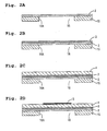
- Each of the upper electrodes 5 is provided on the surface of the piezoelectric layer 4 at an area corresponding to an opening 16a (see Figs. 2A to 2D) of one of the pressure chambers 16.
- Each of the upper electrodes 5 is connected to the drive circuit IC and used as a drive electrode.
- a predetermined drive signal is outputted from the drive circuit IC to a certain upper electrode 5 of the upper electrodes 5, then electric potential of the upper electrode 5 becomes higher than an electric potential of the lower electrode 3, and an electric field is applied in a polarization direction (direction of thickness) of the piezoelectric layer 4. Then, an area of the piezoelectric layer 4 sandwiched between the upper electrode 5 and the lower electrode 3 is extended in the thickness direction and is contracted in a plane direction of the piezoelectric layer 4.
- the area of the piezoelectric layer 4 and an area of the vibration plate 2 which correspond to an opening 16A of a pressure chamber 16 associated with the upper electrode 5 is locally deformed (unimorph deformation) to project toward the pressure chamber 16. Therefore, the volume of the pressure chamber 16 is decreased, a pressure of the ink 20 in the pressure chamber 16 is increased, and the ink 20 is jetted from the ink-discharge nozzle 19. Thereafter, when the upper electrode 5 returns to an electric potential same as the electric potential of the lower electrode 3, the piezoelectric layer 4 and the vibration plate 2 restore to their original shape and the volume of the pressure chamber 16 returns to the original volume, thereby sucking the ink 20 from the manifold channel communicating with the ink tank.
- holes which are to become the nozzle channels 18, the pressure channels 17, and the pressure chambers 16 are formed by etching in the manifold plate 13, the channel plate 14, and the pressure chamber plate 15 respectively. These plates 13 to 15 are formed of stainless steel.
- the manifold plate 13, the channel plate 14, and the pressure chamber plate 15 are joined in a laminated state, thereby forming a substantial part of the channel unit 11 (step for forming channel-unit forming body) . Since the nozzle plate 12 is formed of a synthetic resin material, the nozzle plate 12 is melted when heated at the time of annealing treatment which will be described later. Therefore, the nozzle plate 12 is not joined at this time but will be joined after the annealing treatment.
- the vibration plate 2 formed of stainless steel is overlapped with the channel unit 11, while being positioned on the upper surface of the pressure chamber plate 15 in the channel unit 11, and joined to the pressure chamber plate 15 by thermo-compression bonding, thereby closing the pressure chambers 16 by the vibration plate 2 (vibration plate joining step).
- the lower electrode 3 which also serves as a diffusion-preventive layer is formed on the vibration plate 2 (first electrode layer forming step).
- a paste is prepared in which silver nano-particles having a particle size of not more than 50 nm (in this embodiment, silver nano-particles having an average particle size of 50 nm) are dispersed in a dispersing agent, and then the paste is coated on the vibration plate 2.
- the metal-nano particles having a particle size of not more than 50 nm is a low-melting point material which is melted and fused at a temperature which is lower than an original melting point of the metal of the metal-nano particles.
- the calcination at a low temperature (sintering-start temperature) which is about 250°C to 420°C (in particular, 150°C to 400°C).
- a low temperature sining-start temperature
- the pre-calcination is performed at a minimum temperature and for a minimum duration of time because the calcination of the lower electrode 3 is advanced also in the annealing step which will be explained later.
- the effect of thermal history can be made as small as possible.
- the sintering-start temperature is sufficiently lower than the maximum shrink temperature as will be explained later, the calcination at the sintering-start temperature causes the conductive material forming the lower electrode 3 to become compact, but does not cause any growth and/or increase of grain boundary. Accordingly, it is possible to prevent the element contained in the vibration plate from diffusing in the piezoelectric layer.
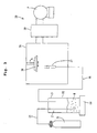
- FIG. 3 shows a schematic diagram of a film forming apparatus 30 for forming the piezoelectric layer 4.
- This film forming apparatus 30 includes an aerosol generator 31 which forms an aerosol Z by dispersing material particles M in a carrier gas, and a film forming chamber 35 for depositing aerosol Z on a substrate by jetting the aerosol Z from an ejection nozzle 37.
- the aerosol generator 31 includes an aerosol chamber 32 capable of accommodating the material particles M inside thereof, and a vibration unit 33 which is attached to the aerosol chamber 32 and which causes the aerosol chamber 32 to vibrate.
- a gas cylinder B for introducing the carrier gas is connected to the aerosol chamber 32 via an introduction pipe 34.
- An end of the introduction pipe 34 is positioned near the bottom surface in the aerosol chamber 32 so that the end is buried in the material particles M.
- an inert gas such as helium, argon, and nitrogen, or a gas such as air and oxygen can be used.
- the film forming chamber 35 includes a stage 36 for attaching or mounting the substrate where the piezoelectric layer 4 will be formed, and the ejection nozzle 37 which is provided below the stage 36.
- the ejection nozzle 37 is connected to the aerosol chamber 32 via an aerosol supply pipe 38 so as to supply the aerosol Z in the aerosol chamber 32 to the ejection nozzle 37 through the aerosol supply pipe 38.
- a vacuum pump P is connected to this film forming chamber 35 via a powder recovery unit 39 so as to decompress the inside of the film forming chamber 35.
- the vibration plate 2 is set in the stage 36.
- the material particles M are charged into the aerosol chamber 32.
- the material particles M for example, lead zirconate titanate (PZT) can be used.
- the carrier gas is introduced from the gas cylinder B so that the material particles M are made to rise up by gas pressure.
- the aerosol chamber 32 is vibrated by the vibration unit 33, thereby mixing the material particles M with the carrier gas to generate the aerosol Z.
- the inside of the film forming chamber 35 is decompressed by the vacuum pump P to generate pressure difference between the aerosol chamber 32 and the film forming chamber 35. Due to the pressure difference, the aerosol Z in the aerosol chamber 32 is ejected from the ejection nozzle 37 while accelerating the aerosol to a high velocity.
- the material particles M contained in the ejected aerosol Z are collided on the vibration plate 2 and deposited on the vibration plate 2, thereby forming the piezoelectric layer 4.
- the aerosol deposition method utilizes a phenomenon in which the material particles are completely solidified due the impact of collision
- the aerosol deposition method is a thin film formation process which does not require any calcination. By employing such a process for forming the piezoelectric layer, it is possible to minimize the thermal cycle during the production process.
- the annealing treatment is performed on the formed piezoelectric layer 4 (annealing treatment step).
- the annealing temperature can be 600°C to 1, 000°C, preferably 600°C to 900°C.
- the annealing treatment is performed at 900°C for 30 minutes. Since the sintering-start temperature of the lower electrode 3 is lower than this annealing temperature, the calcination of the lower electrode 3 is advanced by the annealing treatment. Accordingly, the lower electrode 3 adheres tightly to the vibration plate 2 and/or the piezoelectric layer 4.
- the annealing step required after the formation of piezoelectric layer 4 can also serve as a main calcination step for the lower electrode 3, the thermal cycle during the production process can be made as minimum as necessary, and the production process can be simplified.
- the piezoelectric layer 4 is formed by the aerosol deposition method, the crystallinity of the piezoelectric layer is different from that in a case when the piezoelectric layer is formed by a different method, such as a method of calcinating green sheet and the sputtering method. Accordingly, it is relatively easy to identify that the piezoelectric layer has been formed by the aerosol deposition method by analyzing the crystallinity with the X-ray diffraction or the like.
- Fig. 6 shows XRD (X-ray diffraction) spectra of a piezoelectric layer (sintered body) formed by calcinating green sheet and of a piezoelectric layer formed by the aerosol deposition method. From Fig. 6, it is appreciated that the spectrum of the piezoelectric sheet formed by the aerosol deposition method clearly has peaks at diffraction angles of about 45 degrees and about 55 degrees. On the other hand, the spectrum of the piezoelectric sheet formed by calcinating green sheet does not have peaks at the diffraction angles of these degrees. This indicates that the piezoelectric layer formed by calcinating green sheet and the piezoelectric layer formed by the aerosol deposition method have mutually different crystalline structures.
- XRD X-ray diffraction
- the sintering-start temperature of the lower electrode 3 will be explained.
- the term "sintering-start temperature" in the present application means a temperature (shrinkage-start temperature) at which a conductive material starts to shrink due to the heating during calcination of the conductive material.
- Fig. 4 shows a change in a shrinkage coefficient of conductive materials containing Ag particles having different average particle sizes respectively, with respect to temperature (behavior of the conductive materials during calcination).
- the shrinkage coefficient was calculated from a measured value of stress exerted on the electrode layer measured with a stress measurement device. Any of the conductive materials starts to shrink at a predetermined temperature as being heated.
- the shrinkage of a conductive material is caused by a melting of metal particles contained in the conductive material.
- the shrinkage-start temperature is a temperature at which the shrinkage coefficient starts to increase from 0% (to increase in the negative direction). From Fig. 4, it is appreciated that the shrinkage-start temperature is different depending on the particle size of Ag particles contained in the conductive material. When the particle size is 10 nm (0.01 ⁇ m), the shrinkage-start temperature is about 150°C; and a gap between the metal particles disappears as the metal particles are melted as the temperature is elevated (heating), and the shrinkage coefficient is increased. Then, the shrinkage coefficient reaches a maximum value at around 270°C (maximum shrink temperature). Afterwards, as the temperature is further elevated beyond this temperature, the shrinkage coefficient is gradually decreased.
- the grain boundary (border) in the conductive material is substantially great and is developed, for example, to an extent surpassing 1 ⁇ m. It is conceived that when the grain boundary (boarder) is developed in this manner, the element forming the substrate is easily diffused in the piezoelectric layer. Therefore, in view of preventing the diffusion, the annealing temperature preferably does not exceed the maximum shrink temperature.
- the shrinkage-start temperature is about 200°C, and the shrinkage coefficient is increased as the temperature is elevated. Then, the shrinkage coefficient reaches a maximum value at around 400°C (maximum shrink temperature). Afterwards, as the temperature is further elevated beyond this temperature, the shrinkage coefficient is gradually decreased.
- the particle size is 700 nm (0.7 ⁇ m)
- the shrinkage-start temperature is about 330°C
- the maximum shrink temperature is 700°C.
- the particle size is 1,200 nm (1.2 ⁇ m)
- the shrinkage-start temperature is about 420°C
- the maximum shrink temperature is 800°C. From Fig. 5 showing a change in the maximum shrink temperature with respect to the average particle size, it is appreciated that the particle size is preferably small in a relationship between the particle size and the annealing temperature because the maximum shrink temperature is increased depending on the particle size.
- the shrinkage coefficient of the average particle size of 50 nm and 10 nm was calculated as follows by using a paste including commercially available silver particles (particle size: 5 nm). A logarithmic indication of the maximum shrink temperature with respect to the various average particle sizes is expected to be substantially linear.
- R 2 is also called as a coefficient of determination, and is an index which is commonly used as a value showing a statistical certainty.
- the coefficient of determination is an amount of statistic expressing a proportion of a portion where a variation of Y can be explained by a variation of X when a variable Y (explained variable) is subjected to regression analysis by a certain variable X (explanatory variable).
- the coefficient of determination takes a value between 0 and 1 (it shows that as the coefficient of determination is closer to 1, the proportion of the portion which can be explained is higher)
- temperatures at which the particle size of 10 nm and 50 nm attain the maximum shrinkage coefficient (maximum shrink temperature) respectively were estimated, and temperature of 270°C for 10 nm and temperature of 400°C for 50 nm were calculated.
- the upper electrodes 5 and a plurality of lead portions (not shown in the diagram) connected to the upper electrodes 5 respectively are formed at areas on the upper surface of piezoelectric layer 4, each of the areas corresponding to one of the pressure chambers 16 (second electrode forming step).
- a predetermined pattern may be formed by using a photolithographic etching method, or may be formed by screen printing directly on the upper surface of the piezoelectric layer 4.
- a metal-nano particles which can start to sinter at a low temperature is used as a conductive material for forming the lower electrode 3 on the vibration plate 2.
- the piezoelectric layer 4 is formed by using the aerosol deposition method (a method forming a thin film by blowing aerosol containing material particles onto a target object to deposit the material particles thereon) which requires no calcination step. According to such a process, in either of the steps for forming lower electrode and for forming piezoelectric layer, there is no need to perform calcination under a severe condition (elevated temperature).
- the calcination of the lower electrode 3 can be advanced also at the same time. Accordingly, the thermal cycle during the production process can be suppressed as minimum as necessary, thereby suppressing the exfoliation of layers and the diffusion of material forming the vibration plate 2 into the piezoelectric layer due to the thermal history. Thus, it is possible to lower the degradation of piezoelectric characteristics. Further, it is possible to simplify the producing process.
Landscapes
- Engineering & Computer Science (AREA)
- Manufacturing & Machinery (AREA)
- Particle Formation And Scattering Control In Inkjet Printers (AREA)
Applications Claiming Priority (1)
| Application Number | Priority Date | Filing Date | Title |
|---|---|---|---|
| JP2005082285 | 2005-03-22 |
Publications (3)
| Publication Number | Publication Date |
|---|---|
| EP1705016A2 true EP1705016A2 (fr) | 2006-09-27 |
| EP1705016A3 EP1705016A3 (fr) | 2007-09-05 |
| EP1705016B1 EP1705016B1 (fr) | 2011-04-27 |
Family
ID=36577491
Family Applications (1)
| Application Number | Title | Priority Date | Filing Date |
|---|---|---|---|
| EP06005758A Expired - Lifetime EP1705016B1 (fr) | 2005-03-22 | 2006-03-21 | Actuateur piézo-électrique, tête à jet d'encre, méthode de production d'un actuateur piézo-électrique et méthode de production d'une tête à jet d'encre |
Country Status (4)
| Country | Link |
|---|---|
| US (2) | US20060255692A1 (fr) |
| EP (1) | EP1705016B1 (fr) |
| AT (1) | ATE507076T1 (fr) |
| DE (1) | DE602006021500D1 (fr) |
Cited By (2)
| Publication number | Priority date | Publication date | Assignee | Title |
|---|---|---|---|---|
| WO2013011217A1 (fr) * | 2011-07-18 | 2013-01-24 | Renault Sas | Procédé d'assemblage d'un transducteur ultrasonore et transducteur obtenu par le procédé |
| WO2019122402A1 (fr) * | 2017-12-22 | 2019-06-27 | Luxembourg Institute Of Science And Technology (List) | Dispositif piézoélectrique pourvu d'un capteur et procédé destiné à mesurer le comportement dudit dispositif piézoélectrique |
Families Citing this family (2)
| Publication number | Priority date | Publication date | Assignee | Title |
|---|---|---|---|---|
| IT202000010264A1 (it) * | 2020-05-07 | 2021-11-07 | St Microelectronics Srl | Attuatore piezoelettrico avente un sensore di deformazione e relativo procedimento di fabbricazione |
| IT202000010261A1 (it) | 2020-05-07 | 2021-11-07 | St Microelectronics Srl | Attuatore piezoelettrico dotato di una struttura deformabile avente migliorate proprieta' meccaniche e relativo procedimento di fabbricazione |
Citations (3)
| Publication number | Priority date | Publication date | Assignee | Title |
|---|---|---|---|---|
| JPH11334087A (ja) | 1998-05-27 | 1999-12-07 | Mita Ind Co Ltd | インクジェットヘッドの製造方法 |
| EP1500509A1 (fr) | 2003-07-15 | 2005-01-26 | Brother Kogyo Kabushiki Kaisha | Dispositif de distribution de liquide et sa méthode de fabrication |
| EP1693907A1 (fr) | 2005-02-21 | 2006-08-23 | Brother Kogyo Kabushiki Kaisha | Actionneur piézoélectrique et son procédé de fabrication |
Family Cites Families (8)
| Publication number | Priority date | Publication date | Assignee | Title |
|---|---|---|---|---|
| DE3004080C2 (de) * | 1980-02-05 | 1986-03-20 | Sigri GmbH, 8901 Meitingen | Verfahren zum Beschichten einer porösen Elektrode |
| JPS60159185A (ja) * | 1984-01-31 | 1985-08-20 | Permelec Electrode Ltd | 電極の製造方法 |
| JPS62277780A (ja) * | 1986-05-26 | 1987-12-02 | Matsushita Electric Works Ltd | 圧電セラミツクス体の製法 |
| JPS63112499A (ja) * | 1986-10-31 | 1988-05-17 | Nippon Telegr & Teleph Corp <Ntt> | リチウムテトラボレ−ト圧電性薄膜の形成法 |
| DE69600167T2 (de) * | 1995-04-03 | 1998-10-22 | Seiko Epson Corp | Tintenstrahldruckkopf und dessen Herstellungsverfahren |
| US6531187B2 (en) * | 1999-04-23 | 2003-03-11 | Agency Of Industrial Science And Technology | Method of forming a shaped body of brittle ultra fine particles with mechanical impact force and without heating |
| US6740900B2 (en) * | 2002-02-27 | 2004-05-25 | Konica Corporation | Organic thin-film transistor and manufacturing method for the same |
| JP3879685B2 (ja) * | 2002-03-18 | 2007-02-14 | セイコーエプソン株式会社 | 圧電素子、圧電アクチュエータ、及び、液体噴射ヘッド |
-
2006
- 2006-03-20 US US11/276,999 patent/US20060255692A1/en not_active Abandoned
- 2006-03-21 DE DE602006021500T patent/DE602006021500D1/de not_active Expired - Lifetime
- 2006-03-21 AT AT06005758T patent/ATE507076T1/de not_active IP Right Cessation
- 2006-03-21 EP EP06005758A patent/EP1705016B1/fr not_active Expired - Lifetime
- 2006-09-12 US US11/531,269 patent/US7685686B2/en not_active Expired - Fee Related
Patent Citations (3)
| Publication number | Priority date | Publication date | Assignee | Title |
|---|---|---|---|---|
| JPH11334087A (ja) | 1998-05-27 | 1999-12-07 | Mita Ind Co Ltd | インクジェットヘッドの製造方法 |
| EP1500509A1 (fr) | 2003-07-15 | 2005-01-26 | Brother Kogyo Kabushiki Kaisha | Dispositif de distribution de liquide et sa méthode de fabrication |
| EP1693907A1 (fr) | 2005-02-21 | 2006-08-23 | Brother Kogyo Kabushiki Kaisha | Actionneur piézoélectrique et son procédé de fabrication |
Cited By (5)
| Publication number | Priority date | Publication date | Assignee | Title |
|---|---|---|---|---|
| WO2013011217A1 (fr) * | 2011-07-18 | 2013-01-24 | Renault Sas | Procédé d'assemblage d'un transducteur ultrasonore et transducteur obtenu par le procédé |
| FR2978301A1 (fr) * | 2011-07-18 | 2013-01-25 | Renault Sa | Procede d'assemblage d'un transducteur ultrasonore et transducteur obtenu par le procede |
| US9780288B2 (en) | 2011-07-18 | 2017-10-03 | Renault S.A.S. | Method of assembling an ultrasonic transducer and the transducer obtained thereby |
| WO2019122402A1 (fr) * | 2017-12-22 | 2019-06-27 | Luxembourg Institute Of Science And Technology (List) | Dispositif piézoélectrique pourvu d'un capteur et procédé destiné à mesurer le comportement dudit dispositif piézoélectrique |
| LU100594B1 (en) * | 2017-12-22 | 2019-06-28 | Luxembourg Inst Science & Tech List | Piezoelectric device with a sensor and method for measuring the behaviour of said peizoelectric device |
Also Published As
| Publication number | Publication date |
|---|---|
| US7685686B2 (en) | 2010-03-30 |
| US20060255692A1 (en) | 2006-11-16 |
| EP1705016A3 (fr) | 2007-09-05 |
| EP1705016B1 (fr) | 2011-04-27 |
| US20070052765A1 (en) | 2007-03-08 |
| ATE507076T1 (de) | 2011-05-15 |
| DE602006021500D1 (de) | 2011-06-09 |
Similar Documents
| Publication | Publication Date | Title |
|---|---|---|
| JP4386924B2 (ja) | インクジェットヘッドの圧電アクチュエータの形成方法 | |
| US20060207078A1 (en) | Laminate-type piezoelectric device and method for manufacturing the same | |
| CN2736166Y (zh) | 液体输送装置 | |
| EP1705016B1 (fr) | Actuateur piézo-électrique, tête à jet d'encre, méthode de production d'un actuateur piézo-électrique et méthode de production d'une tête à jet d'encre | |
| EP1693907B1 (fr) | Procédé de fabrication d'un actionneur piézoélectrique | |
| JP2004096068A (ja) | 圧電素子、圧電アクチュエータ、及び、液体噴射ヘッド | |
| JP2006297915A (ja) | 圧電アクチュエータ、インクジェットヘッドおよびそれらの製造方法 | |
| CN1976197B (zh) | 压电促动器、检查方法和液体喷射设备 | |
| TWI546199B (zh) | 壓電致動器及其製造方法 | |
| JP2006093348A (ja) | 圧電アクチュエータおよびインクジェットヘッドの製造方法 | |
| JP3975979B2 (ja) | 液体移送装置の製造方法 | |
| US7771780B2 (en) | Method of producing composite material, method of producing piezoelectric actuator, method of producing ink-jet head, and piezoelectric actuator | |
| JP2001156351A (ja) | 積層構造電極、その形成方法、及び圧電アクチュエータ | |
| JP2006261656A (ja) | 圧電アクチュエータおよびその製造方法 | |
| JP5043311B2 (ja) | 圧電積層体及びその製造方法,圧電スピーカ,電子機器 | |
| JP2006229154A (ja) | 圧電アクチュエータ、インクジェットヘッド、およびそれらの製造方法 | |
| JP3340043B2 (ja) | 圧電アクチュエータとその製造方法 | |
| JP2003309301A (ja) | デバイス製造方法 | |
| JP2001047623A (ja) | インクジェットプリンターヘッド | |
| JP2006054442A (ja) | 圧電アクチュエータ及びインクジェットヘッドの製造方法、圧電アクチュエータ及びインクジェットヘッド | |
| US20030168784A1 (en) | Method of fabricating a ceramic stack structure | |
| JP2007268838A (ja) | インクジェットヘッド | |
| EP1757714A2 (fr) | Méthode de production d'un film et d'une tête à jet d'encre | |
| JP4276862B2 (ja) | 圧電アクチュエータおよびインクジェット記録ヘッド | |
| JP2005353746A (ja) | アクチュエータ及びインクジェットヘッド |
Legal Events
| Date | Code | Title | Description |
|---|---|---|---|
| PUAI | Public reference made under article 153(3) epc to a published international application that has entered the european phase |
Free format text: ORIGINAL CODE: 0009012 |
|
| AK | Designated contracting states |
Kind code of ref document: A2 Designated state(s): AT BE BG CH CY CZ DE DK EE ES FI FR GB GR HU IE IS IT LI LT LU LV MC NL PL PT RO SE SI SK TR |
|
| AX | Request for extension of the european patent |
Extension state: AL BA HR MK YU |
|
| PUAL | Search report despatched |
Free format text: ORIGINAL CODE: 0009013 |
|
| AK | Designated contracting states |
Kind code of ref document: A3 Designated state(s): AT BE BG CH CY CZ DE DK EE ES FI FR GB GR HU IE IS IT LI LT LU LV MC NL PL PT RO SE SI SK TR |
|
| AX | Request for extension of the european patent |
Extension state: AL BA HR MK YU |
|
| 17P | Request for examination filed |
Effective date: 20080304 |
|
| AKX | Designation fees paid |
Designated state(s): AT BE BG CH CY CZ DE DK EE ES FI FR GB GR HU IE IS IT LI LT LU LV MC NL PL PT RO SE SI SK TR |
|
| 17Q | First examination report despatched |
Effective date: 20080929 |
|
| GRAP | Despatch of communication of intention to grant a patent |
Free format text: ORIGINAL CODE: EPIDOSNIGR1 |
|
| GRAS | Grant fee paid |
Free format text: ORIGINAL CODE: EPIDOSNIGR3 |
|
| GRAA | (expected) grant |
Free format text: ORIGINAL CODE: 0009210 |
|
| AK | Designated contracting states |
Kind code of ref document: B1 Designated state(s): AT BE BG CH CY CZ DE DK EE ES FI FR GB GR HU IE IS IT LI LT LU LV MC NL PL PT RO SE SI SK TR |
|
| REG | Reference to a national code |
Ref country code: GB Ref legal event code: FG4D |
|
| REG | Reference to a national code |
Ref country code: CH Ref legal event code: EP |
|
| REG | Reference to a national code |
Ref country code: IE Ref legal event code: FG4D |
|
| REF | Corresponds to: |
Ref document number: 602006021500 Country of ref document: DE Date of ref document: 20110609 Kind code of ref document: P |
|
| REG | Reference to a national code |
Ref country code: DE Ref legal event code: R096 Ref document number: 602006021500 Country of ref document: DE Effective date: 20110609 |
|
| REG | Reference to a national code |
Ref country code: NL Ref legal event code: VDEP Effective date: 20110427 |
|
| LTIE | Lt: invalidation of european patent or patent extension |
Effective date: 20110427 |
|
| PG25 | Lapsed in a contracting state [announced via postgrant information from national office to epo] |
Ref country code: PT Free format text: LAPSE BECAUSE OF FAILURE TO SUBMIT A TRANSLATION OF THE DESCRIPTION OR TO PAY THE FEE WITHIN THE PRESCRIBED TIME-LIMIT Effective date: 20110829 Ref country code: LT Free format text: LAPSE BECAUSE OF FAILURE TO SUBMIT A TRANSLATION OF THE DESCRIPTION OR TO PAY THE FEE WITHIN THE PRESCRIBED TIME-LIMIT Effective date: 20110427 Ref country code: SE Free format text: LAPSE BECAUSE OF FAILURE TO SUBMIT A TRANSLATION OF THE DESCRIPTION OR TO PAY THE FEE WITHIN THE PRESCRIBED TIME-LIMIT Effective date: 20110427 |
|
| PG25 | Lapsed in a contracting state [announced via postgrant information from national office to epo] |
Ref country code: BE Free format text: LAPSE BECAUSE OF FAILURE TO SUBMIT A TRANSLATION OF THE DESCRIPTION OR TO PAY THE FEE WITHIN THE PRESCRIBED TIME-LIMIT Effective date: 20110427 Ref country code: CY Free format text: LAPSE BECAUSE OF FAILURE TO SUBMIT A TRANSLATION OF THE DESCRIPTION OR TO PAY THE FEE WITHIN THE PRESCRIBED TIME-LIMIT Effective date: 20110427 Ref country code: SI Free format text: LAPSE BECAUSE OF FAILURE TO SUBMIT A TRANSLATION OF THE DESCRIPTION OR TO PAY THE FEE WITHIN THE PRESCRIBED TIME-LIMIT Effective date: 20110427 Ref country code: ES Free format text: LAPSE BECAUSE OF FAILURE TO SUBMIT A TRANSLATION OF THE DESCRIPTION OR TO PAY THE FEE WITHIN THE PRESCRIBED TIME-LIMIT Effective date: 20110807 Ref country code: IS Free format text: LAPSE BECAUSE OF FAILURE TO SUBMIT A TRANSLATION OF THE DESCRIPTION OR TO PAY THE FEE WITHIN THE PRESCRIBED TIME-LIMIT Effective date: 20110827 Ref country code: AT Free format text: LAPSE BECAUSE OF FAILURE TO SUBMIT A TRANSLATION OF THE DESCRIPTION OR TO PAY THE FEE WITHIN THE PRESCRIBED TIME-LIMIT Effective date: 20110427 Ref country code: FI Free format text: LAPSE BECAUSE OF FAILURE TO SUBMIT A TRANSLATION OF THE DESCRIPTION OR TO PAY THE FEE WITHIN THE PRESCRIBED TIME-LIMIT Effective date: 20110427 Ref country code: LV Free format text: LAPSE BECAUSE OF FAILURE TO SUBMIT A TRANSLATION OF THE DESCRIPTION OR TO PAY THE FEE WITHIN THE PRESCRIBED TIME-LIMIT Effective date: 20110427 Ref country code: GR Free format text: LAPSE BECAUSE OF FAILURE TO SUBMIT A TRANSLATION OF THE DESCRIPTION OR TO PAY THE FEE WITHIN THE PRESCRIBED TIME-LIMIT Effective date: 20110728 |
|
| PG25 | Lapsed in a contracting state [announced via postgrant information from national office to epo] |
Ref country code: NL Free format text: LAPSE BECAUSE OF FAILURE TO SUBMIT A TRANSLATION OF THE DESCRIPTION OR TO PAY THE FEE WITHIN THE PRESCRIBED TIME-LIMIT Effective date: 20110427 |
|
| PG25 | Lapsed in a contracting state [announced via postgrant information from national office to epo] |
Ref country code: EE Free format text: LAPSE BECAUSE OF FAILURE TO SUBMIT A TRANSLATION OF THE DESCRIPTION OR TO PAY THE FEE WITHIN THE PRESCRIBED TIME-LIMIT Effective date: 20110427 Ref country code: CZ Free format text: LAPSE BECAUSE OF FAILURE TO SUBMIT A TRANSLATION OF THE DESCRIPTION OR TO PAY THE FEE WITHIN THE PRESCRIBED TIME-LIMIT Effective date: 20110427 |
|
| PG25 | Lapsed in a contracting state [announced via postgrant information from national office to epo] |
Ref country code: SK Free format text: LAPSE BECAUSE OF FAILURE TO SUBMIT A TRANSLATION OF THE DESCRIPTION OR TO PAY THE FEE WITHIN THE PRESCRIBED TIME-LIMIT Effective date: 20110427 Ref country code: RO Free format text: LAPSE BECAUSE OF FAILURE TO SUBMIT A TRANSLATION OF THE DESCRIPTION OR TO PAY THE FEE WITHIN THE PRESCRIBED TIME-LIMIT Effective date: 20110427 Ref country code: DK Free format text: LAPSE BECAUSE OF FAILURE TO SUBMIT A TRANSLATION OF THE DESCRIPTION OR TO PAY THE FEE WITHIN THE PRESCRIBED TIME-LIMIT Effective date: 20110427 Ref country code: PL Free format text: LAPSE BECAUSE OF FAILURE TO SUBMIT A TRANSLATION OF THE DESCRIPTION OR TO PAY THE FEE WITHIN THE PRESCRIBED TIME-LIMIT Effective date: 20110427 |
|
| PLBE | No opposition filed within time limit |
Free format text: ORIGINAL CODE: 0009261 |
|
| STAA | Information on the status of an ep patent application or granted ep patent |
Free format text: STATUS: NO OPPOSITION FILED WITHIN TIME LIMIT |
|
| 26N | No opposition filed |
Effective date: 20120130 |
|
| REG | Reference to a national code |
Ref country code: DE Ref legal event code: R097 Ref document number: 602006021500 Country of ref document: DE Effective date: 20120130 |
|
| PG25 | Lapsed in a contracting state [announced via postgrant information from national office to epo] |
Ref country code: IT Free format text: LAPSE BECAUSE OF FAILURE TO SUBMIT A TRANSLATION OF THE DESCRIPTION OR TO PAY THE FEE WITHIN THE PRESCRIBED TIME-LIMIT Effective date: 20110427 |
|
| PG25 | Lapsed in a contracting state [announced via postgrant information from national office to epo] |
Ref country code: MC Free format text: LAPSE BECAUSE OF NON-PAYMENT OF DUE FEES Effective date: 20120331 |
|
| REG | Reference to a national code |
Ref country code: CH Ref legal event code: PL |
|
| REG | Reference to a national code |
Ref country code: IE Ref legal event code: MM4A |
|
| PG25 | Lapsed in a contracting state [announced via postgrant information from national office to epo] |
Ref country code: IE Free format text: LAPSE BECAUSE OF NON-PAYMENT OF DUE FEES Effective date: 20120321 Ref country code: LI Free format text: LAPSE BECAUSE OF NON-PAYMENT OF DUE FEES Effective date: 20120331 Ref country code: CH Free format text: LAPSE BECAUSE OF NON-PAYMENT OF DUE FEES Effective date: 20120331 |
|
| PG25 | Lapsed in a contracting state [announced via postgrant information from national office to epo] |
Ref country code: BG Free format text: LAPSE BECAUSE OF FAILURE TO SUBMIT A TRANSLATION OF THE DESCRIPTION OR TO PAY THE FEE WITHIN THE PRESCRIBED TIME-LIMIT Effective date: 20110727 |
|
| PG25 | Lapsed in a contracting state [announced via postgrant information from national office to epo] |
Ref country code: TR Free format text: LAPSE BECAUSE OF FAILURE TO SUBMIT A TRANSLATION OF THE DESCRIPTION OR TO PAY THE FEE WITHIN THE PRESCRIBED TIME-LIMIT Effective date: 20110427 |
|
| PG25 | Lapsed in a contracting state [announced via postgrant information from national office to epo] |
Ref country code: LU Free format text: LAPSE BECAUSE OF NON-PAYMENT OF DUE FEES Effective date: 20120321 |
|
| PG25 | Lapsed in a contracting state [announced via postgrant information from national office to epo] |
Ref country code: HU Free format text: LAPSE BECAUSE OF FAILURE TO SUBMIT A TRANSLATION OF THE DESCRIPTION OR TO PAY THE FEE WITHIN THE PRESCRIBED TIME-LIMIT Effective date: 20060321 |
|
| REG | Reference to a national code |
Ref country code: FR Ref legal event code: PLFP Year of fee payment: 10 |
|
| PGFP | Annual fee paid to national office [announced via postgrant information from national office to epo] |
Ref country code: FR Payment date: 20150224 Year of fee payment: 10 Ref country code: GB Payment date: 20150224 Year of fee payment: 10 |
|
| PGFP | Annual fee paid to national office [announced via postgrant information from national office to epo] |
Ref country code: DE Payment date: 20150331 Year of fee payment: 10 |
|
| REG | Reference to a national code |
Ref country code: DE Ref legal event code: R119 Ref document number: 602006021500 Country of ref document: DE |
|
| GBPC | Gb: european patent ceased through non-payment of renewal fee |
Effective date: 20160321 |
|
| REG | Reference to a national code |
Ref country code: FR Ref legal event code: ST Effective date: 20161130 |
|
| PG25 | Lapsed in a contracting state [announced via postgrant information from national office to epo] |
Ref country code: DE Free format text: LAPSE BECAUSE OF NON-PAYMENT OF DUE FEES Effective date: 20161001 Ref country code: FR Free format text: LAPSE BECAUSE OF NON-PAYMENT OF DUE FEES Effective date: 20160331 Ref country code: GB Free format text: LAPSE BECAUSE OF NON-PAYMENT OF DUE FEES Effective date: 20160321 |