EP1705681B1 - Panneau d'affichage à plasma et son procédé de fabrication - Google Patents
Panneau d'affichage à plasma et son procédé de fabrication Download PDFInfo
- Publication number
- EP1705681B1 EP1705681B1 EP05112475A EP05112475A EP1705681B1 EP 1705681 B1 EP1705681 B1 EP 1705681B1 EP 05112475 A EP05112475 A EP 05112475A EP 05112475 A EP05112475 A EP 05112475A EP 1705681 B1 EP1705681 B1 EP 1705681B1
- Authority
- EP
- European Patent Office
- Prior art keywords
- dielectric layer
- electrode
- layer
- photosensitive material
- discharge space
- Prior art date
- Legal status (The legal status is an assumption and is not a legal conclusion. Google has not performed a legal analysis and makes no representation as to the accuracy of the status listed.)
- Expired - Lifetime
Links
Images




Classifications
-
- B—PERFORMING OPERATIONS; TRANSPORTING
- B62—LAND VEHICLES FOR TRAVELLING OTHERWISE THAN ON RAILS
- B62J—CYCLE SADDLES OR SEATS; AUXILIARY DEVICES OR ACCESSORIES SPECIALLY ADAPTED TO CYCLES AND NOT OTHERWISE PROVIDED FOR, e.g. ARTICLE CARRIERS OR CYCLE PROTECTORS
- B62J99/00—Subject matter not provided for in other groups of this subclass
-
- H—ELECTRICITY
- H01—ELECTRIC ELEMENTS
- H01J—ELECTRIC DISCHARGE TUBES OR DISCHARGE LAMPS
- H01J11/00—Gas-filled discharge tubes with alternating current induction of the discharge, e.g. alternating current plasma display panels [AC-PDP]; Gas-filled discharge tubes without any main electrode inside the vessel; Gas-filled discharge tubes with at least one main electrode outside the vessel
- H01J11/20—Constructional details
- H01J11/34—Vessels, containers or parts thereof, e.g. substrates
- H01J11/40—Layers for protecting or enhancing the electron emission, e.g. MgO layers
-
- B—PERFORMING OPERATIONS; TRANSPORTING
- B62—LAND VEHICLES FOR TRAVELLING OTHERWISE THAN ON RAILS
- B62J—CYCLE SADDLES OR SEATS; AUXILIARY DEVICES OR ACCESSORIES SPECIALLY ADAPTED TO CYCLES AND NOT OTHERWISE PROVIDED FOR, e.g. ARTICLE CARRIERS OR CYCLE PROTECTORS
- B62J27/00—Safety equipment
-
- H—ELECTRICITY
- H01—ELECTRIC ELEMENTS
- H01J—ELECTRIC DISCHARGE TUBES OR DISCHARGE LAMPS
- H01J11/00—Gas-filled discharge tubes with alternating current induction of the discharge, e.g. alternating current plasma display panels [AC-PDP]; Gas-filled discharge tubes without any main electrode inside the vessel; Gas-filled discharge tubes with at least one main electrode outside the vessel
- H01J11/10—AC-PDPs with at least one main electrode being out of contact with the plasma
- H01J11/16—AC-PDPs with at least one main electrode being out of contact with the plasma with main electrodes provided inside or on the side face of the spacers
-
- H—ELECTRICITY
- H01—ELECTRIC ELEMENTS
- H01J—ELECTRIC DISCHARGE TUBES OR DISCHARGE LAMPS
- H01J11/00—Gas-filled discharge tubes with alternating current induction of the discharge, e.g. alternating current plasma display panels [AC-PDP]; Gas-filled discharge tubes without any main electrode inside the vessel; Gas-filled discharge tubes with at least one main electrode outside the vessel
- H01J11/20—Constructional details
- H01J11/22—Electrodes, e.g. special shape, material or configuration
- H01J11/24—Sustain electrodes or scan electrodes
-
- H—ELECTRICITY
- H01—ELECTRIC ELEMENTS
- H01J—ELECTRIC DISCHARGE TUBES OR DISCHARGE LAMPS
- H01J11/00—Gas-filled discharge tubes with alternating current induction of the discharge, e.g. alternating current plasma display panels [AC-PDP]; Gas-filled discharge tubes without any main electrode inside the vessel; Gas-filled discharge tubes with at least one main electrode outside the vessel
- H01J11/20—Constructional details
- H01J11/34—Vessels, containers or parts thereof, e.g. substrates
- H01J11/36—Spacers, barriers, ribs, partitions or the like
-
- H—ELECTRICITY
- H01—ELECTRIC ELEMENTS
- H01J—ELECTRIC DISCHARGE TUBES OR DISCHARGE LAMPS
- H01J9/00—Apparatus or processes specially adapted for the manufacture, installation, removal, maintenance of electric discharge tubes, discharge lamps, or parts thereof; Recovery of material from discharge tubes or lamps
- H01J9/02—Manufacture of electrodes or electrode systems
-
- H—ELECTRICITY
- H01—ELECTRIC ELEMENTS
- H01J—ELECTRIC DISCHARGE TUBES OR DISCHARGE LAMPS
- H01J9/00—Apparatus or processes specially adapted for the manufacture, installation, removal, maintenance of electric discharge tubes, discharge lamps, or parts thereof; Recovery of material from discharge tubes or lamps
- H01J9/24—Manufacture or joining of vessels, leading-in conductors or bases
- H01J9/241—Manufacture or joining of vessels, leading-in conductors or bases the vessel being for a flat panel display
- H01J9/242—Spacers between faceplate and backplate
-
- A—HUMAN NECESSITIES
- A61—MEDICAL OR VETERINARY SCIENCE; HYGIENE
- A61H—PHYSICAL THERAPY APPARATUS, e.g. DEVICES FOR LOCATING OR STIMULATING REFLEX POINTS IN THE BODY; ARTIFICIAL RESPIRATION; MASSAGE; BATHING DEVICES FOR SPECIAL THERAPEUTIC OR HYGIENIC PURPOSES OR SPECIFIC PARTS OF THE BODY
- A61H23/00—Percussion or vibration massage, e.g. using supersonic vibration; Suction-vibration massage; Massage with moving diaphragms
- A61H23/004—With mechanical drive, e.g. spring mechanism or vibrating unit being hit for starting vibration and then applied to the body of a patient
-
- H—ELECTRICITY
- H01—ELECTRIC ELEMENTS
- H01J—ELECTRIC DISCHARGE TUBES OR DISCHARGE LAMPS
- H01J2211/00—Plasma display panels with alternate current induction of the discharge, e.g. AC-PDPs
- H01J2211/20—Constructional details
- H01J2211/22—Electrodes
- H01J2211/24—Sustain electrodes or scan electrodes
- H01J2211/245—Shape, e.g. cross section or pattern
Definitions
- the present invention relates to a plasma display panel (PDP) having an opposing discharge structure. More particularly, the present invention relates to a PDP that may be easily formed, has high light transmittance and luminescence efficiency, and a manufacturing method thereof.
- PDP plasma display panel
- a rear substrate and a front substrate are assembled facing each other, an inert gas is filled in a discharge space between the rear substrate and the front substrate, and glow discharge is generated in the discharge space.
- the rear substrate is provided by forming an address electrode on a rear substrate, covering the address electrode with a dielectric layer, forming a barrier rib on the dielectric layer and forming a phosphor layer within the areas bounded by the barrier rib.
- the front substrate facing the rear substrate is provided by forming an electrode pair having a sustain electrode and a scan electrode on a front substrate, the electrode pair being orthogonal to the address electrode, and covering the electrode pair with a stacked structure including a dielectric layer and a protective layer.
- the PDP generates plasma from the glow discharge in the discharge space.
- Vacuum ultraviolet (VUV) rays are generated by the plasma, and the phosphor is excited by the VUV rays. Subsequently an image is displayed using red, green and blue light generated by the phosphor.
- VUV Vacuum ultraviolet
- the sustain electrodes and the scan electrodes formed on the front substrate of the PDP are typically opaque. Accordingly, visible light emitted by the phosphor is blocked by the sustain electrodes and the scan electrodes, decreasing light transmittance.
- a PDP has a surface discharge structure, high voltage is required and luminescence efficiency is low during sustain discharge. In order to overcome these problems, a PDP having an opposing discharge structure is required, as the following operational explanation illustrates.
- Glow discharge is generated by applying a voltage, higher than discharge firing voltage, between two electrodes. Once the discharge is generated, voltage distribution between a cathode and an anode has a distorted form due to a space charge effect generated on the dielectric layer in the periphery of the cathode and the anode. That is, regions of a cathode sheath, an anode sheath, and a positive column are formed between the two electrodes. Most of the voltage applied to the two electrodes for the discharge is consumed in the cathode sheath region in the periphery of the cathode. A portion of the voltage is consumed in the anode sheath region in the periphery of the anode. The positive column region is formed between the cathode sheath region and the anode sheath region, and consumes negligible voltage.
- a PDP having an opposing discharge structure increases a positive column generated between an anode sheath and a cathode sheath during glow discharge, thus improving luminescence efficiency compared to a PDP having a surface discharge structure.
- United States Patent Application Publication No. 2004/0245929 A1 discloses a gas-discharge display device comprising, one upon the other, address electrodes, an undercoat, partition walls, first and second electrodes, and a dielectric cover layer, as well as a discharge space whose bottom is defined by the undercoat and whose sidewalls are defined by the partition walls and the dielectric cover layer, and a phosphor layer in the discharge space.
- the present invention is directed to a plasma display panel (PDP) and a manufacturing method thereof, which substantially overcome one or more of the problems due to the limitations and disadvantages of the prior art.
- PDP plasma display panel
- a PDP including a first substrate, an address electrode formed on the first substrate and extending in a first direction, a first dielectric layer covering the address electrode, a second dielectric layer on the first dielectric layer, a first electrode and a second electrode alternately disposed on the second dielectric layer and extending in a second direction, a third dielectric layer covering the first electrode and the second electrode, a discharge space, the discharge space having a bottom defined by the first dielectric layer at a bottom of the discharge space and sidewalls defined by the second and third dielectric layers, a phosphor layer in the discharge space and a first photosensitive material layer between the first dielectric layer and the second dielectric layer.
- the second direction may be orthogonal to the first direction and the first photosensitive material layer may be where the second dielectric layer intersects the address electrode.
- a width of the first photosensitive material layer may be substantially coextensive with a width of the second dielectric layer, the widths being measured in the first direction.
- the second dielectric layer may include a first member disposed between adjacent address electrodes and extending in the first direction and a second member orthogonal to and crossing the address electrode.
- the third dielectric layer may include a third member corresponding to the first member and a fourth member crossing the third member and corresponding to the second member.
- the third dielectric layer may have a protective layer formed thereon inside the discharge space.
- the protective layer may be opaque.
- the second dielectric layer and the third dielectric layer may be formed of a same dielectric material.
- the address electrode, the first electrode, and the second electrode may be formed of a conductive, opaque material. In a cross-section of the first electrode and the second electrode, a dimension in a horizontal direction of the first electrode and the second electrode may be less than a dimension in a vertical direction.
- the distance from the first substrate to the first dielectric layer corresponding to the address electrode may be greater than the distance from the first substrate to the first dielectric layer disposed adjacent to the second dielectric layer in parallel with the address electrode.
- a groove being adjacent to a sidewall of the sidewalls of the discharge space may be in the first dielectric layer. The groove may be parallel to the address electrode.
- At least one of the above and other features and advantages of the present invention may be realized by providing a method of manufacturing a PDP including forming an address electrode on a first substrate, forming a first dielectric layer on the address electrode, forming a first photosensitive material layer on the first dielectric layer, forming a second dielectric film on the first photosensitive material layer, forming alternating first and second electrodes on the second dielectric layer, forming a third dielectric film on the first and second electrodes, forming a second photosensitive material layer on a third dielectric layer, the second photosensitive material layer being patterned to cover the first electrode and the second electrode, forming a discharge space by etching the second dielectric layer and the third dielectric layer to the first photosensitive material layer using the patterned second photosensitive material layer as a mask and forming a phosphor layer inside the discharge space.
- Forming the discharge space may include sandblasting. Forming the phosphor layer further may include applying phosphor to an inner surface of the second dielectric layer forming the discharge space, and to a surface of the first dielectric layer partitioned by the second dielectric layer. The method may further include forming a protective layer on sidewalls of the third dielectric layer. Before forming the phosphor layer and after forming the discharge space, the first photosensitive material layer and the second photosensitive material layer may be removed.
- FIG. 1 illustrates a partial exploded perspective view of a PDP according to an exemplary embodiment of the present invention
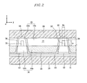
- FIG. 2 illustrates a vertical cross-sectional view taken along the line II-II of FIG. 1 ;
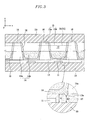
- FIG. 3 illustrates a vertical cross-sectional view taken along the line III-III of FIG. 1 ;
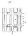
- FIG. 4 illustrates a horizontal cross-sectional view taken along the line IV-IV of FIG. 1 ;
- FIG. 5 illustrates a flow chart of a manufacturing process of a PDP according to an embodiment of the present invention.
- FIG. 6 to FIG. 11 illustrate cross-sectional views of stages in a method of manufacturing a rear substrate of the PDP according to an embodiment of the present invention.
- FIG. 1 illustrates a partial exploded perspective view of a PDP according to an embodiment of the present invention
- FIG. 2 illustrates a vertical cross-sectional view taken along the line II-II of FIG. 1
- FIG. 3 illustrates a vertical cross-sectional view taken along the line III-III of FIG. 1
- FIG. 4 illustrates a horizontal cross-sectional view taken along the line IV-IV of FIG. 1 .
- the PDP may include a first substrate 10 (hereinafter called a "rear substrate”) and a second substrate 20 (hereinafter called a “front substrate”) disposed facing each other with a predetermined space therebetween. Additionally, a plurality of discharge spaces 17 may be formed between the rear substrate 10 and the front substrate 20. A phosphor layer 19 may be formed in the discharge space 17.
- a discharge gas e.g., a gas mixture including neon (Ne) and xenon (Xe), may fill the discharge space 17.
- the phosphor layer 19 emits visible light after absorbing vacuum ultraviolet (VUV) rays generated by plasma discharge in the discharge gas.
- VUV vacuum ultraviolet
- An address electrode 11, a first electrode 31 (hereinafter, a “sustain electrode”) and a second electrode 32 (hereinafter, a “scan electrode”) may be disposed between the front substrate 20 and the rear substrate 10 to display an image.
- the address electrode 11 may be formed corresponding to each discharge space 17.
- the sustain electrode 31 and the scan electrode 32 may be disposed facing each other in a direction crossing the address electrode 11, corresponding to each discharge space 17.
- the sustain electrode 31 and the scan electrode 32 may be formed in the direction parallel to the address electrode 11.
- a structure of the sustain electrode 31 and the scan electrode 32 crossing the address electrode 11 will be described as an example.
- An address pulse may be applied to the address electrode 11 and a scan pulse may be applied to the scan electrode 32, generating address discharge.
- a discharge space 17 to be turned on may be selected by the address discharge.
- a sustain pulse may be reciprocally applied to the sustain electrode 31 and the scan electrode 32, generating a sustain discharge.
- the sustain discharge displays an image in the selected discharge space 17.
- a reset pulse having a voltage higher than a sustain pulse may be applied to the scan electrode 32 such that the sustain electrode 31 may be biased with a reference voltage.
- Each discharge space 17 may be reset by the reset pulse.
- the present invention is not limited to the above description, since each electrode may act differently according to a voltage applied thereto.
- the address electrode 11 may be formed on the inner surface of the rear substrate 10 and may extend in one direction, e.g., along a y-axis direction as shown in FIGS. 1-4 . Additionally, the address electrode 11 may be covered by a first dielectric layer 13. The first dielectric layer 13 may also cover the remaining part of the rear substrate 10. The address electrode 11 may be disposed parallel to other adjacent address electrodes 11, maintaining a space therebetween along an x-axis direction as shown in FIGS. 1-4 , i.e., corresponding to the discharge space 17.
- a first photosensitive material layer 12 may be formed on the first dielectric layer 13. As shown in FIG. 4 , the first photosensitive material layers 12 may be arranged with a predetermined spacing, corresponding to the address electrode 11. The first photosensitive material layer 12 may be covered by a second dielectric layer 14. The first photosensitive material layer 12 may protect the address electrode 11 from being etched. That is, when the discharge space 17 is being formed by etching the second dielectric layer 14 corresponding to the address electrode 11, the first photosensitive material layer 12 protects the address electrode 11 from being etched. Accordingly, the first photosensitive material layer 12 may be formed on the first dielectric layer 13 corresponding to the whole of the address electrodes 11. Additionally, a portion of the first photosensitive material layer 12 exposed to the etching may be removed after the etching.
- a width of the first photosensitive material layer 12 may be formed to be similar to a width of the second dielectric layer 14 partitioning the discharge space 17.
- the second dielectric layer 14 may be formed on the first photosensitive material layer 12 and the first dielectric layer 13 where the first photosensitive material layer 12 is not formed.
- the second dielectric layer 14 may partition the discharge space 17.
- the second dielectric layer 14 may partition the discharge space 17 in a lattice form as shown in the FIGS. 1-4 , or partition a discharge space in a stripe form (not shown).
- the second dielectric layer 14 may be formed only in a direction parallel to the first photosensitive material layer 12 (not shown).
- the second dielectric layer 14 may include a first member 14a and a second member 14b.
- the first member 14a may be disposed between the adjacent address electrodes 11 and may be elongated in parallel thereto.
- the second member 14b may be formed crossing the first member 14a, and corresponding to the sustain electrode 31 and the scan electrode 32.
- the second dielectric layer 14 may be formed in the y-axis direction parallel to the first photosensitive material layer 12, and formed in the x-axis direction crossing the first photosensitive material layer 12. Additionally, the second dielectric layer 14 may be formed by partially covering the first photosensitive material layer 12 at a part corresponding to the sustain electrode 31 and the scan electrode 32.
- a distance (h 1 ) from the rear substrate 10 to the first dielectric layer 13 corresponding to the address electrode 11 may be greater than a distance (h 2 ) from the rear substrate 10 to the first dielectric layer 13 formed at either edge of the discharge space 17.
- the distance from the rear substrate 10 to the bottom surface of the discharge space 17 may be greater than the distance from the rear substrate 10 to the bottom surface of the discharge space 17 adjacent to the first member 14a.
- the second dielectric layer 14 may be etched, e.g., by a sandblasting method, to form the discharge space 17. Due to the first photosensitive material layer 12, a part of the first dielectric layer 13 corresponding to the address electrode 11 is not affected by the etching. However, where the first photosensitive material layer 12 is not formed, i.e., at both edges of the discharge space 17, the first dielectric layer 13 may be affected by the sandblasting. Accordingly, after removing the first photosensitive material layer 12, a groove 13a may be formed on the bottom surface of both edges of the discharge space 17 in the first dielectric layer 13. The groove 13a may be parallel and adjacent to the first member 14a. When the phosphor layer 19 is provided in the discharge space, it may fill the groove 13a.
- the sustain electrode 31 and the scan electrode 32 may be disposed facing each other on the second dielectric layer 14.
- the sustain electrode 31 and the scan electrode 32 may be formed on the second member 14b and extend in the direction crossing the address electrode 11, i.e., the x-axis direction.
- the sustain electrode 31 and the scan electrode 32 may be disposed alternately on the first member 14a, along the direction parallel to the address electrode 11, i.e., the y-axis direction.
- a dimension (L h ) in the direction parallel to the substrate may be less than a dimension (L v ) perpendicular to the substrate.
- the facing area of the sustain electrode 31 and the scan electrode 32 is increased. Accordingly, an opposing discharge may be generated with a far lower voltage or a stronger discharge may be generated with the same voltage. That is, luminescence efficiency may be improved by the opposing discharge structure.
- the sustain electrode 31 and the scan electrode 32 are formed at both sides of the discharge space 17, light transmittance of the front substrate 20 may be improved.
- the electrodes may be formed of an opaque material having excellent electrical conductivity, .e.g., a metal.
- the sustain electrode 31 and the scan electrode 32 may be covered by the third dielectric layer 15. Additionally, a second photosensitive material layer 16 may be formed on the third dielectric layer 15. In FIG. 2 and FIG. 3 , the second photosensitive material layer 16 is drawn with a dotted line for convenience of explanation. However, the second photosensitive material layer 16 may be removed before completing the final product.
- the second photosensitive material layer 16 may protect the sustain electrode 31 and the scan electrode 32 from being etched. That is, like the first photosensitive material layer 12, when a discharge space 17 is formed between the sustain electrode 31 and the scan electrode 32 by etching the second dielectric layer 14 and the third dielectric layer 15, the second photosensitive material layer 16 protects the sustain electrode 31 and the scan electrode 32 from the etching. Accordingly, the second photosensitive material layer 16 may be used during a manufacturing process, and removed after etching the second dielectric layer 14 and the third dielectric layer 15.
- the second photosensitive material layer 16 may be formed as a stripe (not shown) corresponding to the sustain electrode 31 and scan electrode 32, and may be removed after use. Alternatively, as shown in FIGS. 2 and 3 , the second photosensitive material layer 16 may be formed as a lattice corresponding to the discharge space 17, and may be removed after use.
- the third dielectric layer 15 may include a third member 15a corresponding to the first member 14a of the second dielectric layer 14, and a fourth member 15b crossing the third member 15a and corresponding to the second member 14b.
- the second dielectric layer 14 and the third dielectric layer 15 may be formed of the same dielectric material. In this case, the manufacturing process may be simplified by use of the same material.
- the phosphor layer 19 may be formed on the inner surfaces of the first member 14a and the second member 14b of the second dielectric layer 14, and on the inner surface of the first dielectric layer 13 corresponding to the discharge space 17.
- the phosphor layer 19 may also be formed on the inner surfaces of the third member 15a and the fourth member 15b of the third dielectric layer 15 forming the discharge space 17 (not shown). As noted above, the phosphor layer 19 may fill the groove 13a.
- a protective layer 36 may be formed on the inner side surface of the third dielectric layer 15.
- the protective layer 36 may be formed at a part exposed to plasma discharge generated in the discharge space 17.
- the protective layer 36 may protect the third dielectric layer 15.
- the protective layer 36 requires a high secondary electron emission coefficient, but does not need to transmit visible light.
- the sustain electrode 31 and the scan electrode 32 may not be formed on the front substrate 20, but may be formed between the substrates 10 and 20, and the protective layer 36 is formed on the third dielectric layer 15 covering the sustain electrode 31 and the scan electrode 32.
- the protective layer 36 may be formed of a material that is opaque to visible light, e.g., an opaque MgO. Opaque MgO has a far higher secondary electron emission coefficient than MgO that is transparent to visible light, thereby allowing the discharge firing voltage to be further decreased.
- FIG. 5 illustrates a flow chart showing a manufacturing process of a PDP according to an exemplary embodiment of the present invention
- FIG. 6 to FIG. 11 illustrate cross-sectional views of stages in a method of manufacturing of a rear substrate of a PDP according to an exemplary embodiment of the present invention.
- step ST10 the rear substrate 10 is manufactured, and then, at step ST20, the second substrate 20 is separately manufactured. Electrodes, dielectric layers, and phosphor layers may be formed on the rear substrate 10. Details of forming elements on the rear substrate according to an embodiment of the present invention are shown in FIGS. 6-11 .
- the front substrate and the rear substrate may be combined and secured together.
- air may be evacuated from the discharge space 17 and a discharge gas, e.g. a mixed gas of Ne and Xe, fills the discharge space 17 to complete the PDP.
- a discharge gas e.g. a mixed gas of Ne and Xe
- the step ST10 of manufacturing the rear substrate may include forming the address electrode 11 as shown in FIG. 6 .
- Conventional methods e.g., a pattern printing method or an exposing and developing method utilizing photosensitive paste, may be used to manufacture the address electrode 11.
- the first dielectric layer 13 may be formed using a conventional printing method.
- the first photosensitive material layer 12 may be formed by providing a laminated film on the first dielectric layer 13. Subsequently, a patterning process may be performed by an exposure process so that the first photosensitive material layer 12 corresponding to the address electrode 11 remains.
- a second dielectric film 14' may be formed on the first photosensitive material layer 12 and the first dielectric layer 13.
- the second dielectric film 14' may be formed by a conventional printing method.
- the sustain electrode 31 and the scan electrode 32 may be formed on the second dielectric film 14'.
- the first photosensitive material layer 12 may be spaced apart from the sustain electrode 31 and the scan electrode 32.
- the sustain electrode 31 and the scan electrode 32 may be formed in a predetermined electrode pattern using pattern printing or a photosensitive material for a metal electrode.
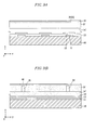
- the sustain electrode 31 and the scan electrode 32 may be covered with a third dielectric film 15' and the second photosensitive material layer 16 may be formed thereon, as shown in FIGS. 9A and 9B .
- the third dielectric film 15' may cover the sustain electrode 31 and the scan electrode 32, and may be formed on a part corresponding to a barrier rib partitioning the discharge space 17.
- the third dielectric film 15' and the second dielectric film 14' may be patterned to form the discharge space 17.
- the discharge space 17 may be defined by a dielectric material instead of a conventional material for the barrier rib.
- the third dielectric film 15' may be formed on the second dielectric film 14' by coating the dielectric material.
- a second photosensitive material film may be laminated on the third dielectric film 15'. Subsequently, a patterning process may be performed by utilizing an exposure process so that the second photosensitive material layer 16 remains at regions of the third dielectric film 15' corresponding to the sustain electrode 31 and the scan electrode 32 as shown in FIG. 9B .
- the discharge space 17 is partitioned by the remaining part of the second dielectric film 14' and the third dielectric film 15', i.e., the second dielectric layer 14 and the third dielectric layer 15.
- the second photosensitive material layer 16 as a mask and the first photosensitive material layer 12 as an etch stop, the second dielectric film 14' and the third dielectric film 15' may be removed to form the discharge space 17.
- the second photosensitive material layer 16 and the first photosensitive material layer 12 may be formed of a conventional laminated film for a barrier rib.
- the discharge space 17 may be formed by etching, e.g., using sandblasting the second dielectric film 14' and the third dielectric film 15'. After such etching, part of the second dielectric film 14' and the third dielectric film 15' not covered by the second photosensitive material layer 16, may be removed, i.e., the second photosensitive material layer 16 serves as a mask. By such removal, the first photosensitive material layer 12 may be exposed between the second dielectric layer 14 and the third dielectric layer 15, and the discharge space 17 may be formed.
- the first photosensitive material layer 12 may protect the first dielectric layer 13 and address electrode 11 from being removed during the etching, i.e., the first photosensitive material layer 12 serves as an etch stop.
- the sustain electrode 31 and scan electrode 32 may be formed on a partitioned location of the discharge space 17, and the discharge space 17 may be formed by etching the second dielectric layer 14 and the third dielectric layer 15 covering the sustain electrode 31 and the scan electrode 32. Accordingly, an opposing discharge structure of the sustain electrode 31 and the scan electrode 32 may be formed easily.
- any of the first photosensitive material layer 12 and the second photosensitive material layer 16 exposed by the etching may be removed, and the phosphor layer 19 may be formed inside the discharge space 17, as shown in FIG. 11 .
- the phosphor layer 19 may be formed by coating a phosphor, exposing and developing the phosphor. Phosphor may be applied to the inner surface of the second dielectric layer 14 partitioning the discharge space 17. Additionally, the phosphor may be applied to the inner surface of the second dielectric layer 14 and to the inner surface of the third dielectric layer 15.
- the manufacturing method of a PDP according to an exemplary embodiment of the present invention may further include forming the protective layer 36 on the inner surface of the third dielectric layer 15, as shown in FIG. 11 . That is, when the phosphor layer 19 is not formed on the inner surface of the third dielectric layer 15, a protective layer 36 may be formed thereon.
- an address electrode may be formed on a rear substrate, and a first photosensitive material layer may be formed on a first dielectric layer covering the address electrode. Additionally, a second dielectric layer may be formed on the first dielectric layer and the first photosensitive material layer, a first electrode and a second electrode may be formed on the second dielectric layer in an opposing discharge structure, and a second photosensitive material layer may be formed on a third dielectric layer covering the first electrode and the second electrode. Accordingly, regions of the second dielectric layer and the third dielectric layer on which a second photosensitive material layer is not formed are etched to the first photosensitive material layer, and thereby a discharge space is formed.
- the opposing discharge structure of the first electrode and the second electrode may be formed easily. Additionally, luminescence efficiency may be improved by the opposing discharge structure, and light transmittance may be improved by forming the first electrode and the second electrode at sides of the discharge space.
- first photosensitive layer is disclosed as a patterned layer
- first photosensitive layer may cover the first dielectric layer in its entirety. Accordingly, it will be understood by those of ordinary skill in the art that various changes in form and details may be made without departing from the scope of the present invention as set forth in the following claims.
Landscapes
- Engineering & Computer Science (AREA)
- Physics & Mathematics (AREA)
- Plasma & Fusion (AREA)
- Manufacturing & Machinery (AREA)
- Chemical & Material Sciences (AREA)
- Materials Engineering (AREA)
- Mechanical Engineering (AREA)
- Gas-Filled Discharge Tubes (AREA)
Claims (19)
- Écran d'affichage à plasma, comprenant :un premier substrat (10) ;une électrode d'adresse (11) formée sur le premier substrat (10) et s'étendant dans une première direction (y) ;une première couche diélectrique (13) couvrant l'électrode d'adresse (11) ;une deuxième couche diélectrique (14) sur la première couche diélectrique (13) ;une première électrode (31) et une deuxième électrode (32), disposées alternativement sur la deuxième couche diélectrique (14) et s'étendant dans une deuxième direction (x) ;une troisième couche diélectrique (15) couvrant la première électrode (31) et la deuxième électrode (32) ;un espace de décharge (17), l'espace de décharge (17) ayant un fond défini par la première couche diélectrique (13) située au fond de l'espace de décharge (17) et des parois latérales définies par les deuxième et troisième couches diélectriques (14, 15) ; etune couche de luminophore (19) dans l'espace de décharge (17) ;
caractérisé en ce quel'écran d'affichage à plasma comprend en outre une première couche de matériau photosensible (12) entre la première couche diélectrique (13) et la deuxième couche diélectrique (14). - Écran d'affichage à plasma selon la revendication 1, dans lequel la deuxième direction (x) est orthogonale à la première direction (y) et la première couche de matériau photosensible (12) est l'endroit de l'intersection entre la deuxième couche diélectrique (14) et l'électrode d'adresse (11).
- Écran d'affichage à plasma selon la revendication 1, dans lequel une largeur de la première couche de matériau photosensible (12) a substantiellement la même étendue que la largeur de la deuxième couche diélectrique (14), les largeurs étant mesurées dans la première direction (y).
- Écran d'affichage à plasma selon la revendication 1, dans lequel la deuxième couche diélectrique (14) comprend un premier élément (14a), disposé entre des électrodes d'adresse adjacentes (11) et s'étendant dans la première direction (y), et un deuxième élément (14b) orthogonal à et croisant l'électrode d'adresse (11).
- Écran d'affichage à plasma selon la revendication 4, dans lequel la troisième couche diélectrique (15) comprend un troisième élément (15a) correspondant au premier élément (14a) et un quatrième élément (15b) croisant le troisième élément (15a) et correspondant au deuxième élément (14b).
- Écran d'affichage à plasma selon la revendication 1, dans lequel la troisième couche diélectrique (15) possède une couche de protection (36) formée sur celle-ci, à l'intérieur de l'espace de décharge (17).
- Écran d'affichage à plasma selon la revendication 6, dans lequel la couche de protection (36) est opaque.
- Écran d'affichage à plasma selon la revendication 1, dans lequel la deuxième couche diélectrique (14) et la troisième couche diélectrique (15) sont formées du même matériau diélectrique.
- Écran d'affichage à plasma selon la revendication 1, dans lequel l'électrode d'adresse (11), la première électrode (31) et la deuxième électrode (32) sont formées d'un matériau conducteur opaque.
- Écran d'affichage à plasma selon la revendication 1, dans lequel, dans une coupe transversale de la première électrode (31) et de la deuxième électrode (32), une dimension (Lh) dans une direction horizontale de la première électrode (31) et de la deuxième électrode (32) est inférieure à une dimension (Lv) dans une direction verticale.
- Écran d'affichage à plasma selon la revendication 1, dans lequel la distance (h1) entre le premier substrat (10) et la première couche diélectrique (13) correspondant à l'électrode d'adresse (11) est supérieure à la distance (h2) entre le premier substrat (10) et la première couche diélectrique (13) placée de manière adjacente à la deuxième couche diélectrique (14), en parallèle avec l'électrode d'adresse (11).
- Écran d'affichage à plasma selon la revendication 1, comprenant en outre une rainure (13a) dans la première couche diélectrique (13), la rainure (13a) étant adjacente à une paroi latérale parmi les parois latérales de l'espace de décharge (17).
- Écran d'affichage à plasma selon la revendication 12, dans lequel la rainure (13a) est parallèle à l'électrode d'adresse (11).
- Écran d'affichage à plasma selon la revendication 1, dans lequel la première direction (y) est orthogonale à la deuxième direction (x) et la deuxième couche diélectrique (14) croise l'électrode d'adresse (11).
- Procédé de fabrication d'un écran d'affichage à plasma, comprenant les étapes consistant à :former une électrode d'adresse (11) sur un premier substrat (10) ;former une première couche diélectrique (13) sur l'électrode d'adresse (11) ;former une première couche de matériau photosensible (12) sur la première couche diélectrique (13) ;former un deuxième film diélectrique (14') sur la première couche de matériau photosensible (12) ;former des première et deuxième électrodes (31, 32) alternées sur le deuxième film diélectrique (14') ;former un troisième film diélectrique (15') sur les premières et deuxièmes électrodes (31, 32) ;former une deuxième couche de matériau photosensible (16) sur le troisième film diélectrique (15'), la deuxième couche de matériau photosensible (16) possédant un motif recouvrant la première électrode (31) et la deuxième électrode (32) ;former un espace de décharge (17) en gravant le deuxième film diélectrique (14') et le troisième film diélectrique (15') jusqu'à la première couche de matériau photosensible (12) en utilisant le motif de la deuxième couche de matériau photosensible (16) comme masque, l'espace de décharge (17) ayant des parois latérales définies par une deuxième couche diélectrique (14) et une troisième couche diélectrique (15) ; etformer une couche de luminophore (19) à l'intérieur de l'espace de décharge (17).
- Procédé selon la revendication 15, dans lequel la formation de l'espace de décharge (17) comprend en outre un sablage.
- Procédé selon la revendication 15, dans lequel la formation de la couche de luminophore (19) comprend en outre l'application de luminophore sur une surface intérieure de la deuxième couche diélectrique (14) formant l'espace de décharge (17) et sur une surface de la première couche diélec-trique (13) partagée par la deuxième couche diélectrique (14).
- Procédé selon la revendication 15, comprenant en outre la formation d'une couche de protection (36) sur des parois latérales de la troisième couche diélectrique (15).
- Procédé selon la revendication 15, comprenant en outre, avant la formation de la couche de luminophore (19), l'élimination de la première couche de matériau photosensible (12) et de la deuxième couche de matériau photosensible (16) qui sont exposées après la formation de l'espace de décharge (17).
Applications Claiming Priority (1)
| Application Number | Priority Date | Filing Date | Title |
|---|---|---|---|
| KR1020050024488A KR20060102653A (ko) | 2005-03-24 | 2005-03-24 | 플라즈마 디스플레이 패널 및 그 제조방법 |
Publications (2)
| Publication Number | Publication Date |
|---|---|
| EP1705681A1 EP1705681A1 (fr) | 2006-09-27 |
| EP1705681B1 true EP1705681B1 (fr) | 2009-07-01 |
Family
ID=35871090
Family Applications (1)
| Application Number | Title | Priority Date | Filing Date |
|---|---|---|---|
| EP05112475A Expired - Lifetime EP1705681B1 (fr) | 2005-03-24 | 2005-12-20 | Panneau d'affichage à plasma et son procédé de fabrication |
Country Status (6)
| Country | Link |
|---|---|
| US (1) | US7567032B2 (fr) |
| EP (1) | EP1705681B1 (fr) |
| JP (1) | JP2006269412A (fr) |
| KR (1) | KR20060102653A (fr) |
| CN (1) | CN100521048C (fr) |
| DE (1) | DE602005015185D1 (fr) |
Families Citing this family (2)
| Publication number | Priority date | Publication date | Assignee | Title |
|---|---|---|---|---|
| EP1912244A1 (fr) * | 2006-10-09 | 2008-04-16 | Carol Ann Wedding | Ecran plasma à colonnes tubulaires |
| WO2009050763A1 (fr) * | 2007-10-16 | 2009-04-23 | Hitachi, Ltd. | Panneau d'affichage à plasma |
Family Cites Families (12)
| Publication number | Priority date | Publication date | Assignee | Title |
|---|---|---|---|---|
| JPH07230756A (ja) | 1994-02-18 | 1995-08-29 | Oki Electric Ind Co Ltd | プラズマディスプレイパネルの陽極形成方法 |
| JP3224486B2 (ja) * | 1995-03-15 | 2001-10-29 | パイオニア株式会社 | 面放電型プラズマディスプレイパネル |
| TW320732B (fr) * | 1995-04-20 | 1997-11-21 | Matsushita Electron Co Ltd | |
| JPH08339766A (ja) | 1995-06-09 | 1996-12-24 | Fujitsu Ltd | プラズマパネル、その製造方法及び画像表示装置 |
| JPH10214569A (ja) * | 1997-01-31 | 1998-08-11 | Hitachi Ltd | プラズマディスプレイ装置 |
| TW392186B (en) * | 1997-12-01 | 2000-06-01 | Hitachi Ltd | Plasma display panel and image display using the same |
| JPH11233010A (ja) | 1998-02-13 | 1999-08-27 | Toppan Printing Co Ltd | 隔壁形成用基板及びその基板を用いた隔壁形成方法 |
| JP2000331615A (ja) | 1999-05-20 | 2000-11-30 | Fujitsu Ltd | プラズマディスプレイパネル及びその駆動方法 |
| TW493193B (en) * | 2001-05-30 | 2002-07-01 | Acer Display Tech Inc | AC plasma display panel |
| US7067979B2 (en) | 2001-10-02 | 2006-06-27 | Noritake Co., Limited | Gas-discharge display device and its manufacturing method |
| JP2003208853A (ja) | 2002-01-16 | 2003-07-25 | Noritake Co Ltd | ガス放電表示装置およびその製造方法 |
| JP3659913B2 (ja) * | 2001-10-30 | 2005-06-15 | 富士通株式会社 | プラズマディスプレイパネルおよびその製造方法 |
-
2005
- 2005-03-24 KR KR1020050024488A patent/KR20060102653A/ko not_active Ceased
- 2005-12-20 DE DE602005015185T patent/DE602005015185D1/de not_active Expired - Lifetime
- 2005-12-20 EP EP05112475A patent/EP1705681B1/fr not_active Expired - Lifetime
- 2005-12-28 CN CNB2005101284980A patent/CN100521048C/zh not_active Expired - Fee Related
- 2005-12-29 US US11/319,575 patent/US7567032B2/en not_active Expired - Fee Related
-
2006
- 2006-01-27 JP JP2006019675A patent/JP2006269412A/ja active Pending
Also Published As
| Publication number | Publication date |
|---|---|
| DE602005015185D1 (de) | 2009-08-13 |
| US20060214582A1 (en) | 2006-09-28 |
| US7567032B2 (en) | 2009-07-28 |
| CN100521048C (zh) | 2009-07-29 |
| JP2006269412A (ja) | 2006-10-05 |
| EP1705681A1 (fr) | 2006-09-27 |
| CN1838363A (zh) | 2006-09-27 |
| KR20060102653A (ko) | 2006-09-28 |
Similar Documents
| Publication | Publication Date | Title |
|---|---|---|
| EP1684322B1 (fr) | Panneau d'affichage à plasma | |
| US7567032B2 (en) | Plasma display panel and manufacturing method of the same | |
| US20060082307A1 (en) | Plasma display panel | |
| JP2006140144A (ja) | プラズマディスプレイパネル | |
| US20060290279A1 (en) | Plasma display panel | |
| KR100696635B1 (ko) | 플라즈마 디스플레이 패널 및 이의 제조방법 | |
| US7626334B2 (en) | Plasma display panel | |
| US7557506B2 (en) | Plasma display panel | |
| CN100521050C (zh) | 等离子体显示板 | |
| JP2006147556A (ja) | プラズマディスプレイパネル | |
| US7230380B2 (en) | Plasma display panel | |
| US20070007891A1 (en) | Plasma display panel | |
| KR100649233B1 (ko) | 플라즈마 디스플레이 패널 | |
| KR20060136150A (ko) | 플라즈마 디스플레이 패널 | |
| KR100589356B1 (ko) | 플라즈마 디스플레이 패널 | |
| US20090108730A1 (en) | Plasma Display Panel | |
| KR100709192B1 (ko) | 플라즈마 디스플레이 패널 및 그 제조 방법 | |
| KR100669378B1 (ko) | 플라즈마 디스플레이 패널 | |
| EP1717839A1 (fr) | Panneau d'affichage à plasma | |
| JP2006147533A (ja) | プラズマディスプレイパネル | |
| KR100766897B1 (ko) | 플라즈마 디스플레이 패널 및 이의 제조 방법 | |
| KR100739593B1 (ko) | 플라즈마 디스플레이 패널 및 그 제조방법 | |
| KR100697015B1 (ko) | 플라즈마 디스플레이 패널 및 그 제조 방법 | |
| KR100278785B1 (ko) | 플라즈마디스플레이패널의격벽제조방법 | |
| US20070046211A1 (en) | Plasma display panel |
Legal Events
| Date | Code | Title | Description |
|---|---|---|---|
| PUAI | Public reference made under article 153(3) epc to a published international application that has entered the european phase |
Free format text: ORIGINAL CODE: 0009012 |
|
| AK | Designated contracting states |
Kind code of ref document: A1 Designated state(s): AT BE BG CH CY CZ DE DK EE ES FI FR GB GR HU IE IS IT LI LT LU LV MC NL PL PT RO SE SI SK TR |
|
| AX | Request for extension of the european patent |
Extension state: AL BA HR MK YU |
|
| 17P | Request for examination filed |
Effective date: 20070326 |
|
| 17Q | First examination report despatched |
Effective date: 20070425 |
|
| AKX | Designation fees paid |
Designated state(s): DE FR GB NL |
|
| R17C | First examination report despatched (corrected) |
Effective date: 20071004 |
|
| GRAP | Despatch of communication of intention to grant a patent |
Free format text: ORIGINAL CODE: EPIDOSNIGR1 |
|
| GRAS | Grant fee paid |
Free format text: ORIGINAL CODE: EPIDOSNIGR3 |
|
| GRAA | (expected) grant |
Free format text: ORIGINAL CODE: 0009210 |
|
| AK | Designated contracting states |
Kind code of ref document: B1 Designated state(s): DE FR GB NL |
|
| REG | Reference to a national code |
Ref country code: GB Ref legal event code: FG4D |
|
| REF | Corresponds to: |
Ref document number: 602005015185 Country of ref document: DE Date of ref document: 20090813 Kind code of ref document: P |
|
| NLV1 | Nl: lapsed or annulled due to failure to fulfill the requirements of art. 29p and 29m of the patents act | ||
| PG25 | Lapsed in a contracting state [announced via postgrant information from national office to epo] |
Ref country code: NL Free format text: LAPSE BECAUSE OF FAILURE TO SUBMIT A TRANSLATION OF THE DESCRIPTION OR TO PAY THE FEE WITHIN THE PRESCRIBED TIME-LIMIT Effective date: 20090701 |
|
| PGFP | Annual fee paid to national office [announced via postgrant information from national office to epo] |
Ref country code: GB Payment date: 20091216 Year of fee payment: 5 Ref country code: FR Payment date: 20091221 Year of fee payment: 5 |
|
| PLBE | No opposition filed within time limit |
Free format text: ORIGINAL CODE: 0009261 |
|
| STAA | Information on the status of an ep patent application or granted ep patent |
Free format text: STATUS: NO OPPOSITION FILED WITHIN TIME LIMIT |
|
| 26N | No opposition filed |
Effective date: 20100406 |
|
| PGFP | Annual fee paid to national office [announced via postgrant information from national office to epo] |
Ref country code: DE Payment date: 20091217 Year of fee payment: 5 |
|
| GBPC | Gb: european patent ceased through non-payment of renewal fee |
Effective date: 20101220 |
|
| REG | Reference to a national code |
Ref country code: FR Ref legal event code: ST Effective date: 20110831 |
|
| PG25 | Lapsed in a contracting state [announced via postgrant information from national office to epo] |
Ref country code: FR Free format text: LAPSE BECAUSE OF NON-PAYMENT OF DUE FEES Effective date: 20110103 |
|
| PG25 | Lapsed in a contracting state [announced via postgrant information from national office to epo] |
Ref country code: GB Free format text: LAPSE BECAUSE OF NON-PAYMENT OF DUE FEES Effective date: 20101220 Ref country code: DE Free format text: LAPSE BECAUSE OF NON-PAYMENT OF DUE FEES Effective date: 20110701 |
|
| REG | Reference to a national code |
Ref country code: DE Ref legal event code: R119 Ref document number: 602005015185 Country of ref document: DE Effective date: 20110701 |