EP1705693A2 - Halbleitervorrichtung mit gestapelten Transistoren und Entkopplungskondensatoren - Google Patents
Halbleitervorrichtung mit gestapelten Transistoren und Entkopplungskondensatoren Download PDFInfo
- Publication number
- EP1705693A2 EP1705693A2 EP06005513A EP06005513A EP1705693A2 EP 1705693 A2 EP1705693 A2 EP 1705693A2 EP 06005513 A EP06005513 A EP 06005513A EP 06005513 A EP06005513 A EP 06005513A EP 1705693 A2 EP1705693 A2 EP 1705693A2
- Authority
- EP
- European Patent Office
- Prior art keywords
- layer
- transistor
- semiconductor device
- memory cell
- decoupling capacitor
- Prior art date
- Legal status (The legal status is an assumption and is not a legal conclusion. Google has not performed a legal analysis and makes no representation as to the accuracy of the status listed.)
- Granted
Links
Images



Classifications
-
- H—ELECTRICITY
- H10—SEMICONDUCTOR DEVICES; ELECTRIC SOLID-STATE DEVICES NOT OTHERWISE PROVIDED FOR
- H10B—ELECTRONIC MEMORY DEVICES
- H10B10/00—Static random access memory [SRAM] devices
- H10B10/12—Static random access memory [SRAM] devices comprising a MOSFET load element
- H10B10/125—Static random access memory [SRAM] devices comprising a MOSFET load element the MOSFET being a thin film transistor [TFT]
-
- A—HUMAN NECESSITIES
- A22—BUTCHERING; MEAT TREATMENT; PROCESSING POULTRY OR FISH
- A22C—PROCESSING MEAT, POULTRY, OR FISH
- A22C25/00—Processing fish ; Curing of fish; Stunning of fish by electric current; Investigating fish by optical means
- A22C25/17—Skinning fish
-
- A—HUMAN NECESSITIES
- A22—BUTCHERING; MEAT TREATMENT; PROCESSING POULTRY OR FISH
- A22C—PROCESSING MEAT, POULTRY, OR FISH
- A22C25/00—Processing fish ; Curing of fish; Stunning of fish by electric current; Investigating fish by optical means
- A22C25/08—Holding, guiding, or conveying fish before, during or after its preparation ; Devices for sizing fish; Automatically adapting conveyors or processing machines to the measured size
-
- A—HUMAN NECESSITIES
- A22—BUTCHERING; MEAT TREATMENT; PROCESSING POULTRY OR FISH
- A22C—PROCESSING MEAT, POULTRY, OR FISH
- A22C25/00—Processing fish ; Curing of fish; Stunning of fish by electric current; Investigating fish by optical means
- A22C25/20—Shredding; Cutting into cubes; Flaking
-
- H—ELECTRICITY
- H10—SEMICONDUCTOR DEVICES; ELECTRIC SOLID-STATE DEVICES NOT OTHERWISE PROVIDED FOR
- H10B—ELECTRONIC MEMORY DEVICES
- H10B10/00—Static random access memory [SRAM] devices
-
- H—ELECTRICITY
- H10—SEMICONDUCTOR DEVICES; ELECTRIC SOLID-STATE DEVICES NOT OTHERWISE PROVIDED FOR
- H10B—ELECTRONIC MEMORY DEVICES
- H10B10/00—Static random access memory [SRAM] devices
- H10B10/18—Peripheral circuit regions
-
- H—ELECTRICITY
- H10—SEMICONDUCTOR DEVICES; ELECTRIC SOLID-STATE DEVICES NOT OTHERWISE PROVIDED FOR
- H10D—INORGANIC ELECTRIC SEMICONDUCTOR DEVICES
- H10D88/00—Three-dimensional [3D] integrated devices
-
- H—ELECTRICITY
- H10—SEMICONDUCTOR DEVICES; ELECTRIC SOLID-STATE DEVICES NOT OTHERWISE PROVIDED FOR
- H10W—GENERIC PACKAGES, INTERCONNECTIONS, CONNECTORS OR OTHER CONSTRUCTIONAL DETAILS OF DEVICES COVERED BY CLASS H10
- H10W44/00—Electrical arrangements for controlling or matching impedance
- H10W44/601—Capacitive arrangements
-
- H—ELECTRICITY
- H10—SEMICONDUCTOR DEVICES; ELECTRIC SOLID-STATE DEVICES NOT OTHERWISE PROVIDED FOR
- H10B—ELECTRONIC MEMORY DEVICES
- H10B10/00—Static random access memory [SRAM] devices
- H10B10/12—Static random access memory [SRAM] devices comprising a MOSFET load element
-
- H—ELECTRICITY
- H10—SEMICONDUCTOR DEVICES; ELECTRIC SOLID-STATE DEVICES NOT OTHERWISE PROVIDED FOR
- H10B—ELECTRONIC MEMORY DEVICES
- H10B12/00—Dynamic random access memory [DRAM] devices
- H10B12/30—DRAM devices comprising one-transistor - one-capacitor [1T-1C] memory cells
- H10B12/31—DRAM devices comprising one-transistor - one-capacitor [1T-1C] memory cells having a storage electrode stacked over the transistor
-
- H—ELECTRICITY
- H10—SEMICONDUCTOR DEVICES; ELECTRIC SOLID-STATE DEVICES NOT OTHERWISE PROVIDED FOR
- H10B—ELECTRONIC MEMORY DEVICES
- H10B12/00—Dynamic random access memory [DRAM] devices
- H10B12/50—Peripheral circuit region structures
Definitions
- the invention relates to a semiconductor device having a stacked transistor structure, and to a related method of forming a decoupling capacitor.
- SRAM Static Random Access Memory
- decoupling capacitors disposed on a peripheral circuit region within a chip filter noises between operating supplies, e.g., power and ground.
- Decoupling capacitors disposed on the peripheral circuit region need to provide a large capacitance in a limited area.
- An example of a decoupling capacitor is a MOS (Metal Oxide Semiconductor) type capacitor.
- a gate oxide layer of the MOS transistor is used as a dielectric layer
- an impurity diffused region formed on a silicon substrate is used as a first electrode
- a gate layer formed of polysilicon can be used as a second electrode on the gate oxide layer.
- FIG. 1 A multilayer decoupling capacitor structure in a semiconductor memory device, such as a DRAM (Dynamic Random Access Memory), is shown in FIG. 1.
- a substrate layer and first, second and third polysilicon layers are used as an electrode of the capacitor, to form the multilayer decoupling capacitor.
- a first polysilicon electrode can be fabricated together with a gate electrode of a cell transistor formed within a memory cell region through a deposition process.
- Second polysilicon electrodes 62, 64, 72 and 74, and third polysilicon electrodes 60 and 70 are formed within the peripheral circuit region, through a separate process from the fabrication process performed in a memory cell region.
- the second polysilicon electrodes 62, 64, 72 and 74, and the third polysilicon electrodes 60 and 70, are formed through a separate deposition process in which the memory cell region is masked.
- a flow process to contact with n+ regions 76, 78 and 82 is needed.
- the separate deposition process causes a cost increase.
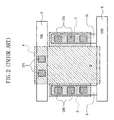
- FIG. 2 illustrates a layout of MOS capacitors that have been fabricated together with MOS transistors.
- a gate polysilicon region 4 is formed on an active region 2.
- the active region 2 is a region doped with n+ or p+ type impurity, and forms a first electrode.
- the gate polysilicon region 4 is a region doped with p+ or n+ type impurity, and forms a second electrode.
- a dielectric layer of the capacitor becomes a gate oxide layer interposed between a substrate on which the active region 2 and the gate polysilicon region 4 are formed.
- the gate polysilicon region 4 is electrically connected with a metal line 6 through a contact CN1, and the active region 2 is connected with metal lines 9, 10, and 8 through a contact CN2.
- the metal line 6 is a power line for transferring an operating power source voltage VDD
- the metal line 8 is a ground line for transferring a ground voltage GND to remove power noise and obtain reliable power.
- a decoupling capacitor of FIG. 2 is fabricated within the peripheral circuit region through the same process as a transistor of a cell region.
- the decoupling capacitor is a single capacitor disposed planarly.
- a decoupling capacitance of the decoupling capacitor of FIG. 2 is less than the decoupling capacitor of FIG. 1, and a decoupling loss can result from a short between the first and second electrodes.
- the MOS-type decoupling capacitor of FIG. 2 has a low capacitance in a highly-integrated semiconductor device.
- a manufacturing process technology for stack type semiconductor memory devices has been developed in conformity with the need for high integration, being changed from a planar layout structure of memory cell transistors of the memory cell region, e.g., in an SRAM.
- a stack type semiconductor device is fabricated comprising a single stacked memory cell, four N-type MOS transistors as pull-down and pass transistors formed on a semiconductor substrate layer among six MOS transistors constituting a memory cell, and two P-type MOS transistors as load transistors formed on another substrate layer, e.g., channel silicon layer which is insulatively formed on gate electrodes of the N-type MOS transistors.
- a semiconductor memory having stacked memory cells achieves high speed and low power, thus the need for removal of various kinds of signal noises and power noises is increased. Therefore, a need exists for a decoupling capacitor having improved capacitance in a limited area.
- the invention achieves this problem by providing a semiconductor device having the features of claim 1 and a method of forming a decoupling capacitor having the features of claim 21.
- Advantageous embodiments of the invention are mentioned in the dependent claims the wording of which is herewith incorporated into the description by reference to avoid unnecessary text repetition.
- a semiconductor device having a plurality of transistors formed on different layers comprises a stacked capacitor cluster, wherein a stacked capacitor of the stacked capacitor cluster comprises an insulation layer of a respective one of the plurality of transistors and a first conduction layer and a second conduction layer disposed above and below the insulation layer, respectively, wherein the stacked capacitor is a decoupling capacitor of the stacked capacitor cluster connected in parallel between a first line and a second line.
- capacitor cluster refers to a group of two or more capacitors connected with each other, e.g., in parallel or in series.
- One capacitor cluster of the stack type can include at least three decoupling capacitors.
- the first line may be a power source voltage line, and the second line may be a ground voltage line.
- the first line may be a signal line, and the second line may be a ground voltage line.
- a first decoupling capacitor comprises a gate oxide layer of MOS transistor as a first dielectric layer
- a second decoupling capacitor comprises a first top gate insulation layer formed on a first channel silicon layer, as a second dielectric layer, the first channel silicon layer being positioned on the MOS transistor
- a third decoupling capacitor comprises a second top gate insulation layer formed on a second channel silicon layer, as a third dielectric layer, the second channel silicon layer being positioned on the first top gate insulation layer.
- a first decoupling capacitor comprises a gate oxide layer of MOS transistor as a first dielectric layer
- a second decoupling capacitor comprises an interlayer insulation layer formed on a gate electrode of the MOS transistor, as a second dielectric layer
- a third decoupling capacitor comprises a first top gate insulation layer formed on a first channel silicon layer, as a third dielectric layer, the first channel silicon layer being positioned on the interlayer insulation layer
- a fourth decoupling capacitor comprises an interlayer insulation layer formed on a first top gate, as a fourth dielectric layer, the first top gate being formed on the first top gate insulation layer
- a fifth decoupling capacitor comprises a second top gate insulation layer formed on a second channel silicon layer, as a fifth dielectric layer, the second channel silicon layer being positioned on the fourth dielectric layer.
- CMOS SRAM cell In applying a design rule under about 80 nm, six transistors constituting a full CMOS SRAM cell can be disposed on different layers.
- a size of decoupling capacitors disposed on a peripheral circuit region should be reduced according to the reduction in cell pitch.
- a capacitance value is also reduced, thus a technique for reducing only the size of the decoupling capacitor without substantially reducing a capacitance value is needed.
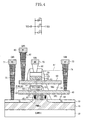
- FIGS. 3 and 4 an exemplary structure of decoupling capacitor having a double stack type is shown in FIGS. 3 and 4.
- a gate polysilicon layer 42 is formed on an active region 30 of a substrate in which a DN well 10, a P well 20, and n+ doped regions are formed.
- a first channel silicon layer 45, a second channel silicon layer 60 and a first metal layer 80 are formed sequentially thereof.
- the first channel silicon layer 45 and the second channel silicon layer 60 are used as a transistor substrate.
- the gate polysilicon layer 42 can be used for the formation of a gate electrode of a pull-down transistor
- a first top gate layer 52 formed on the first channel silicon layer 45 can be used for the formation of a gate electrode of load transistor.
- a second top gate layer 63 formed on the second channel silicon layer 60 can be formed for the formation of a gate electrode of pass transistor.
- transistors constituting a memory cell are disposed on three layers, thus a planar size is reduced about two to three times or more.
- a conductive layer formed on a memory cell region and peripheral circuit region is patterned functions as a substrate or gate electrode on the memory cell region, and functions as an electrode of decoupling capacitor on the peripheral circuit region.
- first and second channel silicon layers 45 and 60 and first and second top gate layers 52 and 63 of the double stack type memory cell are utilized as electrodes of decoupling capacitors.
- a capacitor cluster of the double stack type memory cell shown in FIGS. 3 and 4 comprises insulation layers 40, 50 and 61 and conduction layers 30, 42, 45, 52, 60 and 63.
- the double stack type memory cell comprises decoupling capacitors C1, C2 and C3.
- the insulation layers 40, 50 and 61, the conduction layers 30, 42, 45, 51, 60 and 63 positioned on upper and lower layers from the boundary of the insulation layers, and the decoupling capacitors C1, C2 and C3 are respectively connected in parallel between first and second lines VDD and GND.
- the double stack type memory cell further includes a metal silicide layer 64, formed by a reaction to refractory metal material such as tungsten to reduce a resistance, a hard mask layer 65 and a tungsten contact 66.
- capacitor clusters are provided in a peripheral circuit region of chip, being connected with power lines and various reference signals.
- the power source voltage (VDD) line and the ground voltage (GND) line can be used for other signals, wherein for example, the first line can be a signal line to transfer various signals of a semiconductor device, and the second line can be a ground voltage line.
- a first decoupling capacitor C1 shown in FIG. 4 is formed by using a gate oxide layer 40 of MOS transistor as a first dielectric layer.
- a second decoupling capacitor C2 is formed by using a first top gate insulation layer 50 formed on a first channel silicon layer 45 as a second dielectric layer, the first channel silicon layer 45 being positioned on the MOS transistor.
- a third decoupling capacitor C3 is formed by using a second top gate insulation layer 61 formed on a second channel silicon layer 60 as a third dielectric layer, the second channel silicon layer 60 being positioned on the first top gate insulation layer 50.
- a first electrode (bottom electrode in the drawing) of first decoupling capacitor C1 is an active region 30 doped with n+ type impurity
- a second electrode (top electrode in the drawing) is a gate polysilicon layer 42 doped with p+ type impurity
- a first electrode (a bottom electrode in the drawing) of second decoupling capacitor C2 is a first channel silicon layer 45
- a second electrode (top electrode in the drawing) is a first top gate 51.
- a first electrode (bottom electrode in the drawing) of third decoupling capacitor C3 is a second channel silicon layer 60
- a second electrode (top electrode in the drawing) is a second top gate 63.
- the ground voltage GND is coupled with the active region 30, the first top gate 51 and the second channel silicon layer 60, and the power source voltage VDD is coupled with the gate polysilicon layer 42, the first channel silicon layer 45 and the second top gate 63.
- the first and second top gate insulation layers 50 and 61 can be formed of TEOS, silicon dioxide, silicon nitride layer, or a composite layer of materials selected from these materials. Other materials may be used having a high dielectric constant, as the dielectric material of the capacitor, and are well known to those skilled in the art.
- the polysilicon layer is doped, and a surface layer of the polysilicon layer can become silicided, e.g., titanium silicide, tungsten silicide. Meanwhile, a sidewall connector (CNT) layer 53 electrically connects the first top gate 51 and a tungsten contact 75.
- CNT sidewall connector
- the active region 30 is connected to a metal zero layer 71 through a tungsten contact WC 75, and the metal zero layer 71 is coupled with the ground voltage GND.
- the metal zero layer 71 may be a metal damascene layer formed of material such as tungsten.
- First contacts CO1 shown in FIG. 3 are metal contacts connected with the tungsten contact 75 and the metal zero layer 71. Details for a metal damascene process are widely known in the art, thus a detailed description for the damascene process is omitted.
- the first channel silicon layer 45 formed on a selective epitaxial growth (SEG) layer 43 is connected to metal zero layer 72 through tungsten contact WC 74, to function as a bottom electrode of the second decoupling capacitor C2.
- the metal zero layer 72 is coupled with the power source voltage VDD.
- the second channel silicon layer 60 formed on a selective epitaxial growth (SEG) layer 54 is connected to a first metal layer M1, 80 through a metal contact MC 82, to function as a bottom electrode of the third decoupling capacitor C3.
- the first metal layer 80 can be formed of metal material such as Aluminum, and is connected to the power source voltage.
- Second contacts CO2 shown in FIG. 3 nest contacts and metal contacts MC.
- the metal contact MC is connected to the first metal layer M1, 80, and to the nest contacts.
- the nest contacts are formed in a lower part of the metal contacts, and have a contact plug that electrically connects with an upper part or side part of the second channel silicon layer 60.
- FIG. 4 shows a second decoupling capacitor C2 comprising the CS1 layer 45 and TG1 52 as electrode layers, and a third decoupling capacitor C3 comprising the CS2 layer 60 and TG2 63 as electrode layers.
- the second decoupling capacitor C2 and the third decoupling capacitor C3 are stacked on a first decoupling capacitor C1 comprising an n-type MOS capacitor in a peripheral circuit region or field region.
- the CS1 layer 45 is biased with VDD
- the TG1 layer 52 is biased with GND
- the TG2 layer 63 with VDD The CS1 layer, the TG1 layer, the CS2 layer and the TG2 layer are representative of an equivalent circuit having three capacitors connected with one another in parallel shown in the upper part of FIG. 4.
- three decoupling capacitors connected in parallel can be fabricated together with the fabrication of memory cells without a specific additional process, and a layout area of peripheral circuit region on which the decoupling capacitors are formed is substantially reduced planarly.
- FIG. 5 depicts a sectional structure of stack-type decoupling capacitor according to an exemplary embodiment of the invention, wherein two decoupling capacitors are added so as to obtain a capacitor cluster having a large capacitance.
- a semiconductor memory also employs a double stacked memory cell, wherein a P-type MOS transistor is formed on a first layer as a MOS layer.
- five decoupling capacitors C1-C5 form a stack structure connected between the power source voltage VDD and the ground voltage VSS.
- the decoupling capacitor C1 of a lowermost layer is constructed of a PMOS capacitor, and the CS1 layer 45 is biased with GND, the TG1 layer 52 is biased with VDD, the CS2 layer 60 is biased with VDD and the TG2 layer 63 is biased with GND.
- a first decoupling capacitor C1 is formed by using the gate oxide layer 40 of MOS transistor as a first dielectric layer; the second decoupling capacitor C2 is formed by using an interlayer insulation layer 44 formed on the gate electrode 42 of the MOS transistor, as a second dielectric layer; the third decoupling capacitor C3 is formed by using the first top gate insulation layer 50 formed on the first channel silicon layer 45, as a third dielectric layer, the first channel silicon layer 45 being positioned on the interlayer insulation layer 44; a fourth decoupling capacitor C4 is formed by using an interlayer insulation layer 56 formed on the first top gate 52, as a fourth dielectric layer, the first top gate 52 being formed on the first top gate insulation layer; and a fifth decoupling capacitor C5 is formed by using the second top gate insulation layer 61 formed on the second channel silicon layer 60, as a fifth dielectric layer, the second channel silicon layer 60 being positioned on the fourth dielectric layer.
- An active region 31 comprises p+ doped portions in a N well 21 of a substrate, and is biased with VDD, the gate polysilicon layer 42 with GND, the CS1 layer 45 with VDD, the TG1 layer 52 with GND, the CS2 layer 60 with VDD, the TG2 63 with a GND.
- load transistors are formed as a first layer, and thereon, a pull-down transistor and a pass transistor are disposed.
- a method of forming the structure of FIG. 5 is substantially similar to the case of FIG. 4, except for the type of transistor and the supply of bias.
Landscapes
- Life Sciences & Earth Sciences (AREA)
- Engineering & Computer Science (AREA)
- Wood Science & Technology (AREA)
- Zoology (AREA)
- Food Science & Technology (AREA)
- Semiconductor Integrated Circuits (AREA)
- Semiconductor Memories (AREA)
Applications Claiming Priority (1)
| Application Number | Priority Date | Filing Date | Title |
|---|---|---|---|
| KR1020050023228A KR100665848B1 (ko) | 2005-03-21 | 2005-03-21 | 적층 타입 디커플링 커패시터를 갖는 반도체 장치 |
Publications (3)
| Publication Number | Publication Date |
|---|---|
| EP1705693A2 true EP1705693A2 (de) | 2006-09-27 |
| EP1705693A3 EP1705693A3 (de) | 2008-01-23 |
| EP1705693B1 EP1705693B1 (de) | 2019-09-25 |
Family
ID=36295511
Family Applications (1)
| Application Number | Title | Priority Date | Filing Date |
|---|---|---|---|
| EP06005513.4A Expired - Lifetime EP1705693B1 (de) | 2005-03-21 | 2006-03-17 | Halbleitervorrichtung mit gestapelten Transistoren und Entkopplungskondensatoren |
Country Status (5)
| Country | Link |
|---|---|
| US (1) | US7999297B2 (de) |
| EP (1) | EP1705693B1 (de) |
| JP (1) | JP2006270101A (de) |
| KR (1) | KR100665848B1 (de) |
| CN (1) | CN100546033C (de) |
Cited By (2)
| Publication number | Priority date | Publication date | Assignee | Title |
|---|---|---|---|---|
| EP2131397A1 (de) | 2008-06-02 | 2009-12-09 | Commissariat a L'Energie Atomique | In drei Richtungen integrierter Transistorschaltkreis mit einer dynamisch anpassbaren Schwellenspannung (VT) |
| US8013399B2 (en) | 2008-06-02 | 2011-09-06 | Commissariat A L'energie Atomique | SRAM memory cell having transistors integrated at several levels and the threshold voltage VT of which is dynamically adjustable |
Families Citing this family (21)
| Publication number | Priority date | Publication date | Assignee | Title |
|---|---|---|---|---|
| US7999299B2 (en) | 2005-06-23 | 2011-08-16 | Samsung Electronics Co., Ltd. | Semiconductor memory device having capacitor for peripheral circuit |
| KR101275758B1 (ko) | 2007-07-20 | 2013-06-14 | 삼성전자주식회사 | 복수개의 적층된 트랜지스터들을 구비하는 반도체 소자 및그 제조방법 |
| KR100951742B1 (ko) | 2007-12-26 | 2010-04-08 | 주식회사 동부하이텍 | 반도체 소자 레이아웃 방법 |
| KR101444381B1 (ko) | 2008-09-30 | 2014-11-03 | 삼성전자주식회사 | 파워 디커플링 커패시터를 포함하는 반도체 메모리 장치 및그것의 제조 방법 |
| KR101046993B1 (ko) | 2008-12-05 | 2011-07-06 | 주식회사 하이닉스반도체 | 저장 커패시터 어레이 회로 |
| US9425192B2 (en) * | 2008-12-11 | 2016-08-23 | Altera Corporation | Integrated circuit decoupling capacitors |
| KR101143634B1 (ko) * | 2010-09-10 | 2012-05-11 | 에스케이하이닉스 주식회사 | 캐패시터 형성 방법과 이를 이용한 반도체 소자 |
| US8697567B2 (en) | 2012-05-22 | 2014-04-15 | International Business Machines Corporation | Implementing decoupling devices inside a TSV DRAM stack |
| TWI566328B (zh) | 2013-07-29 | 2017-01-11 | 高效電源轉換公司 | 具有用於產生附加構件之多晶矽層的氮化鎵電晶體 |
| EP3054618B1 (de) * | 2013-09-30 | 2019-11-06 | Panasonic Intellectual Property Management Co., Ltd. | Kommunikationsvorrichtung und motorsteuerungsvorrichtung |
| TWI538226B (zh) * | 2013-12-13 | 2016-06-11 | 華亞科技股份有限公司 | 具有高結構強度之堆疊型電容器之製造方法 |
| JP6545976B2 (ja) * | 2014-03-07 | 2019-07-17 | 株式会社半導体エネルギー研究所 | 半導体装置 |
| KR102446164B1 (ko) * | 2017-12-26 | 2022-09-22 | 삼성전자주식회사 | 부하 스탠다드 셀을 포함하는 집적 회로 및 그 설계 방법 |
| JP6988688B2 (ja) * | 2018-05-21 | 2022-01-05 | 株式会社デンソー | 半導体装置 |
| US11462568B2 (en) * | 2018-06-22 | 2022-10-04 | Intel Corporation | Stacked thin film transistors |
| WO2020051144A1 (en) * | 2018-09-05 | 2020-03-12 | Tokyo Electron Limited | Architecture design and processes for manufacturing monolithically integrated 3d cmos logic and memory |
| US11616053B2 (en) * | 2018-09-05 | 2023-03-28 | Tokyo Electron Limited | Method to vertically route a logic cell incorporating stacked transistors in a three dimensional logic device |
| WO2020055642A2 (en) * | 2018-09-05 | 2020-03-19 | Tokyo Electron Limited | Power distribution network for 3d logic and memory |
| CN110060998B (zh) * | 2019-04-29 | 2022-05-17 | 厦门天马微电子有限公司 | 一种反相电路结构、栅极驱动电路及显示面板 |
| CN111048662A (zh) * | 2019-12-26 | 2020-04-21 | 上海华虹宏力半导体制造有限公司 | 并联pps电容器的制作方法及并联pps电容器 |
| WO2025065635A1 (en) * | 2023-09-28 | 2025-04-03 | Huawei Technologies Co., Ltd. | Stacked structure, pixel driving circuit, control circuit, display module and electronic device |
Citations (1)
| Publication number | Priority date | Publication date | Assignee | Title |
|---|---|---|---|---|
| US5851868A (en) | 1995-09-19 | 1998-12-22 | Samsung Electronics Co., Ltd. | Methods of forming integrated decoupling capacitors |
Family Cites Families (11)
| Publication number | Priority date | Publication date | Assignee | Title |
|---|---|---|---|---|
| JPH04170069A (ja) * | 1990-11-02 | 1992-06-17 | Hitachi Ltd | 半導体記憶装置 |
| US5675185A (en) | 1995-09-29 | 1997-10-07 | International Business Machines Corporation | Semiconductor structure incorporating thin film transistors with undoped cap oxide layers |
| US5739576A (en) | 1995-10-06 | 1998-04-14 | Micron Technology, Inc. | Integrated chip multilayer decoupling capacitors |
| JPH09307067A (ja) * | 1996-05-16 | 1997-11-28 | Oki Electric Ind Co Ltd | セミカスタム半導体集積回路装置 |
| US6054359A (en) | 1999-06-14 | 2000-04-25 | Taiwan Semiconductor Manufacturing Company | Method for making high-sheet-resistance polysilicon resistors for integrated circuits |
| US6475838B1 (en) | 2000-03-14 | 2002-11-05 | International Business Machines Corporation | Methods for forming decoupling capacitors |
| US6492244B1 (en) | 2001-11-21 | 2002-12-10 | International Business Machines Corporation | Method and semiconductor structure for implementing buried dual rail power distribution and integrated decoupling capacitance for silicon on insulator (SOI) devices |
| US6608365B1 (en) | 2002-06-04 | 2003-08-19 | Lsi Logic Corporation | Low leakage PMOS on-chip decoupling capacitor cells compatible with standard CMOS cells |
| JP2004031785A (ja) * | 2002-06-27 | 2004-01-29 | Fujitsu Ltd | 半導体装置及び半導体装置の設計方法 |
| US6737699B2 (en) | 2002-06-27 | 2004-05-18 | Intel Corporation | Enhanced on-chip decoupling capacitors and method of making same |
| JP2004288786A (ja) | 2003-03-20 | 2004-10-14 | Renesas Technology Corp | 半導体装置 |
-
2005
- 2005-03-21 KR KR1020050023228A patent/KR100665848B1/ko not_active Expired - Fee Related
-
2006
- 2006-03-08 US US11/370,365 patent/US7999297B2/en active Active
- 2006-03-17 EP EP06005513.4A patent/EP1705693B1/de not_active Expired - Lifetime
- 2006-03-21 CN CNB2006100681291A patent/CN100546033C/zh not_active Expired - Lifetime
- 2006-03-22 JP JP2006079541A patent/JP2006270101A/ja active Pending
Patent Citations (1)
| Publication number | Priority date | Publication date | Assignee | Title |
|---|---|---|---|---|
| US5851868A (en) | 1995-09-19 | 1998-12-22 | Samsung Electronics Co., Ltd. | Methods of forming integrated decoupling capacitors |
Cited By (3)
| Publication number | Priority date | Publication date | Assignee | Title |
|---|---|---|---|---|
| EP2131397A1 (de) | 2008-06-02 | 2009-12-09 | Commissariat a L'Energie Atomique | In drei Richtungen integrierter Transistorschaltkreis mit einer dynamisch anpassbaren Schwellenspannung (VT) |
| US8013399B2 (en) | 2008-06-02 | 2011-09-06 | Commissariat A L'energie Atomique | SRAM memory cell having transistors integrated at several levels and the threshold voltage VT of which is dynamically adjustable |
| US8183630B2 (en) | 2008-06-02 | 2012-05-22 | Commissariat A L'energie Atomique | Circuit with transistors integrated in three dimensions and having a dynamically adjustable threshold voltage VT |
Also Published As
| Publication number | Publication date |
|---|---|
| JP2006270101A (ja) | 2006-10-05 |
| KR20060101685A (ko) | 2006-09-26 |
| EP1705693B1 (de) | 2019-09-25 |
| KR100665848B1 (ko) | 2007-01-09 |
| EP1705693A3 (de) | 2008-01-23 |
| US7999297B2 (en) | 2011-08-16 |
| US20060208299A1 (en) | 2006-09-21 |
| CN1848436A (zh) | 2006-10-18 |
| CN100546033C (zh) | 2009-09-30 |
Similar Documents
| Publication | Publication Date | Title |
|---|---|---|
| EP1705693B1 (de) | Halbleitervorrichtung mit gestapelten Transistoren und Entkopplungskondensatoren | |
| US12444705B2 (en) | Memory devices and related electronic systems | |
| CN100468621C (zh) | 包含电容器的集成电路装置及制造方法 | |
| US7833847B2 (en) | Method of forming semiconductor device having stacked transistors | |
| WO2022261596A1 (en) | Microelectronic devices, related electronic systems, and methods of forming microelectronic devices | |
| US12159866B2 (en) | Semiconductor integrated circuit device | |
| CN114245938B (zh) | 具有穿过半导体材料立柱的栅极材料的集成晶体管,及形成集成晶体管的方法 | |
| KR100843272B1 (ko) | 반도체 집적회로장치 | |
| KR20100095242A (ko) | 반도체 소자 및 그 제조 방법 | |
| KR101356329B1 (ko) | 가변 미앤더 라인 저항 | |
| US11894039B2 (en) | Fft-dram | |
| US20090065837A1 (en) | Semiconductor memory device having capacitor for peripheral circuit | |
| JPH09116027A (ja) | 半導体装置及びその製造方法 | |
| US6661048B2 (en) | Semiconductor memory device having self-aligned wiring conductor | |
| US8263456B2 (en) | Methods of manufacturing capacitor and semiconductor device including the same | |
| US11569218B2 (en) | Semiconductor integrated circuit device | |
| US20070023838A1 (en) | Fabricating logic and memory elements using multiple gate layers | |
| CN120282442A (zh) | 半导体器件和半导体结构 | |
| JP2025014023A (ja) | スタンダードセル構造 | |
| JP2004031886A (ja) | コンタクトの製造方法 | |
| KR20100042462A (ko) | 주변회로용 커패시터를 구비하는 반도체 메모리 소자 | |
| US20260107574A1 (en) | Multi-stack semiconductor device including channel structures having different channel widths | |
| JP5687317B2 (ja) | 半導体装置の製造方法 |
Legal Events
| Date | Code | Title | Description |
|---|---|---|---|
| PUAI | Public reference made under article 153(3) epc to a published international application that has entered the european phase |
Free format text: ORIGINAL CODE: 0009012 |
|
| AK | Designated contracting states |
Kind code of ref document: A2 Designated state(s): AT BE BG CH CY CZ DE DK EE ES FI FR GB GR HU IE IS IT LI LT LU LV MC NL PL PT RO SE SI SK TR |
|
| AX | Request for extension of the european patent |
Extension state: AL BA HR MK YU |
|
| PUAL | Search report despatched |
Free format text: ORIGINAL CODE: 0009013 |
|
| AK | Designated contracting states |
Kind code of ref document: A3 Designated state(s): AT BE BG CH CY CZ DE DK EE ES FI FR GB GR HU IE IS IT LI LT LU LV MC NL PL PT RO SE SI SK TR |
|
| AX | Request for extension of the european patent |
Extension state: AL BA HR MK YU |
|
| RIC1 | Information provided on ipc code assigned before grant |
Ipc: H01L 21/02 20060101AFI20060524BHEP Ipc: H01L 23/64 20060101ALI20071219BHEP Ipc: H01L 27/06 20060101ALI20071219BHEP Ipc: H01L 27/11 20060101ALI20071219BHEP Ipc: H01L 23/522 20060101ALI20071219BHEP Ipc: H01L 21/8244 20060101ALI20071219BHEP Ipc: H01L 27/108 20060101ALN20060524BHEP Ipc: H01L 27/105 20060101ALI20071219BHEP |
|
| 17P | Request for examination filed |
Effective date: 20080519 |
|
| 17Q | First examination report despatched |
Effective date: 20080623 |
|
| AKX | Designation fees paid |
Designated state(s): DE FR GB |
|
| RAP1 | Party data changed (applicant data changed or rights of an application transferred) |
Owner name: SAMSUNG ELECTRONICS CO., LTD. |
|
| GRAP | Despatch of communication of intention to grant a patent |
Free format text: ORIGINAL CODE: EPIDOSNIGR1 |
|
| INTG | Intention to grant announced |
Effective date: 20190405 |
|
| GRAS | Grant fee paid |
Free format text: ORIGINAL CODE: EPIDOSNIGR3 |
|
| GRAA | (expected) grant |
Free format text: ORIGINAL CODE: 0009210 |
|
| AK | Designated contracting states |
Kind code of ref document: B1 Designated state(s): DE FR GB |
|
| REG | Reference to a national code |
Ref country code: GB Ref legal event code: FG4D |
|
| REG | Reference to a national code |
Ref country code: DE Ref legal event code: R096 Ref document number: 602006058618 Country of ref document: DE |
|
| REG | Reference to a national code |
Ref country code: DE Ref legal event code: R097 Ref document number: 602006058618 Country of ref document: DE |
|
| PLBE | No opposition filed within time limit |
Free format text: ORIGINAL CODE: 0009261 |
|
| STAA | Information on the status of an ep patent application or granted ep patent |
Free format text: STATUS: NO OPPOSITION FILED WITHIN TIME LIMIT |
|
| 26N | No opposition filed |
Effective date: 20200626 |
|
| PG25 | Lapsed in a contracting state [announced via postgrant information from national office to epo] |
Ref country code: FR Free format text: LAPSE BECAUSE OF NON-PAYMENT OF DUE FEES Effective date: 20200331 |
|
| P01 | Opt-out of the competence of the unified patent court (upc) registered |
Effective date: 20230520 |
|
| PGFP | Annual fee paid to national office [announced via postgrant information from national office to epo] |
Ref country code: DE Payment date: 20250121 Year of fee payment: 20 |
|
| PGFP | Annual fee paid to national office [announced via postgrant information from national office to epo] |
Ref country code: GB Payment date: 20250123 Year of fee payment: 20 |
|
| REG | Reference to a national code |
Ref country code: DE Ref legal event code: R079 Ref document number: 602006058618 Country of ref document: DE Free format text: PREVIOUS MAIN CLASS: H01L0021020000 Ipc: H10P0095000000 |
|
| REG | Reference to a national code |
Ref country code: DE Ref legal event code: R071 Ref document number: 602006058618 Country of ref document: DE |
|
| REG | Reference to a national code |
Ref country code: GB Ref legal event code: PE20 Expiry date: 20260316 |