EP1705708A2 - Detektorvorrichtung und ihr Herstellungsverfahren - Google Patents
Detektorvorrichtung und ihr Herstellungsverfahren Download PDFInfo
- Publication number
- EP1705708A2 EP1705708A2 EP06251563A EP06251563A EP1705708A2 EP 1705708 A2 EP1705708 A2 EP 1705708A2 EP 06251563 A EP06251563 A EP 06251563A EP 06251563 A EP06251563 A EP 06251563A EP 1705708 A2 EP1705708 A2 EP 1705708A2
- Authority
- EP
- European Patent Office
- Prior art keywords
- pixel array
- layer
- radiation
- conversion layer
- radiation conversion
- Prior art date
- Legal status (The legal status is an assumption and is not a legal conclusion. Google has not performed a legal analysis and makes no representation as to the accuracy of the status listed.)
- Ceased
Links
- 238000004519 manufacturing process Methods 0.000 title claims abstract description 40
- 238000000034 method Methods 0.000 title claims description 17
- 230000005855 radiation Effects 0.000 claims abstract description 78
- 238000006243 chemical reaction Methods 0.000 claims abstract description 64
- 230000003287 optical effect Effects 0.000 claims abstract description 16
- 238000002601 radiography Methods 0.000 description 9
- 238000003384 imaging method Methods 0.000 description 7
- 238000007689 inspection Methods 0.000 description 6
- OAICVXFJPJFONN-UHFFFAOYSA-N Phosphorus Chemical compound [P] OAICVXFJPJFONN-UHFFFAOYSA-N 0.000 description 5
- 239000000835 fiber Substances 0.000 description 5
- 239000000463 material Substances 0.000 description 5
- 230000008901 benefit Effects 0.000 description 4
- 238000000151 deposition Methods 0.000 description 4
- 230000008021 deposition Effects 0.000 description 4
- 238000009659 non-destructive testing Methods 0.000 description 4
- 239000013307 optical fiber Substances 0.000 description 4
- 238000000429 assembly Methods 0.000 description 3
- 230000000712 assembly Effects 0.000 description 3
- 238000002591 computed tomography Methods 0.000 description 3
- 229910021417 amorphous silicon Inorganic materials 0.000 description 2
- 238000005253 cladding Methods 0.000 description 2
- 238000000576 coating method Methods 0.000 description 2
- 230000001066 destructive effect Effects 0.000 description 2
- 238000010586 diagram Methods 0.000 description 2
- 239000002184 metal Substances 0.000 description 2
- 229910052751 metal Inorganic materials 0.000 description 2
- 229910003016 Lu2SiO5 Inorganic materials 0.000 description 1
- 238000002441 X-ray diffraction Methods 0.000 description 1
- 238000004458 analytical method Methods 0.000 description 1
- 238000003491 array Methods 0.000 description 1
- 230000002238 attenuated effect Effects 0.000 description 1
- 239000011248 coating agent Substances 0.000 description 1
- 238000010276 construction Methods 0.000 description 1
- 230000008878 coupling Effects 0.000 description 1
- 238000010168 coupling process Methods 0.000 description 1
- 238000005859 coupling reaction Methods 0.000 description 1
- 229910021419 crystalline silicon Inorganic materials 0.000 description 1
- 230000007547 defect Effects 0.000 description 1
- 230000000694 effects Effects 0.000 description 1
- 230000002708 enhancing effect Effects 0.000 description 1
- 230000008020 evaporation Effects 0.000 description 1
- 238000001704 evaporation Methods 0.000 description 1
- 230000005284 excitation Effects 0.000 description 1
- 230000004907 flux Effects 0.000 description 1
- 229910003443 lutetium oxide Inorganic materials 0.000 description 1
- KJLLKLRVCJAFRY-UHFFFAOYSA-N mebutizide Chemical compound ClC1=C(S(N)(=O)=O)C=C2S(=O)(=O)NC(C(C)C(C)CC)NC2=C1 KJLLKLRVCJAFRY-UHFFFAOYSA-N 0.000 description 1
- 230000007246 mechanism Effects 0.000 description 1
- 230000008569 process Effects 0.000 description 1
- 230000004044 response Effects 0.000 description 1
- 238000004544 sputter deposition Methods 0.000 description 1
- 238000003860 storage Methods 0.000 description 1
Images


Classifications
-
- G—PHYSICS
- G01—MEASURING; TESTING
- G01T—MEASUREMENT OF NUCLEAR OR X-RADIATION
- G01T1/00—Measuring X-radiation, gamma radiation, corpuscular radiation, or cosmic radiation
- G01T1/16—Measuring radiation intensity
- G01T1/20—Measuring radiation intensity with scintillation detectors
- G01T1/2018—Scintillation-photodiode combinations
- G01T1/20185—Coupling means between the photodiode and the scintillator, e.g. optical couplings using adhesives with wavelength-shifting fibres
-
- H—ELECTRICITY
- H10—SEMICONDUCTOR DEVICES; ELECTRIC SOLID-STATE DEVICES NOT OTHERWISE PROVIDED FOR
- H10F—INORGANIC SEMICONDUCTOR DEVICES SENSITIVE TO INFRARED RADIATION, LIGHT, ELECTROMAGNETIC RADIATION OF SHORTER WAVELENGTH OR CORPUSCULAR RADIATION
- H10F39/00—Integrated devices, or assemblies of multiple devices, comprising at least one element covered by group H10F30/00, e.g. radiation detectors comprising photodiode arrays
- H10F39/10—Integrated devices
- H10F39/12—Image sensors
- H10F39/18—Complementary metal-oxide-semiconductor [CMOS] image sensors; Photodiode array image sensors
- H10F39/189—X-ray, gamma-ray or corpuscular radiation imagers
Definitions
- the invention relates generally to inspection systems and more specifically to radiographic inspection techniques and assemblies.
- X-rays are transmitted through an object and converted into light of corresponding intensity using a light production layer.
- the light generated by the light production layer is provided to an electronic device.
- the electronic device is adapted to convert the light signals generated by the light production layer to corresponding electrical signals.
- the electrical signals are then used to construct an image of the object.
- X-ray scatter In radiography, X-ray scatter undesirably reduces (or fogs) the resulting image.
- lead grids are used on the detector to provide geometric rejection of the scattered, secondary X-rays.
- higher energy X-rays are used, so grids are not always adequate.
- Compton scatter from an object can be a large part of the X-ray flux impinging on the X-ray film cassette.
- a metallic plate or screen may be employed, to filter the lower energy Compton scattered radiation.
- the film can be further intensified by the photoelectrons emitted from the metallic plate when the plate is in intimate contact with said film.
- This enables a high spatial transfer of the X-ray pattern to the film. In nondestructive testing at X-ray energies above 150 kV, this is the primary mechanism for darkening the film, as the film is essentially transparent to X-rays in this regime.
- a similar benefit is experienced with computed radiography, where metal screens are placed in intimate contact with the computed radiography image plates. In digital radiography, metal screens have been placed on the back surface (the side toward the X-rays) of X-ray phosphor screens, especially under X-ray energies of 1 MeV and above. In such an embodiment, the phosphor is typically viewed by a digital or analog camera.
- the metallic plate or screen it would be desirable for the metallic plate or screen to shield the electronic device from impinging X-rays.
- the metallic plate or screen may not provide the desired electron intensification and scatter rejection in the MeV energy range.
- the metallic plate or screen is of higher thickness to provide the required shielding while maintaining the intensification benefits.
- a detector assembly includes a radiation conversion layer configured to receive radiation passing through an object and to convert the radiation to a plurality of signals, and a pixel array configured for receiving the signals representative of the radiation passing through the object.
- the pixel array is further configured for generating a corresponding image of the object.
- the radiation conversion layer is directly coupled to the pixel array.
- a detector assembly in another embodiment, includes a radiation conversion layer configured to receive radiation passing through an object, a light production layer configured to convert the radiation to corresponding optical signals representative of the radiation passing through the object and a pixel array directly coupled to the light production layer and configured for receiving the corresponding optical signals.
- the pixel array is further configured for generating a corresponding image of the object.
- the detector assembly also includes a contact layer disposed between the light production layer and the pixel array, the contact layer being configured to direct the optical signals to the pixel array.
- a method for forming a detector assembly includes disposing a radiation conversion layer over a pixel array to form the detector assembly, wherein the radiation conversion layer is in direct contact with the pixel array.
- Fig. 1 is a diagrammatic view of a direct conversion embodiment of a detector assembly implemented according to one aspect of the invention.
- detector assembly 10 includes a radiation conversion layer 12 and a pixel array 14. Each layer is described in further detail below.
- Radiation conversion layer 12 is configured to receive radiation 5 such as X-rays passing through an object (not shown) and convert the radiation to a plurality of signals.
- the radiation conversion layer 12 comprises at least one metallic layer (also indicated by reference numeral 12).
- the thickness of the metallic layer 12 ranges from about 50 microns to about 2 millimeters.
- "about” should be understood to represent an accuracy of plus or minus ten percent (10%) of the recited lengths.
- pixel array, 14 is a direct conversion pixel array, which is configured to receive the signals that represent radiation passing through the radiation conversion layer and to generate the corresponding image of the object.
- signals include primary X-rays, unattenuated X-rays, fluorescence X-rays and secondary electrons. Secondary electrons may be photoelectrons, Compton electrons, and Auger electrons.
- the radiation conversion layer 12 is directly coupled to the pixel array 14.
- the radiation conversion layer 12 includes at least one metallic layer, and the metallic layer is directly coupled to the pixel array 14.
- Fig. 2 illustrates an indirect conversion embodiment of the invention.
- the detector assembly 10 further includes a light production layer 16 disposed between the radiation conversion layer 12 and the pixel array 14.
- the light production layer 16 is configured to receive the radiation passing through the radiation conversion layer and to generate corresponding optical signals.
- Exemplary light production layers 16 are formed from X-ray phosphor materials, non-limiting examples of which include Gd202S:(Tb, Pr), Y1.34Gd0.60O3:(Eu,Pr)0.06 (HILIGHT), Lu2O3:(Eu3+, Tb), CsI:TI, NaI:TI, CsI:Na, Y203:Eu3+, Gd203:Eu, CdW04, BGO (Bi4Ge3O12), LSO (Lu2SiO5:Ce), GSO (Gd2SiO5:Ce), YAP(YAlO3:Ce), LuAP (LuAlO3:Ce), LPS (Lu2Si2O7:Ce) and combinations thereof. This list is meant to be illustrative and not exhaustive. Other phosphors are also applicable.
- the pixel array 14 is a light sensitive pixel array configured for receiving the optical signals.
- a patterned radiation conversion layer thick layers of scintillators (light production material) for example, in a range of about 50 microns to about 2 millimeters can be used, as light spread can be controlled in a patterned manner.
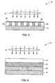
- the radiation conversion layer comprises a patterned radiation conversion layer 13 as illustrated in Fig. 3.
- the radiation conversion layer 12 is disposed in a pattern and the spaces between the radiation conversion layers are filled with light production material.
- the patterned radiation conversion layer is encapsulated within a metallic layer 15.
- the patterned metallic layer 12 improves spatial resolution, while offering control of both X-ray scatter and electron scatter within the metallic plate.
- electrons and fluorescence X rays from the radiation conversion layer result in the creation of optical photons in the light production material, which are captured by the pixel array 14.
- direct X rays may create optical photons in the light production layer and contribute to the total light captured by pixel array 14.
- the light production layer is coated onto the radiation conversion layer, which may be a metallic layer.
- the light production layer is directly coupled to the radiation conversion layer.
- the light production layer 16 includes scintillator needles (not shown) grown onto the radiation conversion layer, which can be achieved through a technique known in the art as a CsI:TI deposition, for the particular CsI:TI phosphor.
- the radiation conversion layer 12 can also be deposited onto the light production layer 16 by techniques such as evaporation and sputtering.
- the light production layer 16 may be coated onto the pixel array 14 by any assortment of settling, or coating techniques, as mentioned above. Following the deposition, the radiation conversion layer 12 may be placed directly onto the coated phosphor.
- Fig. 5 illustrates an indirect conversion embodiment of the detector assembly that includes a radiation conversion layer 12, a light production layer 16, a contact layer 18, and a pixel array 14.
- the light production layer 16 is disposed between the radiation conversion layer 12 and the contact layer 18.
- a thickness of the contact layer 18 is greater than that of the radiation conversion layer 12.
- the radiation conversion layer and the pixel array may be implemented as described with reference to Fig. 1.
- the contact layer 18 is described in further detail below.
- Contact layer 18 is disposed between the light production layer and the pixel array.
- the contact layer is configured to direct the optical signals to the pixel array.
- the contact layer may include several optical fibers or a fiber optical plate. The contact layer shields the pixel array from damage and direct excitation that may propagate through the light production layer and the radiation conversion layer.
- the contact layer comprises optical fibers
- a cladding surrounds each optical fiber.
- the optical fiber filters off-angle, highly scattered light thus enhancing the contrast from an otherwise degraded image exiting the light production layer.
- the off angle light is absorbed in black material inserted into the detector 10 as either black fibers of black coatings around each fiber or cladding.
- the numerical aperture may be selected to reduce off-angle light accordingly.
- the contact layer is about 6 millimeters thick.
- the radiation conversion layer comprises at least one metallic layer.
- the radiation conversion layer 12 is coupled to the pixel array 14 via the light production layer 16 and the contact layer 18.
- the combination of the metallic radiation conversion layer 12 or patterned intensification layer 13 and the fiber optic component 18 offers a compact design that enables the construction of thin assemblies that can be placed into restricted spaces in objects of interest to perform nondestructive testing.
- the pixel array may include any one of charge coupled device arrays, CMOS imagers, amorphous silicon photodiodes and crystalline silicon photodiodes, micro-channel plate based imaging devices and position sensitive gas detectors.
- Fig. 5 is a block diagram of an embodiment of system 30, which is an X-ray system designed both to acquire original image data and to process the image data for display and analysis in accordance with the present technique.
- Other imaging systems such as computed tomography systems, laminography systems, and digital radiography systems, which acquire three dimensional data for a volume, also benefit from the present techniques.
- X-ray system 10 is merely an example of one such implementation and is not intended to be limiting in terms of modality.
- adapted to refers to devices in a system to allow the elements of the system to cooperate to provide a described effect; these terms also refer to operation capabilities of electrical or optical elements such as analog or digital computers or application specific devices (such as an application specific integrated circuit (ASIC)), amplifiers or the like that are programmed to provide an output in response to given input signals, and to mechanical devices for optically or electrically coupling components together.
- ASIC application specific integrated circuit
- X-ray system 30 includes an X-ray source 32 configured to emit X-ray radiation through object 34.
- X-ray source 32 may be a conventional X-ray tube producing X-rays having both high energy and low energy X-rays.
- the end-point energy of the X-rays varies from about 30 keV to about 16 MeV.
- the X-rays continue through object 34 and, after being attenuated by the object, impinge upon detector assembly 10.
- Detector assembly may be implemented using any of the techniques described with reference to Fig. 1 to Fig. 4.
- Processor 38 receives signals from the detector assembly 10 and is configured to generate an image corresponding to the object being scanned.
- the processor is configured to determine an X-ray path geometry and determine an energy deposition profile for at least one segment of each of the X-ray paths.
- the processor is further configured to generate an image of the object based on the energy deposition profile and the X-ray paths.
- computer 40 communicates with processor 38 to enable an operator, using operator console 42, to view the generated image.
- the operator may view the image on display unit 44.
- the generated image may also be stored in storage device 46 which may include hard drives, floppy discs, compact discs, etc.
- the operator may also use computer 40 to provide commands and instructions to source controller 48.
- Source controller 48 provides power and timing signals to X-ray source 32.
- the X-ray system can be used for various non-destructive applications in digital radiography systems or computed tomography systems.
- Such applications might include inspection of turbine blades and fan blades inside a jet engine, where high image contrast is needed to detect the smallest defect in these components, while a small detector is desired which is small enough to enter between the blades to reach an inspection location.
- Other applications include nondestructive testing methods using digital radiography systems, laminography systems, and computed tomography systems.
- the above described techniques have many advantages including small size, high efficiency and better shielding for the pixel array.
- the radiation conversion layer is placed in contact with the light production layer, and is directly coupled to the imaging device such as amorphous silicon, a CCD, CMOS imaging device, micro-channel plate based imaging devices, and position sensitive gas detectors, the size of the detector is substantially reduced.
- the detector assembly also has increased efficiency for capturing light, and thus has a rapid decrease in exposure time.
- the radiation conversion layer also offers shielding to the imaging devices mentioned above.
- the radiation conversion layer, the light production layer and/or the intermediary fiber optic plate (thickness, numerical aperture, other scatter enhancement elements in the faceplate) may be interchanged on the imaging device to optimize performance for specific applications of interest.
Landscapes
- Physics & Mathematics (AREA)
- Health & Medical Sciences (AREA)
- Life Sciences & Earth Sciences (AREA)
- General Physics & Mathematics (AREA)
- High Energy & Nuclear Physics (AREA)
- Molecular Biology (AREA)
- Spectroscopy & Molecular Physics (AREA)
- Measurement Of Radiation (AREA)
- Light Receiving Elements (AREA)
- Solid State Image Pick-Up Elements (AREA)
Applications Claiming Priority (1)
| Application Number | Priority Date | Filing Date | Title |
|---|---|---|---|
| US11/090,675 US7214947B2 (en) | 2005-03-25 | 2005-03-25 | Detector assembly and method of manufacture |
Publications (2)
| Publication Number | Publication Date |
|---|---|
| EP1705708A2 true EP1705708A2 (de) | 2006-09-27 |
| EP1705708A3 EP1705708A3 (de) | 2010-08-04 |
Family
ID=36607588
Family Applications (1)
| Application Number | Title | Priority Date | Filing Date |
|---|---|---|---|
| EP06251563A Ceased EP1705708A3 (de) | 2005-03-25 | 2006-03-23 | Detektorvorrichtung und ihr Herstellungsverfahren |
Country Status (4)
| Country | Link |
|---|---|
| US (1) | US7214947B2 (de) |
| EP (1) | EP1705708A3 (de) |
| JP (1) | JP5247988B2 (de) |
| CN (1) | CN1837795B (de) |
Cited By (3)
| Publication number | Priority date | Publication date | Assignee | Title |
|---|---|---|---|---|
| CN102667579A (zh) * | 2009-09-15 | 2012-09-12 | 恩迪斯外科影像有限公司 | 用于图像的修正、测量和显示的方法和系统 |
| US8952980B2 (en) | 2010-08-09 | 2015-02-10 | Gsi Group, Inc. | Electronic color and luminance modification |
| EP3356859A4 (de) * | 2015-10-02 | 2019-08-14 | Varian Medical Systems, Inc. | Bildgebungsvorrichtung mit hoher dqe |
Families Citing this family (21)
| Publication number | Priority date | Publication date | Assignee | Title |
|---|---|---|---|---|
| US7358502B1 (en) * | 2005-05-06 | 2008-04-15 | David Appleby | Devices, systems, and methods for imaging |
| US7263165B2 (en) * | 2005-07-14 | 2007-08-28 | Siemens Medical Solutions Usa, Inc. | Flat panel detector with KV/MV integration |
| US7920758B2 (en) * | 2006-11-22 | 2011-04-05 | Tektronix, Inc. | Measurement apparatus and method of measurement of video spatial scale, offset and cropping |
| US7625502B2 (en) * | 2007-03-26 | 2009-12-01 | General Electric Company | Nano-scale metal halide scintillation materials and methods for making same |
| US7708968B2 (en) | 2007-03-26 | 2010-05-04 | General Electric Company | Nano-scale metal oxide, oxyhalide and oxysulfide scintillation materials and methods for making same |
| US7608829B2 (en) * | 2007-03-26 | 2009-10-27 | General Electric Company | Polymeric composite scintillators and method for making same |
| US8129686B2 (en) | 2007-09-12 | 2012-03-06 | Morpho Detection, Inc. | Mask for coded aperture systems |
| US7915591B2 (en) * | 2007-09-12 | 2011-03-29 | Morpho Detection, Inc. | Mask for coded aperture systems |
| US8693613B2 (en) * | 2010-01-14 | 2014-04-08 | General Electric Company | Nuclear fuel pellet inspection |
| US8493569B2 (en) | 2010-12-27 | 2013-07-23 | Mitutoyo Corporation | Optical encoder readhead configuration with phosphor layer |
| US10914847B2 (en) * | 2011-01-18 | 2021-02-09 | Minnesota Imaging And Engineering Llc | High resolution imaging system for digital dentistry |
| US9429521B2 (en) * | 2012-05-30 | 2016-08-30 | Board Of Trustees Of Michigan State University | Plant phenometrics systems and methods and devices related thereto |
| US9016560B2 (en) | 2013-04-15 | 2015-04-28 | General Electric Company | Component identification system |
| US20160141318A1 (en) * | 2013-06-28 | 2016-05-19 | Teledyne Dalsa, Inc. | Method and system for assembly of radiological imaging sensor |
| US9442261B2 (en) * | 2014-07-09 | 2016-09-13 | Toshiba Medical Systems Corporation | Devices for coupling a light-emitting component and a photosensing component |
| WO2016176612A1 (en) | 2015-04-29 | 2016-11-03 | Board Of Trustees Of Michigan State University | Methods for estimating photosynthetic characteristics in plant canopies and systems and apparatus related thereto |
| JP6321703B2 (ja) * | 2016-03-04 | 2018-05-09 | ファナック株式会社 | ワイヤ放電加工機の検査システム |
| US10365383B2 (en) | 2016-09-09 | 2019-07-30 | Minnesota Imaging And Engineering Llc | Structured detectors and detector systems for radiation imaging |
| WO2019103997A1 (en) * | 2017-11-24 | 2019-05-31 | Saint-Gobain Ceramics & Plastics, Inc. | Substrate including scintillator materials, system including substrate, and method of use |
| JP7225383B2 (ja) * | 2019-04-24 | 2023-02-20 | 富士フイルム株式会社 | 放射線画像撮影装置 |
| TWI714391B (zh) * | 2019-12-13 | 2020-12-21 | 晉原光電有限公司 | 用於感測消除靜電的x光機的感測器 |
Citations (1)
| Publication number | Priority date | Publication date | Assignee | Title |
|---|---|---|---|---|
| US20020159563A1 (en) | 2001-04-27 | 2002-10-31 | Canon Kabushiki Kaisha | Radiation imaging apparatus and radiation imaging system using the same |
Family Cites Families (18)
| Publication number | Priority date | Publication date | Assignee | Title |
|---|---|---|---|---|
| US3389255A (en) * | 1964-03-04 | 1968-06-18 | Dainippon Toryo Kk | Intensifying screens |
| BE792387A (nl) * | 1971-12-31 | 1973-06-07 | Agfa Gevaert Nv | Versterkingsschermen voor rontgenfotografie |
| US5198673A (en) * | 1992-01-23 | 1993-03-30 | General Electric Company | Radiation image detector with optical gain selenium photosensors |
| US5430298A (en) * | 1994-06-21 | 1995-07-04 | General Electric Company | CT array with improved photosensor linearity and reduced crosstalk |
| FR2737017B1 (fr) * | 1995-07-17 | 1997-08-29 | Centre Nat Rech Scient | Detecteur de particules sensible a la position |
| US5663005A (en) * | 1995-08-08 | 1997-09-02 | Agfa-Gevaert, N.V. | Self-supporting or supported phosphor screen or panel |
| JPH0998970A (ja) * | 1995-10-06 | 1997-04-15 | Canon Inc | X線撮像装置 |
| JP3332200B2 (ja) * | 1995-11-29 | 2002-10-07 | 日立金属株式会社 | X線ct用放射線検出器 |
| US5650626A (en) * | 1996-07-16 | 1997-07-22 | Eastman Kodak Company | X-ray imaging detector with thickness and composition limited substrate |
| KR100638915B1 (ko) * | 1998-12-14 | 2006-10-25 | 하마마츠 포토닉스 가부시키가이샤 | 광학소자 및 이것을 사용한 방사선 검출기 |
| EP1300694B1 (de) * | 2000-05-19 | 2011-03-23 | Hamamatsu Photonics K.K. | Strahlungsdetektor und verfahren zu seiner herstellung |
| JP2002122672A (ja) * | 2000-10-12 | 2002-04-26 | Canon Inc | 撮像装置及びこれを備える放射線撮像システム |
| US6835936B2 (en) * | 2001-02-07 | 2004-12-28 | Canon Kabushiki Kaisha | Scintillator panel, method of manufacturing scintillator panel, radiation detection device, and radiation detection system |
| FR2848677B1 (fr) * | 2002-12-17 | 2005-04-15 | Trixell Sas | Detecteur de rayonnement x a l'etat solide |
| US7112802B2 (en) * | 2003-04-11 | 2006-09-26 | Canon Kabushiki Kaisha | Scintillator panel, radiation detecting apparatus, and radiation detection system |
| US7098460B2 (en) | 2003-08-04 | 2006-08-29 | General Electric Company | Monolithic structure for x-ray CT collimator |
| US6996209B2 (en) * | 2003-10-27 | 2006-02-07 | Ge Medical Systems Global Technology Company, Llc | Scintillator coatings having barrier protection, light transmission, and light reflection properties |
| US7177389B2 (en) * | 2004-01-09 | 2007-02-13 | Adelphi Technology | X-ray tomography and laminography |
-
2005
- 2005-03-25 US US11/090,675 patent/US7214947B2/en not_active Expired - Fee Related
-
2006
- 2006-03-23 EP EP06251563A patent/EP1705708A3/de not_active Ceased
- 2006-03-24 CN CN2006100673789A patent/CN1837795B/zh not_active Expired - Fee Related
- 2006-03-24 JP JP2006082220A patent/JP5247988B2/ja not_active Expired - Fee Related
Patent Citations (1)
| Publication number | Priority date | Publication date | Assignee | Title |
|---|---|---|---|---|
| US20020159563A1 (en) | 2001-04-27 | 2002-10-31 | Canon Kabushiki Kaisha | Radiation imaging apparatus and radiation imaging system using the same |
Cited By (4)
| Publication number | Priority date | Publication date | Assignee | Title |
|---|---|---|---|---|
| CN102667579A (zh) * | 2009-09-15 | 2012-09-12 | 恩迪斯外科影像有限公司 | 用于图像的修正、测量和显示的方法和系统 |
| US8952980B2 (en) | 2010-08-09 | 2015-02-10 | Gsi Group, Inc. | Electronic color and luminance modification |
| EP3356859A4 (de) * | 2015-10-02 | 2019-08-14 | Varian Medical Systems, Inc. | Bildgebungsvorrichtung mit hoher dqe |
| US11156727B2 (en) | 2015-10-02 | 2021-10-26 | Varian Medical Systems, Inc. | High DQE imaging device |
Also Published As
| Publication number | Publication date |
|---|---|
| CN1837795B (zh) | 2012-05-16 |
| JP2006276014A (ja) | 2006-10-12 |
| EP1705708A3 (de) | 2010-08-04 |
| US20060214109A1 (en) | 2006-09-28 |
| CN1837795A (zh) | 2006-09-27 |
| US7214947B2 (en) | 2007-05-08 |
| JP5247988B2 (ja) | 2013-07-24 |
Similar Documents
| Publication | Publication Date | Title |
|---|---|---|
| US7214947B2 (en) | Detector assembly and method of manufacture | |
| JP4208687B2 (ja) | イメージセンサ | |
| US5150394A (en) | Dual-energy system for quantitative radiographic imaging | |
| US9791385B2 (en) | Modular high resolution X-ray computed tomography system | |
| US20070290135A1 (en) | Imaging assembly and inspection method | |
| JP2003265457A (ja) | X線画像化方法とx線画像化システム | |
| US20110110490A1 (en) | Method and apparatus for x-ray radiographic imaging | |
| EP0061496A1 (de) | Detektor-system mit bildverstärker für elektronische röntgenaufnahmen. | |
| WO1991011813A1 (en) | Detector arrangement for a ct device | |
| CN112713163A (zh) | 双能辐射平板探测器、制备方法及探测系统 | |
| JPH034156B2 (de) | ||
| Nagarkar et al. | High resolution X-ray sensor for non-destructive evaluation | |
| CN1991575B (zh) | 计算机放射摄影系统及使用方法 | |
| JP2002257939A (ja) | 2次元放射線検出器とその製造方法、及びその補正方法 | |
| JP5060548B2 (ja) | ラジオグラフィ測定装置及びラジオグラフィ測定方法 | |
| EP0092157A1 (de) | Zweidimensionaler Strahlungsdetektor | |
| JP2008051626A (ja) | ラインセンサ、ラインセンサユニット及び放射線非破壊検査システム | |
| JP2008251211A (ja) | イメージインテンシファイア | |
| EP1422538A2 (de) | Röntgengerat | |
| JP2001188096A (ja) | 2次元アレイ型放射線検出器及びx線遮蔽壁の製造方法 | |
| McClain et al. | Digital Imaging–Real-Time, Computed, and Digital Radiography | |
| Bueno et al. | Hybrid scintillators for x-ray imaging | |
| JP2019163970A (ja) | シンチレータアレイ、放射線検出器および放射線コンピュータ断層撮影装置 | |
| Tate et al. | CCD detectors | |
| JP2017044588A (ja) | X線検出器およびx線撮像システム |
Legal Events
| Date | Code | Title | Description |
|---|---|---|---|
| PUAI | Public reference made under article 153(3) epc to a published international application that has entered the european phase |
Free format text: ORIGINAL CODE: 0009012 |
|
| AK | Designated contracting states |
Kind code of ref document: A2 Designated state(s): AT BE BG CH CY CZ DE DK EE ES FI FR GB GR HU IE IS IT LI LT LU LV MC NL PL PT RO SE SI SK TR |
|
| AX | Request for extension of the european patent |
Extension state: AL BA HR MK YU |
|
| PUAL | Search report despatched |
Free format text: ORIGINAL CODE: 0009013 |
|
| AK | Designated contracting states |
Kind code of ref document: A3 Designated state(s): AT BE BG CH CY CZ DE DK EE ES FI FR GB GR HU IE IS IT LI LT LU LV MC NL PL PT RO SE SI SK TR |
|
| AX | Request for extension of the european patent |
Extension state: AL BA HR MK YU |
|
| 17P | Request for examination filed |
Effective date: 20110204 |
|
| AKX | Designation fees paid |
Designated state(s): DE FR GB |
|
| 17Q | First examination report despatched |
Effective date: 20110323 |
|
| STAA | Information on the status of an ep patent application or granted ep patent |
Free format text: STATUS: THE APPLICATION HAS BEEN REFUSED |
|
| 18R | Application refused |
Effective date: 20130503 |