EP1705973B1 - Carte de circuit imprimé multicouche avec des couches d'accumulation - Google Patents
Carte de circuit imprimé multicouche avec des couches d'accumulation Download PDFInfo
- Publication number
- EP1705973B1 EP1705973B1 EP06014607A EP06014607A EP1705973B1 EP 1705973 B1 EP1705973 B1 EP 1705973B1 EP 06014607 A EP06014607 A EP 06014607A EP 06014607 A EP06014607 A EP 06014607A EP 1705973 B1 EP1705973 B1 EP 1705973B1
- Authority
- EP
- European Patent Office
- Prior art keywords
- resin filler
- resin
- layer
- printed circuit
- circuit board
- Prior art date
- Legal status (The legal status is an assumption and is not a legal conclusion. Google has not performed a legal analysis and makes no representation as to the accuracy of the status listed.)
- Expired - Lifetime
Links
- 229920005989 resin Polymers 0.000 claims description 192
- 239000011347 resin Substances 0.000 claims description 192
- 239000000945 filler Substances 0.000 claims description 153
- 239000000758 substrate Substances 0.000 claims description 75
- RAXXELZNTBOGNW-UHFFFAOYSA-N imidazole Natural products C1=CNC=N1 RAXXELZNTBOGNW-UHFFFAOYSA-N 0.000 claims description 63
- 239000004020 conductor Substances 0.000 claims description 56
- 239000003822 epoxy resin Substances 0.000 claims description 45
- 229920000647 polyepoxide Polymers 0.000 claims description 45
- VYPSYNLAJGMNEJ-UHFFFAOYSA-N Silicium dioxide Chemical compound O=[Si]=O VYPSYNLAJGMNEJ-UHFFFAOYSA-N 0.000 claims description 28
- 239000003795 chemical substances by application Substances 0.000 claims description 27
- 239000010954 inorganic particle Substances 0.000 claims description 26
- 229930185605 Bisphenol Natural products 0.000 claims description 23
- IISBACLAFKSPIT-UHFFFAOYSA-N bisphenol A Chemical compound C=1C=C(O)C=CC=1C(C)(C)C1=CC=C(O)C=C1 IISBACLAFKSPIT-UHFFFAOYSA-N 0.000 claims description 23
- 239000002245 particle Substances 0.000 claims description 14
- 239000000377 silicon dioxide Substances 0.000 claims description 9
- MCMNRKCIXSYSNV-UHFFFAOYSA-N Zirconium dioxide Chemical compound O=[Zr]=O MCMNRKCIXSYSNV-UHFFFAOYSA-N 0.000 claims description 4
- PNEYBMLMFCGWSK-UHFFFAOYSA-N aluminium oxide Inorganic materials [O-2].[O-2].[O-2].[Al+3].[Al+3] PNEYBMLMFCGWSK-UHFFFAOYSA-N 0.000 claims description 2
- KZHJGOXRZJKJNY-UHFFFAOYSA-N dioxosilane;oxo(oxoalumanyloxy)alumane Chemical compound O=[Si]=O.O=[Si]=O.O=[Al]O[Al]=O.O=[Al]O[Al]=O.O=[Al]O[Al]=O KZHJGOXRZJKJNY-UHFFFAOYSA-N 0.000 claims description 2
- 229910052863 mullite Inorganic materials 0.000 claims description 2
- 239000010410 layer Substances 0.000 description 139
- 238000007747 plating Methods 0.000 description 41
- 238000011049 filling Methods 0.000 description 36
- 238000005498 polishing Methods 0.000 description 35
- RYGMFSIKBFXOCR-UHFFFAOYSA-N Copper Chemical compound [Cu] RYGMFSIKBFXOCR-UHFFFAOYSA-N 0.000 description 28
- 229910052802 copper Inorganic materials 0.000 description 24
- 239000010949 copper Substances 0.000 description 24
- 239000002904 solvent Substances 0.000 description 24
- XLYOFNOQVPJJNP-UHFFFAOYSA-N water Substances O XLYOFNOQVPJJNP-UHFFFAOYSA-N 0.000 description 24
- 230000000052 comparative effect Effects 0.000 description 21
- 229910045601 alloy Inorganic materials 0.000 description 18
- 239000000956 alloy Substances 0.000 description 18
- 238000000034 method Methods 0.000 description 18
- 238000011282 treatment Methods 0.000 description 17
- 229920003986 novolac Polymers 0.000 description 16
- 239000000243 solution Substances 0.000 description 16
- ATJFFYVFTNAWJD-UHFFFAOYSA-N Tin Chemical compound [Sn] ATJFFYVFTNAWJD-UHFFFAOYSA-N 0.000 description 15
- 230000015572 biosynthetic process Effects 0.000 description 14
- 238000010521 absorption reaction Methods 0.000 description 13
- 239000000203 mixture Substances 0.000 description 13
- 239000007800 oxidant agent Substances 0.000 description 13
- 229910018104 Ni-P Inorganic materials 0.000 description 12
- 229910018536 Ni—P Inorganic materials 0.000 description 12
- 238000007772 electroless plating Methods 0.000 description 12
- 230000035939 shock Effects 0.000 description 11
- 239000002253 acid Substances 0.000 description 10
- HEMHJVSKTPXQMS-UHFFFAOYSA-M Sodium hydroxide Chemical compound [OH-].[Na+] HEMHJVSKTPXQMS-UHFFFAOYSA-M 0.000 description 9
- JUWOETZNAMLKMG-UHFFFAOYSA-N [P].[Ni].[Cu] Chemical compound [P].[Ni].[Cu] JUWOETZNAMLKMG-UHFFFAOYSA-N 0.000 description 9
- 239000012790 adhesive layer Substances 0.000 description 9
- 239000010408 film Substances 0.000 description 9
- 239000000654 additive Substances 0.000 description 8
- 230000000996 additive effect Effects 0.000 description 8
- 239000003054 catalyst Substances 0.000 description 8
- 238000004898 kneading Methods 0.000 description 8
- 238000010276 construction Methods 0.000 description 7
- 238000001704 evaporation Methods 0.000 description 7
- 230000008020 evaporation Effects 0.000 description 7
- 238000010438 heat treatment Methods 0.000 description 7
- 239000007788 liquid Substances 0.000 description 7
- 238000002156 mixing Methods 0.000 description 7
- 239000000178 monomer Substances 0.000 description 7
- 230000035515 penetration Effects 0.000 description 7
- 239000000126 substance Substances 0.000 description 7
- 238000006467 substitution reaction Methods 0.000 description 7
- KRKNYBCHXYNGOX-UHFFFAOYSA-N citric acid Chemical compound OC(=O)CC(O)(C(O)=O)CC(O)=O KRKNYBCHXYNGOX-UHFFFAOYSA-N 0.000 description 6
- 229910052681 coesite Inorganic materials 0.000 description 6
- 229910052906 cristobalite Inorganic materials 0.000 description 6
- 229910052751 metal Inorganic materials 0.000 description 6
- 239000002184 metal Substances 0.000 description 6
- 229910052682 stishovite Inorganic materials 0.000 description 6
- 229910052905 tridymite Inorganic materials 0.000 description 6
- ISWSIDIOOBJBQZ-UHFFFAOYSA-N Phenol Chemical compound OC1=CC=CC=C1 ISWSIDIOOBJBQZ-UHFFFAOYSA-N 0.000 description 5
- 239000000853 adhesive Substances 0.000 description 5
- 230000001070 adhesive effect Effects 0.000 description 5
- 238000004519 manufacturing process Methods 0.000 description 5
- KDLHZDBZIXYQEI-UHFFFAOYSA-N palladium Substances [Pd] KDLHZDBZIXYQEI-UHFFFAOYSA-N 0.000 description 5
- QTWJRLJHJPIABL-UHFFFAOYSA-N 2-methylphenol;3-methylphenol;4-methylphenol Chemical compound CC1=CC=C(O)C=C1.CC1=CC=CC(O)=C1.CC1=CC=CC=C1O QTWJRLJHJPIABL-UHFFFAOYSA-N 0.000 description 4
- 239000004593 Epoxy Substances 0.000 description 4
- RWCCWEUUXYIKHB-UHFFFAOYSA-N benzophenone Chemical compound C=1C=CC=CC=1C(=O)C1=CC=CC=C1 RWCCWEUUXYIKHB-UHFFFAOYSA-N 0.000 description 4
- 239000012965 benzophenone Substances 0.000 description 4
- 239000011889 copper foil Substances 0.000 description 4
- 229930003836 cresol Natural products 0.000 description 4
- 239000011810 insulating material Substances 0.000 description 4
- 150000002576 ketones Chemical class 0.000 description 4
- 239000000463 material Substances 0.000 description 4
- QSHDDOUJBYECFT-UHFFFAOYSA-N mercury Chemical compound [Hg] QSHDDOUJBYECFT-UHFFFAOYSA-N 0.000 description 4
- 229910052753 mercury Inorganic materials 0.000 description 4
- 238000006116 polymerization reaction Methods 0.000 description 4
- 239000012798 spherical particle Substances 0.000 description 4
- 239000004094 surface-active agent Substances 0.000 description 4
- 229910001096 P alloy Inorganic materials 0.000 description 3
- ARUVKPQLZAKDPS-UHFFFAOYSA-L copper(II) sulfate Chemical compound [Cu+2].[O-][S+2]([O-])([O-])[O-] ARUVKPQLZAKDPS-UHFFFAOYSA-L 0.000 description 3
- 229920006015 heat resistant resin Polymers 0.000 description 3
- 238000007654 immersion Methods 0.000 description 3
- 238000010030 laminating Methods 0.000 description 3
- LGQLOGILCSXPEA-UHFFFAOYSA-L nickel sulfate Chemical compound [Ni+2].[O-]S([O-])(=O)=O LGQLOGILCSXPEA-UHFFFAOYSA-L 0.000 description 3
- 229910000363 nickel(II) sulfate Inorganic materials 0.000 description 3
- 230000003647 oxidation Effects 0.000 description 3
- 238000007254 oxidation reaction Methods 0.000 description 3
- 239000000047 product Substances 0.000 description 3
- 239000010409 thin film Substances 0.000 description 3
- FBHPRUXJQNWTEW-UHFFFAOYSA-N 1-benzyl-2-methylimidazole Chemical compound CC1=NC=CN1CC1=CC=CC=C1 FBHPRUXJQNWTEW-UHFFFAOYSA-N 0.000 description 2
- PQAMFDRRWURCFQ-UHFFFAOYSA-N 2-ethyl-1h-imidazole Chemical compound CCC1=NC=CN1 PQAMFDRRWURCFQ-UHFFFAOYSA-N 0.000 description 2
- LXBGSDVWAMZHDD-UHFFFAOYSA-N 2-methyl-1h-imidazole Chemical compound CC1=NC=CN1 LXBGSDVWAMZHDD-UHFFFAOYSA-N 0.000 description 2
- ULKLGIFJWFIQFF-UHFFFAOYSA-N 5K8XI641G3 Chemical compound CCC1=NC=C(C)N1 ULKLGIFJWFIQFF-UHFFFAOYSA-N 0.000 description 2
- PXHVJJICTQNCMI-UHFFFAOYSA-N Nickel Chemical compound [Ni] PXHVJJICTQNCMI-UHFFFAOYSA-N 0.000 description 2
- 239000004721 Polyphenylene oxide Substances 0.000 description 2
- QAOWNCQODCNURD-UHFFFAOYSA-N Sulfuric acid Chemical compound OS(O)(=O)=O QAOWNCQODCNURD-UHFFFAOYSA-N 0.000 description 2
- 239000002518 antifoaming agent Substances 0.000 description 2
- KGBXLFKZBHKPEV-UHFFFAOYSA-N boric acid Chemical compound OB(O)O KGBXLFKZBHKPEV-UHFFFAOYSA-N 0.000 description 2
- 239000004327 boric acid Substances 0.000 description 2
- 238000006243 chemical reaction Methods 0.000 description 2
- 239000003638 chemical reducing agent Substances 0.000 description 2
- 229910000365 copper sulfate Inorganic materials 0.000 description 2
- 230000007797 corrosion Effects 0.000 description 2
- 238000005260 corrosion Methods 0.000 description 2
- 238000007865 diluting Methods 0.000 description 2
- 238000004090 dissolution Methods 0.000 description 2
- 230000000694 effects Effects 0.000 description 2
- 239000011521 glass Substances 0.000 description 2
- 239000003999 initiator Substances 0.000 description 2
- 238000009413 insulation Methods 0.000 description 2
- 239000011259 mixed solution Substances 0.000 description 2
- 230000003287 optical effect Effects 0.000 description 2
- 150000007524 organic acids Chemical class 0.000 description 2
- PIBWKRNGBLPSSY-UHFFFAOYSA-L palladium(II) chloride Chemical compound Cl[Pd]Cl PIBWKRNGBLPSSY-UHFFFAOYSA-L 0.000 description 2
- 229920000570 polyether Polymers 0.000 description 2
- 239000000843 powder Substances 0.000 description 2
- 238000001556 precipitation Methods 0.000 description 2
- 238000007788 roughening Methods 0.000 description 2
- 150000003839 salts Chemical class 0.000 description 2
- 229910000679 solder Inorganic materials 0.000 description 2
- 238000005476 soldering Methods 0.000 description 2
- 239000003381 stabilizer Substances 0.000 description 2
- 125000001174 sulfone group Chemical group 0.000 description 2
- 239000002344 surface layer Substances 0.000 description 2
- UMGDCJDMYOKAJW-UHFFFAOYSA-N thiourea Chemical compound NC(N)=S UMGDCJDMYOKAJW-UHFFFAOYSA-N 0.000 description 2
- GSJBKPNSLRKRNR-UHFFFAOYSA-N $l^{2}-stannanylidenetin Chemical compound [Sn].[Sn] GSJBKPNSLRKRNR-UHFFFAOYSA-N 0.000 description 1
- -1 (trade name: 2PZ) Chemical compound 0.000 description 1
- JYEUMXHLPRZUAT-UHFFFAOYSA-N 1,2,3-triazine Chemical compound C1=CN=NN=C1 JYEUMXHLPRZUAT-UHFFFAOYSA-N 0.000 description 1
- XQUPVDVFXZDTLT-UHFFFAOYSA-N 1-[4-[[4-(2,5-dioxopyrrol-1-yl)phenyl]methyl]phenyl]pyrrole-2,5-dione Chemical compound O=C1C=CC(=O)N1C(C=C1)=CC=C1CC1=CC=C(N2C(C=CC2=O)=O)C=C1 XQUPVDVFXZDTLT-UHFFFAOYSA-N 0.000 description 1
- BTJPUDCSZVCXFQ-UHFFFAOYSA-N 2,4-diethylthioxanthen-9-one Chemical compound C1=CC=C2C(=O)C3=CC(CC)=CC(CC)=C3SC2=C1 BTJPUDCSZVCXFQ-UHFFFAOYSA-N 0.000 description 1
- ZCUJYXPAKHMBAZ-UHFFFAOYSA-N 2-phenyl-1h-imidazole Chemical compound C1=CNC(C=2C=CC=CC=2)=N1 ZCUJYXPAKHMBAZ-UHFFFAOYSA-N 0.000 description 1
- FUOZJYASZOSONT-UHFFFAOYSA-N 2-propan-2-yl-1h-imidazole Chemical compound CC(C)C1=NC=CN1 FUOZJYASZOSONT-UHFFFAOYSA-N 0.000 description 1
- UIDDPPKZYZTEGS-UHFFFAOYSA-N 3-(2-ethyl-4-methylimidazol-1-yl)propanenitrile Chemical compound CCC1=NC(C)=CN1CCC#N UIDDPPKZYZTEGS-UHFFFAOYSA-N 0.000 description 1
- SESYNEDUKZDRJL-UHFFFAOYSA-N 3-(2-methylimidazol-1-yl)propanenitrile Chemical compound CC1=NC=CN1CCC#N SESYNEDUKZDRJL-UHFFFAOYSA-N 0.000 description 1
- SZUPZARBRLCVCB-UHFFFAOYSA-N 3-(2-undecylimidazol-1-yl)propanenitrile Chemical compound CCCCCCCCCCCC1=NC=CN1CCC#N SZUPZARBRLCVCB-UHFFFAOYSA-N 0.000 description 1
- KWSLGOVYXMQPPX-UHFFFAOYSA-N 5-[3-(trifluoromethyl)phenyl]-2h-tetrazole Chemical compound FC(F)(F)C1=CC=CC(C2=NNN=N2)=C1 KWSLGOVYXMQPPX-UHFFFAOYSA-N 0.000 description 1
- TYOXIFXYEIILLY-UHFFFAOYSA-N 5-methyl-2-phenyl-1h-imidazole Chemical compound N1C(C)=CN=C1C1=CC=CC=C1 TYOXIFXYEIILLY-UHFFFAOYSA-N 0.000 description 1
- NIXOWILDQLNWCW-UHFFFAOYSA-M Acrylate Chemical compound [O-]C(=O)C=C NIXOWILDQLNWCW-UHFFFAOYSA-M 0.000 description 1
- ROFVEXUMMXZLPA-UHFFFAOYSA-N Bipyridyl Chemical group N1=CC=CC=C1C1=CC=CC=N1 ROFVEXUMMXZLPA-UHFFFAOYSA-N 0.000 description 1
- OKTJSMMVPCPJKN-UHFFFAOYSA-N Carbon Chemical compound [C] OKTJSMMVPCPJKN-UHFFFAOYSA-N 0.000 description 1
- 229910000570 Cupronickel Inorganic materials 0.000 description 1
- WSFSSNUMVMOOMR-UHFFFAOYSA-N Formaldehyde Chemical compound O=C WSFSSNUMVMOOMR-UHFFFAOYSA-N 0.000 description 1
- AFCARXCZXQIEQB-UHFFFAOYSA-N N-[3-oxo-3-(2,4,6,7-tetrahydrotriazolo[4,5-c]pyridin-5-yl)propyl]-2-[[3-(trifluoromethoxy)phenyl]methylamino]pyrimidine-5-carboxamide Chemical compound O=C(CCNC(=O)C=1C=NC(=NC=1)NCC1=CC(=CC=C1)OC(F)(F)F)N1CC2=C(CC1)NN=N2 AFCARXCZXQIEQB-UHFFFAOYSA-N 0.000 description 1
- NVEQHMCRCNAQRQ-UHFFFAOYSA-J NC(N)=S.Cl[Sn](Cl)(Cl)Cl Chemical compound NC(N)=S.Cl[Sn](Cl)(Cl)Cl NVEQHMCRCNAQRQ-UHFFFAOYSA-J 0.000 description 1
- 229910019386 NaPH2O2 Inorganic materials 0.000 description 1
- OAICVXFJPJFONN-UHFFFAOYSA-N Phosphorus Chemical compound [P] OAICVXFJPJFONN-UHFFFAOYSA-N 0.000 description 1
- 206010034972 Photosensitivity reaction Diseases 0.000 description 1
- 239000007983 Tris buffer Substances 0.000 description 1
- XSQUKJJJFZCRTK-UHFFFAOYSA-N Urea Natural products NC(N)=O XSQUKJJJFZCRTK-UHFFFAOYSA-N 0.000 description 1
- 239000003929 acidic solution Substances 0.000 description 1
- 239000007864 aqueous solution Substances 0.000 description 1
- 238000009835 boiling Methods 0.000 description 1
- 229910052799 carbon Inorganic materials 0.000 description 1
- 229910052927 chalcanthite Inorganic materials 0.000 description 1
- KRVSOGSZCMJSLX-UHFFFAOYSA-L chromic acid Substances O[Cr](O)(=O)=O KRVSOGSZCMJSLX-UHFFFAOYSA-L 0.000 description 1
- 239000008139 complexing agent Substances 0.000 description 1
- 238000007796 conventional method Methods 0.000 description 1
- YOCUPQPZWBBYIX-UHFFFAOYSA-N copper nickel Chemical compound [Ni].[Cu] YOCUPQPZWBBYIX-UHFFFAOYSA-N 0.000 description 1
- 229910000366 copper(II) sulfate Inorganic materials 0.000 description 1
- 238000005336 cracking Methods 0.000 description 1
- 238000000280 densification Methods 0.000 description 1
- SBZXBUIDTXKZTM-UHFFFAOYSA-N diglyme Chemical compound COCCOCCOC SBZXBUIDTXKZTM-UHFFFAOYSA-N 0.000 description 1
- 238000005553 drilling Methods 0.000 description 1
- 238000001035 drying Methods 0.000 description 1
- 125000003700 epoxy group Chemical group 0.000 description 1
- 238000005530 etching Methods 0.000 description 1
- 239000012467 final product Substances 0.000 description 1
- AWJWCTOOIBYHON-UHFFFAOYSA-N furo[3,4-b]pyrazine-5,7-dione Chemical compound C1=CN=C2C(=O)OC(=O)C2=N1 AWJWCTOOIBYHON-UHFFFAOYSA-N 0.000 description 1
- 239000003365 glass fiber Substances 0.000 description 1
- 239000001257 hydrogen Substances 0.000 description 1
- 229910052739 hydrogen Inorganic materials 0.000 description 1
- 230000002209 hydrophobic effect Effects 0.000 description 1
- TVZISJTYELEYPI-UHFFFAOYSA-N hypodiphosphoric acid Chemical compound OP(O)(=O)P(O)(O)=O TVZISJTYELEYPI-UHFFFAOYSA-N 0.000 description 1
- RLJMLMKIBZAXJO-UHFFFAOYSA-N lead nitrate Chemical compound [O-][N+](=O)O[Pb]O[N+]([O-])=O RLJMLMKIBZAXJO-UHFFFAOYSA-N 0.000 description 1
- 239000011159 matrix material Substances 0.000 description 1
- 125000002496 methyl group Chemical group [H]C([H])([H])* 0.000 description 1
- 230000007935 neutral effect Effects 0.000 description 1
- 229910052759 nickel Inorganic materials 0.000 description 1
- 239000003002 pH adjusting agent Substances 0.000 description 1
- 229910052763 palladium Inorganic materials 0.000 description 1
- 125000001997 phenyl group Chemical group [H]C1=C([H])C([H])=C(*)C([H])=C1[H] 0.000 description 1
- 229910052698 phosphorus Inorganic materials 0.000 description 1
- 239000011574 phosphorus Substances 0.000 description 1
- 239000003504 photosensitizing agent Substances 0.000 description 1
- 229920003192 poly(bis maleimide) Polymers 0.000 description 1
- 239000000276 potassium ferrocyanide Substances 0.000 description 1
- 230000001376 precipitating effect Effects 0.000 description 1
- 238000007639 printing Methods 0.000 description 1
- YOSXAXYCARLZTR-UHFFFAOYSA-N prop-2-enoyl isocyanate Chemical compound C=CC(=O)N=C=O YOSXAXYCARLZTR-UHFFFAOYSA-N 0.000 description 1
- 238000009877 rendering Methods 0.000 description 1
- 239000011342 resin composition Substances 0.000 description 1
- 239000004576 sand Substances 0.000 description 1
- 238000007493 shaping process Methods 0.000 description 1
- 239000012279 sodium borohydride Substances 0.000 description 1
- 229910000033 sodium borohydride Inorganic materials 0.000 description 1
- UKLNMMHNWFDKNT-UHFFFAOYSA-M sodium chlorite Chemical compound [Na+].[O-]Cl=O UKLNMMHNWFDKNT-UHFFFAOYSA-M 0.000 description 1
- 239000001509 sodium citrate Substances 0.000 description 1
- 229910001379 sodium hypophosphite Inorganic materials 0.000 description 1
- 239000007858 starting material Substances 0.000 description 1
- XOGGUFAVLNCTRS-UHFFFAOYSA-N tetrapotassium;iron(2+);hexacyanide Chemical compound [K+].[K+].[K+].[K+].[Fe+2].N#[C-].N#[C-].N#[C-].N#[C-].N#[C-].N#[C-] XOGGUFAVLNCTRS-UHFFFAOYSA-N 0.000 description 1
- 230000001988 toxicity Effects 0.000 description 1
- 231100000419 toxicity Toxicity 0.000 description 1
- RYFMWSXOAZQYPI-UHFFFAOYSA-K trisodium phosphate Chemical compound [Na+].[Na+].[Na+].[O-]P([O-])([O-])=O RYFMWSXOAZQYPI-UHFFFAOYSA-K 0.000 description 1
- 229910000406 trisodium phosphate Inorganic materials 0.000 description 1
- 238000005406 washing Methods 0.000 description 1
Images


Classifications
-
- H—ELECTRICITY
- H05—ELECTRIC TECHNIQUES NOT OTHERWISE PROVIDED FOR
- H05K—PRINTED CIRCUITS; CASINGS OR CONSTRUCTIONAL DETAILS OF ELECTRIC APPARATUS; MANUFACTURE OF ASSEMBLAGES OF ELECTRICAL COMPONENTS
- H05K3/00—Apparatus or processes for manufacturing printed circuits
- H05K3/0094—Filling or covering plated through-holes or blind plated vias, e.g. for masking or for mechanical reinforcement
-
- H—ELECTRICITY
- H05—ELECTRIC TECHNIQUES NOT OTHERWISE PROVIDED FOR
- H05K—PRINTED CIRCUITS; CASINGS OR CONSTRUCTIONAL DETAILS OF ELECTRIC APPARATUS; MANUFACTURE OF ASSEMBLAGES OF ELECTRICAL COMPONENTS
- H05K3/00—Apparatus or processes for manufacturing printed circuits
- H05K3/46—Manufacturing multilayer circuits
- H05K3/4602—Manufacturing multilayer circuits characterized by a special circuit board as base or central core whereon additional circuit layers are built or additional circuit boards are laminated
-
- H—ELECTRICITY
- H05—ELECTRIC TECHNIQUES NOT OTHERWISE PROVIDED FOR
- H05K—PRINTED CIRCUITS; CASINGS OR CONSTRUCTIONAL DETAILS OF ELECTRIC APPARATUS; MANUFACTURE OF ASSEMBLAGES OF ELECTRICAL COMPONENTS
- H05K2201/00—Indexing scheme relating to printed circuits covered by H05K1/00
- H05K2201/01—Dielectrics
- H05K2201/0104—Properties and characteristics in general
- H05K2201/0129—Thermoplastic polymer, e.g. auto-adhesive layer; Shaping of thermoplastic polymer
-
- H—ELECTRICITY
- H05—ELECTRIC TECHNIQUES NOT OTHERWISE PROVIDED FOR
- H05K—PRINTED CIRCUITS; CASINGS OR CONSTRUCTIONAL DETAILS OF ELECTRIC APPARATUS; MANUFACTURE OF ASSEMBLAGES OF ELECTRICAL COMPONENTS
- H05K2201/00—Indexing scheme relating to printed circuits covered by H05K1/00
- H05K2201/01—Dielectrics
- H05K2201/0183—Dielectric layers
- H05K2201/0195—Dielectric or adhesive layers comprising a plurality of layers, e.g. in a multilayer structure
-
- H—ELECTRICITY
- H05—ELECTRIC TECHNIQUES NOT OTHERWISE PROVIDED FOR
- H05K—PRINTED CIRCUITS; CASINGS OR CONSTRUCTIONAL DETAILS OF ELECTRIC APPARATUS; MANUFACTURE OF ASSEMBLAGES OF ELECTRICAL COMPONENTS
- H05K2201/00—Indexing scheme relating to printed circuits covered by H05K1/00
- H05K2201/02—Fillers; Particles; Fibers; Reinforcement materials
- H05K2201/0203—Fillers and particles
- H05K2201/0206—Materials
- H05K2201/0209—Inorganic, non-metallic particles
-
- H—ELECTRICITY
- H05—ELECTRIC TECHNIQUES NOT OTHERWISE PROVIDED FOR
- H05K—PRINTED CIRCUITS; CASINGS OR CONSTRUCTIONAL DETAILS OF ELECTRIC APPARATUS; MANUFACTURE OF ASSEMBLAGES OF ELECTRICAL COMPONENTS
- H05K2201/00—Indexing scheme relating to printed circuits covered by H05K1/00
- H05K2201/02—Fillers; Particles; Fibers; Reinforcement materials
- H05K2201/0203—Fillers and particles
- H05K2201/0206—Materials
- H05K2201/0212—Resin particles
-
- H—ELECTRICITY
- H05—ELECTRIC TECHNIQUES NOT OTHERWISE PROVIDED FOR
- H05K—PRINTED CIRCUITS; CASINGS OR CONSTRUCTIONAL DETAILS OF ELECTRIC APPARATUS; MANUFACTURE OF ASSEMBLAGES OF ELECTRICAL COMPONENTS
- H05K2201/00—Indexing scheme relating to printed circuits covered by H05K1/00
- H05K2201/03—Conductive materials
- H05K2201/0332—Structure of the conductor
- H05K2201/0335—Layered conductors or foils
- H05K2201/0347—Overplating, e.g. for reinforcing conductors or bumps; Plating over filled vias
-
- H—ELECTRICITY
- H05—ELECTRIC TECHNIQUES NOT OTHERWISE PROVIDED FOR
- H05K—PRINTED CIRCUITS; CASINGS OR CONSTRUCTIONAL DETAILS OF ELECTRIC APPARATUS; MANUFACTURE OF ASSEMBLAGES OF ELECTRICAL COMPONENTS
- H05K2201/00—Indexing scheme relating to printed circuits covered by H05K1/00
- H05K2201/09—Shape and layout
- H05K2201/09209—Shape and layout details of conductors
- H05K2201/095—Conductive through-holes or vias
- H05K2201/09536—Buried plated through-holes, i.e. plated through-holes formed in a core before lamination
-
- H—ELECTRICITY
- H05—ELECTRIC TECHNIQUES NOT OTHERWISE PROVIDED FOR
- H05K—PRINTED CIRCUITS; CASINGS OR CONSTRUCTIONAL DETAILS OF ELECTRIC APPARATUS; MANUFACTURE OF ASSEMBLAGES OF ELECTRICAL COMPONENTS
- H05K2201/00—Indexing scheme relating to printed circuits covered by H05K1/00
- H05K2201/09—Shape and layout
- H05K2201/09209—Shape and layout details of conductors
- H05K2201/095—Conductive through-holes or vias
- H05K2201/0959—Plated through-holes or plated blind vias filled with insulating material
-
- H—ELECTRICITY
- H05—ELECTRIC TECHNIQUES NOT OTHERWISE PROVIDED FOR
- H05K—PRINTED CIRCUITS; CASINGS OR CONSTRUCTIONAL DETAILS OF ELECTRIC APPARATUS; MANUFACTURE OF ASSEMBLAGES OF ELECTRICAL COMPONENTS
- H05K2201/00—Indexing scheme relating to printed circuits covered by H05K1/00
- H05K2201/09—Shape and layout
- H05K2201/09818—Shape or layout details not covered by a single group of H05K2201/09009 - H05K2201/09809
- H05K2201/09881—Coating only between conductors, i.e. flush with the conductors
-
- H—ELECTRICITY
- H05—ELECTRIC TECHNIQUES NOT OTHERWISE PROVIDED FOR
- H05K—PRINTED CIRCUITS; CASINGS OR CONSTRUCTIONAL DETAILS OF ELECTRIC APPARATUS; MANUFACTURE OF ASSEMBLAGES OF ELECTRICAL COMPONENTS
- H05K2203/00—Indexing scheme relating to apparatus or processes for manufacturing printed circuits covered by H05K3/00
- H05K2203/07—Treatments involving liquids, e.g. plating, rinsing
- H05K2203/0756—Uses of liquids, e.g. rinsing, coating, dissolving
- H05K2203/0773—Dissolving the filler without dissolving the matrix material; Dissolving the matrix material without dissolving the filler
-
- H—ELECTRICITY
- H05—ELECTRIC TECHNIQUES NOT OTHERWISE PROVIDED FOR
- H05K—PRINTED CIRCUITS; CASINGS OR CONSTRUCTIONAL DETAILS OF ELECTRIC APPARATUS; MANUFACTURE OF ASSEMBLAGES OF ELECTRICAL COMPONENTS
- H05K3/00—Apparatus or processes for manufacturing printed circuits
- H05K3/38—Improvement of the adhesion between the insulating substrate and the metal
- H05K3/382—Improvement of the adhesion between the insulating substrate and the metal by special treatment of the metal
- H05K3/384—Improvement of the adhesion between the insulating substrate and the metal by special treatment of the metal by plating
Definitions
- the step (5) is a step of forming conductor circuit inclusive of viahole on the surface of the interlaminar insulating layer. That is, the surface of the interlaminar insulating layer is subjected to a roughening treatment with the acid or oxidizing agent and a catalyst nucleus is applied thereto and then a plating resist is formed and thereafter a non-resist forming portion is subjected to an electroless plating.
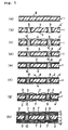
- the through-holes 9 are formed in the same manner as in Example 3 and the resin filler 10 having the same composition as in Example 3 is filled in the through-hole 9 without the formation of the roughened layer (uneven layer) 11 (see Fig. 4 ).
- the formation of the through-hole 9 and the formation of the roughened layer (uneven layer) 11 are carried out in the same manner as in Example 3.
- the thickness of the roughened layer 11 is 10 ⁇ m.
Landscapes
- Engineering & Computer Science (AREA)
- Manufacturing & Machinery (AREA)
- Microelectronics & Electronic Packaging (AREA)
- Production Of Multi-Layered Print Wiring Board (AREA)
- Compositions Of Macromolecular Compounds (AREA)
Claims (5)
- Carte de circuit imprimé assemblée multicouche, dans laquelle une pluralité de couches isolantes interlaminaires (2) et une pluralité de couches conductrices (5, 5') sont stratifiées en alternance sur au moins une surface d'un substrat de câblage (1) ayant un circuit conducteur et un trou traversant (9), et les couches conductrices (5, 5') sont électriquement connectées les unes aux autres par l'intermédiaire d'un trou d'interconnexion (7) formé dans les couches isolantes interlaminaires (2),
dans laquelle une couche rugueuse (11) est formée sur la surface du conducteur dans une paroi intérieure du trou traversant (9),
caractérisée en ce que
une charge de résine sans solvant comprenant une résine époxy de type bisphénol durcie au moyen d'un agent durcisseur imidazole et des particules inorganiques est introduite dans le trou traversant (9) formé dans le substrat (1). - Carte de circuit imprimé assemblée multicouche selon la revendication 1, dans laquelle les particules inorganiques sont faites de silice, alumine, mullite, zircone et analogue.
- Carte de circuit imprimé assemblée multicouche selon la revendication 1, dans laquelle les particules inorganiques ont une granulométrie moyenne de 0,1 à 5,0 µm.
- Carte de circuit imprimé assemblée multicouche selon la revendication 3, dans laquelle la taille maximale
des particules inorganiques n'est pas supérieure à l'épaisseur de la couche conductrice. - Carte de circuit imprimé assemblée multicouche selon la revendication 4, dans laquelle la taille maximale des particules inorganiques n'est pas supérieure à l'épaisseur de la couche conductrice de 15 µm.
Applications Claiming Priority (5)
| Application Number | Priority Date | Filing Date | Title |
|---|---|---|---|
| JP27392895 | 1995-10-23 | ||
| JP31746995 | 1995-11-10 | ||
| JP16340296 | 1996-06-24 | ||
| EP96935417A EP0800336B1 (fr) | 1995-10-23 | 1996-10-23 | Resine de remplissage et carte de circuits imprimes multicouche |
| EP04011285A EP1445996B1 (fr) | 1995-10-23 | 1996-10-23 | Panneau à circuit imprimé multicouche édifié |
Related Parent Applications (3)
| Application Number | Title | Priority Date | Filing Date |
|---|---|---|---|
| EP04011285A Division EP1445996B1 (fr) | 1995-10-23 | 1996-10-23 | Panneau à circuit imprimé multicouche édifié |
| EP96935417.4 Division | 1997-05-01 | ||
| EP04011285.6 Division | 2004-05-12 |
Publications (3)
| Publication Number | Publication Date |
|---|---|
| EP1705973A2 EP1705973A2 (fr) | 2006-09-27 |
| EP1705973A3 EP1705973A3 (fr) | 2009-01-21 |
| EP1705973B1 true EP1705973B1 (fr) | 2011-05-11 |
Family
ID=27322157
Family Applications (4)
| Application Number | Title | Priority Date | Filing Date |
|---|---|---|---|
| EP96935417A Expired - Lifetime EP0800336B1 (fr) | 1995-10-23 | 1996-10-23 | Resine de remplissage et carte de circuits imprimes multicouche |
| EP04011285A Expired - Lifetime EP1445996B1 (fr) | 1995-10-23 | 1996-10-23 | Panneau à circuit imprimé multicouche édifié |
| EP06014607A Expired - Lifetime EP1705973B1 (fr) | 1995-10-23 | 1996-10-23 | Carte de circuit imprimé multicouche avec des couches d'accumulation |
| EP03004268A Expired - Lifetime EP1318708B1 (fr) | 1995-10-23 | 1996-10-23 | Résine de remplissage et panneau à circuit imprimé |
Family Applications Before (2)
| Application Number | Title | Priority Date | Filing Date |
|---|---|---|---|
| EP96935417A Expired - Lifetime EP0800336B1 (fr) | 1995-10-23 | 1996-10-23 | Resine de remplissage et carte de circuits imprimes multicouche |
| EP04011285A Expired - Lifetime EP1445996B1 (fr) | 1995-10-23 | 1996-10-23 | Panneau à circuit imprimé multicouche édifié |
Family Applications After (1)
| Application Number | Title | Priority Date | Filing Date |
|---|---|---|---|
| EP03004268A Expired - Lifetime EP1318708B1 (fr) | 1995-10-23 | 1996-10-23 | Résine de remplissage et panneau à circuit imprimé |
Country Status (7)
| Country | Link |
|---|---|
| EP (4) | EP0800336B1 (fr) |
| KR (1) | KR100272850B1 (fr) |
| CN (1) | CN1090891C (fr) |
| DE (3) | DE69633381T2 (fr) |
| MY (1) | MY116680A (fr) |
| SG (1) | SG71684A1 (fr) |
| WO (1) | WO1997016056A1 (fr) |
Families Citing this family (25)
| Publication number | Priority date | Publication date | Assignee | Title |
|---|---|---|---|---|
| USRE40947E1 (en) * | 1997-10-14 | 2009-10-27 | Ibiden Co., Ltd. | Multilayer printed wiring board and its manufacturing method, and resin composition for filling through-hole |
| KR100855529B1 (ko) | 1998-09-03 | 2008-09-01 | 이비덴 가부시키가이샤 | 다층프린트배선판 및 그 제조방법 |
| MY144503A (en) | 1998-09-14 | 2011-09-30 | Ibiden Co Ltd | Printed circuit board and method for its production |
| WO2000018202A1 (fr) | 1998-09-17 | 2000-03-30 | Ibiden Co., Ltd. | Tableau de connexions multicouche d'accumulation |
| SE9803670L (sv) * | 1998-10-26 | 2000-04-27 | Ericsson Telefon Ab L M | Förfarande vid framställning av kretskort |
| JP2000261147A (ja) * | 1999-03-10 | 2000-09-22 | Shinko Electric Ind Co Ltd | 多層配線基板及びその製造方法 |
| JP4442832B2 (ja) * | 1999-04-13 | 2010-03-31 | イビデン株式会社 | 多層プリント配線板 |
| EP2086299A1 (fr) | 1999-06-02 | 2009-08-05 | Ibiden Co., Ltd. | Carte de circuit imprimé multicouches et procédé de fabrication d'une carte de circuit imprimé multicouches |
| CN1199536C (zh) | 1999-10-26 | 2005-04-27 | 伊比登株式会社 | 多层印刷配线板及多层印刷配线板的制造方法 |
| WO2004010751A1 (fr) | 2002-07-18 | 2004-01-29 | Hitachi Chemical Co., Ltd. | Panneau de cablage multicouche, procede permettant de produire ce panneau, dispositif semi-conducteur et dispositif radio-electronique |
| ES2217952B1 (es) * | 2002-12-30 | 2006-03-16 | Lear Automotive (Eeds) Spain, S.L. | Procedimiento para la fabricacion de placas de circuito impreso con espacios entre pistas protegidos. |
| DE10328857B3 (de) * | 2003-06-26 | 2005-03-17 | OCé PRINTING SYSTEMS GMBH | Hülse zum Transport eines Tonergemischs und Verfahren zum Herstellen einer solchen Hülse |
| CN101014890B (zh) * | 2004-09-08 | 2011-01-19 | 东丽株式会社 | 光布线用树脂组合物和光电复合布线基板 |
| CN100591193C (zh) * | 2005-07-15 | 2010-02-17 | 松下电器产业株式会社 | 布线基板、布线材料、覆铜层压板以及布线基板的制造方法 |
| JP5344394B2 (ja) * | 2008-07-10 | 2013-11-20 | 山栄化学株式会社 | 硬化性樹脂組成物、並びにハロゲンフリー樹脂基板及びハロゲンフリービルドアッププリント配線板 |
| TWI517268B (zh) * | 2009-08-07 | 2016-01-11 | 半導體能源研究所股份有限公司 | 端子構造的製造方法和電子裝置的製造方法 |
| JP5077324B2 (ja) * | 2009-10-26 | 2012-11-21 | 株式会社デンソー | 配線基板 |
| CN101720167B (zh) * | 2009-11-20 | 2012-06-06 | 深圳崇达多层线路板有限公司 | 内层芯板树脂塞孔的线路板制作方法 |
| CN101854778B (zh) * | 2010-04-30 | 2011-10-26 | 深圳崇达多层线路板有限公司 | 一种对线路板导电孔进行树脂塞孔的制造工艺 |
| CN102510668B (zh) * | 2011-11-08 | 2014-02-19 | 深圳市景旺电子股份有限公司 | 一种超厚铜pcb板制作方法及其电路板 |
| CN102548199A (zh) * | 2011-12-29 | 2012-07-04 | 广东生益科技股份有限公司 | 电路基板及其制作方法 |
| CN105704915A (zh) * | 2016-04-26 | 2016-06-22 | 浪潮电子信息产业股份有限公司 | 一种耐腐蚀的服务器pcb |
| CN106304665A (zh) * | 2016-08-30 | 2017-01-04 | 江门全合精密电子有限公司 | 10安士铜印刷电路板的制作方法 |
| TWI788471B (zh) * | 2018-01-16 | 2023-01-01 | 日商太陽油墨製造股份有限公司 | 熱硬化性樹脂組成物、其硬化物及印刷配線板 |
| CN117690902B (zh) * | 2024-02-03 | 2024-04-12 | 江门市和美精艺电子有限公司 | 一种含改性胶膜的封装基板 |
Family Cites Families (14)
| Publication number | Priority date | Publication date | Assignee | Title |
|---|---|---|---|---|
| FR2042059A5 (fr) * | 1969-04-02 | 1971-02-05 | Ibm | |
| US3953664A (en) * | 1973-10-26 | 1976-04-27 | Matsushita Electric, Wireless Research Laboratory | Printed circuit board |
| US4555532A (en) * | 1983-10-14 | 1985-11-26 | Hitachi, Ltd. | Epoxy resin composition |
| DE3913966B4 (de) * | 1988-04-28 | 2005-06-02 | Ibiden Co., Ltd., Ogaki | Klebstoffdispersion zum stromlosen Plattieren, sowie Verwendung zur Herstellung einer gedruckten Schaltung |
| US5120384A (en) * | 1989-05-25 | 1992-06-09 | Matsushita Electric Works, Ltd. | Method of manufacturing multilayer laminate |
| EP0453785A1 (fr) * | 1990-04-24 | 1991-10-30 | Oerlikon Contraves AG | Procédé de fabrication d'un circuit à couche mince multicouche à résistances intégrées à couche mince |
| JP3057766B2 (ja) * | 1990-12-18 | 2000-07-04 | 日本ケミコン株式会社 | 厚膜多層回路基板及びその製造方法 |
| JPH04221886A (ja) * | 1990-12-21 | 1992-08-12 | Nippon Chemicon Corp | 厚膜多層回路基板及びその製造方法 |
| JP2778323B2 (ja) * | 1992-01-23 | 1998-07-23 | 株式会社日立製作所 | プリント配線基板およびその製造方法 |
| JP3053970B2 (ja) * | 1992-07-27 | 2000-06-19 | 住友ベークライト株式会社 | 多層印刷配線板の製造方法 |
| US5766670A (en) * | 1993-11-17 | 1998-06-16 | Ibm | Via fill compositions for direct attach of devices and methods for applying same |
| US5450290A (en) * | 1993-02-01 | 1995-09-12 | International Business Machines Corporation | Printed circuit board with aligned connections and method of making same |
| JPH06275959A (ja) * | 1993-03-22 | 1994-09-30 | Hitachi Ltd | 多層配線基板とその製造方法および両面プリント配線板の製造方法 |
| GB2283617A (en) * | 1993-11-02 | 1995-05-10 | Coates Brothers Plc | Blocking through-holes in laminar substrates |
-
1996
- 1996-10-23 EP EP96935417A patent/EP0800336B1/fr not_active Expired - Lifetime
- 1996-10-23 DE DE69633381T patent/DE69633381T2/de not_active Expired - Lifetime
- 1996-10-23 WO PCT/JP1996/003088 patent/WO1997016056A1/fr not_active Ceased
- 1996-10-23 DE DE69633690T patent/DE69633690T2/de not_active Expired - Lifetime
- 1996-10-23 EP EP04011285A patent/EP1445996B1/fr not_active Expired - Lifetime
- 1996-10-23 KR KR1019970704312A patent/KR100272850B1/ko not_active Expired - Fee Related
- 1996-10-23 EP EP06014607A patent/EP1705973B1/fr not_active Expired - Lifetime
- 1996-10-23 SG SG1996010945A patent/SG71684A1/en unknown
- 1996-10-23 EP EP03004268A patent/EP1318708B1/fr not_active Expired - Lifetime
- 1996-10-23 CN CN96191555A patent/CN1090891C/zh not_active Expired - Lifetime
- 1996-10-23 MY MYPI96004387A patent/MY116680A/en unknown
- 1996-10-23 DE DE69637655T patent/DE69637655D1/de not_active Expired - Lifetime
Also Published As
| Publication number | Publication date |
|---|---|
| EP0800336A1 (fr) | 1997-10-08 |
| EP1318708A3 (fr) | 2003-06-18 |
| DE69633690T2 (de) | 2005-03-10 |
| EP1445996A3 (fr) | 2004-08-18 |
| DE69633381D1 (de) | 2004-10-21 |
| SG71684A1 (en) | 2000-04-18 |
| EP1318708A2 (fr) | 2003-06-11 |
| KR987001202A (ko) | 1998-04-30 |
| EP1445996A2 (fr) | 2004-08-11 |
| MY116680A (en) | 2004-03-31 |
| EP1445996B1 (fr) | 2008-08-20 |
| DE69633381T2 (de) | 2005-02-24 |
| WO1997016056A1 (fr) | 1997-05-01 |
| CN1169234A (zh) | 1997-12-31 |
| CN1090891C (zh) | 2002-09-11 |
| EP0800336B1 (fr) | 2004-09-15 |
| DE69637655D1 (de) | 2008-10-02 |
| EP1318708B1 (fr) | 2004-10-20 |
| KR100272850B1 (ko) | 2001-01-15 |
| EP1705973A2 (fr) | 2006-09-27 |
| EP0800336A4 (fr) | 1999-04-21 |
| EP1705973A3 (fr) | 2009-01-21 |
| DE69633690D1 (de) | 2004-11-25 |
Similar Documents
| Publication | Publication Date | Title |
|---|---|---|
| EP1705973B1 (fr) | Carte de circuit imprimé multicouche avec des couches d'accumulation | |
| US6010768A (en) | Multilayer printed circuit board, method of producing multilayer printed circuit board and resin filler | |
| EP1893005B1 (fr) | Panneau à circuit imprimé et procédé de fabrication d'un panneau à circuit imprimé | |
| EP0952762B1 (fr) | Carte a circuit imprime et son procede de fabrication | |
| EP1667506B1 (fr) | Procédé de placage anélectrolytique et plaquette de circuit imprimé | |
| US6248428B1 (en) | Adhesive for electroless plating, raw material composition for preparing adhesive for electroless plating and printed wiring board | |
| EP1005261B1 (fr) | Adhesif utile pour effectuer le depot autocatalytique, composition de produit de depart utile pour preparer de l'adhesif pour depot catalytique et carte imprimee | |
| JPH10256724A (ja) | 多層プリント配線板 | |
| JP2001203448A (ja) | 多層プリント配線板およびその製造方法 | |
| JPH10247783A (ja) | 多層プリント配線板およびその製造方法 | |
| JPH10247784A (ja) | 多層プリント配線板およびその製造方法 | |
| JPH10200265A (ja) | 多層プリント配線板 | |
| JP3098729B2 (ja) | 多層プリント配線板の製造方法 | |
| JP2000156551A (ja) | プリント配線板、被処理体及びプリント配線板の製造方法 | |
| JPH10242639A (ja) | 多層プリント配線板およびその製造方法 | |
| JP3995794B2 (ja) | 無電解めっき用接着剤およびプリント配線板 | |
| JP2000077846A (ja) | プリント配線板の製造方法 | |
| JP4215872B2 (ja) | 多層プリント配線板、被処理体及び多層プリント配線板の製造方法 | |
| JP2000059006A (ja) | プリント配線板の製造方法 | |
| JPH11284337A (ja) | 多層プリント配線板の製造方法 | |
| JP2000294932A (ja) | 多層プリント配線板の製造方法 | |
| JP2000183521A (ja) | プリント配線板、被処理体及びプリント配線板の製造方法 | |
| JP2000082871A (ja) | プリント配線板及びその製造方法 | |
| JP2000077827A (ja) | プリント配線板 | |
| JPH10242640A (ja) | プリント配線板 |
Legal Events
| Date | Code | Title | Description |
|---|---|---|---|
| PUAI | Public reference made under article 153(3) epc to a published international application that has entered the european phase |
Free format text: ORIGINAL CODE: 0009012 |
|
| 17P | Request for examination filed |
Effective date: 20060713 |
|
| AC | Divisional application: reference to earlier application |
Ref document number: 1445996 Country of ref document: EP Kind code of ref document: P Ref document number: 0800336 Country of ref document: EP Kind code of ref document: P |
|
| AK | Designated contracting states |
Kind code of ref document: A2 Designated state(s): DE FI GB NL |
|
| PUAL | Search report despatched |
Free format text: ORIGINAL CODE: 0009013 |
|
| AK | Designated contracting states |
Kind code of ref document: A3 Designated state(s): DE FI GB NL |
|
| AKX | Designation fees paid |
Designated state(s): DE FI GB NL |
|
| 17Q | First examination report despatched |
Effective date: 20100408 |
|
| GRAP | Despatch of communication of intention to grant a patent |
Free format text: ORIGINAL CODE: EPIDOSNIGR1 |
|
| GRAS | Grant fee paid |
Free format text: ORIGINAL CODE: EPIDOSNIGR3 |
|
| GRAA | (expected) grant |
Free format text: ORIGINAL CODE: 0009210 |
|
| AC | Divisional application: reference to earlier application |
Ref document number: 1445996 Country of ref document: EP Kind code of ref document: P Ref document number: 0800336 Country of ref document: EP Kind code of ref document: P |
|
| AK | Designated contracting states |
Kind code of ref document: B1 Designated state(s): DE FI GB NL |
|
| REG | Reference to a national code |
Ref country code: GB Ref legal event code: FG4D |
|
| REG | Reference to a national code |
Ref country code: DE Ref legal event code: R096 Ref document number: 69638376 Country of ref document: DE Effective date: 20110622 |
|
| REG | Reference to a national code |
Ref country code: NL Ref legal event code: VDEP Effective date: 20110511 |
|
| PG25 | Lapsed in a contracting state [announced via postgrant information from national office to epo] |
Ref country code: FI Free format text: LAPSE BECAUSE OF FAILURE TO SUBMIT A TRANSLATION OF THE DESCRIPTION OR TO PAY THE FEE WITHIN THE PRESCRIBED TIME-LIMIT Effective date: 20110511 |
|
| PG25 | Lapsed in a contracting state [announced via postgrant information from national office to epo] |
Ref country code: NL Free format text: LAPSE BECAUSE OF FAILURE TO SUBMIT A TRANSLATION OF THE DESCRIPTION OR TO PAY THE FEE WITHIN THE PRESCRIBED TIME-LIMIT Effective date: 20110511 |
|
| PLBE | No opposition filed within time limit |
Free format text: ORIGINAL CODE: 0009261 |
|
| STAA | Information on the status of an ep patent application or granted ep patent |
Free format text: STATUS: NO OPPOSITION FILED WITHIN TIME LIMIT |
|
| 26N | No opposition filed |
Effective date: 20120214 |
|
| REG | Reference to a national code |
Ref country code: DE Ref legal event code: R097 Ref document number: 69638376 Country of ref document: DE Effective date: 20120214 |
|
| GBPC | Gb: european patent ceased through non-payment of renewal fee |
Effective date: 20111023 |
|
| PG25 | Lapsed in a contracting state [announced via postgrant information from national office to epo] |
Ref country code: GB Free format text: LAPSE BECAUSE OF NON-PAYMENT OF DUE FEES Effective date: 20111023 |
|
| PGFP | Annual fee paid to national office [announced via postgrant information from national office to epo] |
Ref country code: DE Payment date: 20151020 Year of fee payment: 20 |
|
| REG | Reference to a national code |
Ref country code: DE Ref legal event code: R071 Ref document number: 69638376 Country of ref document: DE |