EP1708166A2 - Chip-on-Glass-Flüssigkristallanzeige und Datenübertragungsverfahren dafür - Google Patents
Chip-on-Glass-Flüssigkristallanzeige und Datenübertragungsverfahren dafür Download PDFInfo
- Publication number
- EP1708166A2 EP1708166A2 EP06002941A EP06002941A EP1708166A2 EP 1708166 A2 EP1708166 A2 EP 1708166A2 EP 06002941 A EP06002941 A EP 06002941A EP 06002941 A EP06002941 A EP 06002941A EP 1708166 A2 EP1708166 A2 EP 1708166A2
- Authority
- EP
- European Patent Office
- Prior art keywords
- control signal
- source driver
- image data
- source
- transceiver
- Prior art date
- Legal status (The legal status is an assumption and is not a legal conclusion. Google has not performed a legal analysis and makes no representation as to the accuracy of the status listed.)
- Granted
Links
- 239000011521 glass Substances 0.000 title claims abstract description 22
- 239000004973 liquid crystal related substance Substances 0.000 title claims abstract description 14
- 230000005540 biological transmission Effects 0.000 title claims description 26
- 238000000034 method Methods 0.000 title claims description 19
- 239000000758 substrate Substances 0.000 claims abstract description 12
- 230000001934 delay Effects 0.000 claims abstract description 8
- 238000005516 engineering process Methods 0.000 claims abstract description 5
- 238000010586 diagram Methods 0.000 description 20
- 238000004519 manufacturing process Methods 0.000 description 6
- 238000005070 sampling Methods 0.000 description 5
- 239000003999 initiator Substances 0.000 description 4
- 230000010287 polarization Effects 0.000 description 4
- 230000004048 modification Effects 0.000 description 3
- 238000012986 modification Methods 0.000 description 3
- 230000008901 benefit Effects 0.000 description 2
- 230000008878 coupling Effects 0.000 description 2
- 238000010168 coupling process Methods 0.000 description 2
- 238000005859 coupling reaction Methods 0.000 description 2
- 230000003071 parasitic effect Effects 0.000 description 2
- 230000004044 response Effects 0.000 description 2
- ZLGYJAIAVPVCNF-UHFFFAOYSA-N 1,2,4-trichloro-5-(3,5-dichlorophenyl)benzene Chemical compound ClC1=CC(Cl)=CC(C=2C(=CC(Cl)=C(Cl)C=2)Cl)=C1 ZLGYJAIAVPVCNF-UHFFFAOYSA-N 0.000 description 1
- 230000003111 delayed effect Effects 0.000 description 1
- 230000005855 radiation Effects 0.000 description 1
Images


Classifications
-
- G—PHYSICS
- G09—EDUCATION; CRYPTOGRAPHY; DISPLAY; ADVERTISING; SEALS
- G09G—ARRANGEMENTS OR CIRCUITS FOR CONTROL OF INDICATING DEVICES USING STATIC MEANS TO PRESENT VARIABLE INFORMATION
- G09G3/00—Control arrangements or circuits, of interest only in connection with visual indicators other than cathode-ray tubes
- G09G3/20—Control arrangements or circuits, of interest only in connection with visual indicators other than cathode-ray tubes for presentation of an assembly of a number of characters, e.g. a page, by composing the assembly by combination of individual elements arranged in a matrix no fixed position being assigned to or needed to be assigned to the individual characters or partial characters
- G09G3/34—Control arrangements or circuits, of interest only in connection with visual indicators other than cathode-ray tubes for presentation of an assembly of a number of characters, e.g. a page, by composing the assembly by combination of individual elements arranged in a matrix no fixed position being assigned to or needed to be assigned to the individual characters or partial characters by control of light from an independent source
- G09G3/36—Control arrangements or circuits, of interest only in connection with visual indicators other than cathode-ray tubes for presentation of an assembly of a number of characters, e.g. a page, by composing the assembly by combination of individual elements arranged in a matrix no fixed position being assigned to or needed to be assigned to the individual characters or partial characters by control of light from an independent source using liquid crystals
- G09G3/3611—Control of matrices with row and column drivers
- G09G3/3685—Details of drivers for data electrodes
- G09G3/3688—Details of drivers for data electrodes suitable for active matrices only
-
- G—PHYSICS
- G09—EDUCATION; CRYPTOGRAPHY; DISPLAY; ADVERTISING; SEALS
- G09G—ARRANGEMENTS OR CIRCUITS FOR CONTROL OF INDICATING DEVICES USING STATIC MEANS TO PRESENT VARIABLE INFORMATION
- G09G3/00—Control arrangements or circuits, of interest only in connection with visual indicators other than cathode-ray tubes
- G09G3/20—Control arrangements or circuits, of interest only in connection with visual indicators other than cathode-ray tubes for presentation of an assembly of a number of characters, e.g. a page, by composing the assembly by combination of individual elements arranged in a matrix no fixed position being assigned to or needed to be assigned to the individual characters or partial characters
- G09G3/34—Control arrangements or circuits, of interest only in connection with visual indicators other than cathode-ray tubes for presentation of an assembly of a number of characters, e.g. a page, by composing the assembly by combination of individual elements arranged in a matrix no fixed position being assigned to or needed to be assigned to the individual characters or partial characters by control of light from an independent source
- G09G3/36—Control arrangements or circuits, of interest only in connection with visual indicators other than cathode-ray tubes for presentation of an assembly of a number of characters, e.g. a page, by composing the assembly by combination of individual elements arranged in a matrix no fixed position being assigned to or needed to be assigned to the individual characters or partial characters by control of light from an independent source using liquid crystals
- G09G3/3611—Control of matrices with row and column drivers
- G09G3/3648—Control of matrices with row and column drivers using an active matrix
- G09G3/3666—Control of matrices with row and column drivers using an active matrix with the matrix divided into sections
-
- G—PHYSICS
- G09—EDUCATION; CRYPTOGRAPHY; DISPLAY; ADVERTISING; SEALS
- G09G—ARRANGEMENTS OR CIRCUITS FOR CONTROL OF INDICATING DEVICES USING STATIC MEANS TO PRESENT VARIABLE INFORMATION
- G09G2300/00—Aspects of the constitution of display devices
- G09G2300/04—Structural and physical details of display devices
- G09G2300/0404—Matrix technologies
- G09G2300/0408—Integration of the drivers onto the display substrate
-
- G—PHYSICS
- G09—EDUCATION; CRYPTOGRAPHY; DISPLAY; ADVERTISING; SEALS
- G09G—ARRANGEMENTS OR CIRCUITS FOR CONTROL OF INDICATING DEVICES USING STATIC MEANS TO PRESENT VARIABLE INFORMATION
- G09G2310/00—Command of the display device
- G09G2310/02—Addressing, scanning or driving the display screen or processing steps related thereto
- G09G2310/0264—Details of driving circuits
- G09G2310/027—Details of drivers for data electrodes, the drivers handling digital grey scale data, e.g. use of D/A converters
-
- G—PHYSICS
- G09—EDUCATION; CRYPTOGRAPHY; DISPLAY; ADVERTISING; SEALS
- G09G—ARRANGEMENTS OR CIRCUITS FOR CONTROL OF INDICATING DEVICES USING STATIC MEANS TO PRESENT VARIABLE INFORMATION
- G09G2310/00—Command of the display device
- G09G2310/02—Addressing, scanning or driving the display screen or processing steps related thereto
- G09G2310/0264—Details of driving circuits
- G09G2310/0281—Arrangement of scan or data electrode driver circuits at the periphery of a panel not inherent to a split matrix structure
-
- G—PHYSICS
- G09—EDUCATION; CRYPTOGRAPHY; DISPLAY; ADVERTISING; SEALS
- G09G—ARRANGEMENTS OR CIRCUITS FOR CONTROL OF INDICATING DEVICES USING STATIC MEANS TO PRESENT VARIABLE INFORMATION
- G09G2310/00—Command of the display device
- G09G2310/04—Partial updating of the display screen
-
- G—PHYSICS
- G09—EDUCATION; CRYPTOGRAPHY; DISPLAY; ADVERTISING; SEALS
- G09G—ARRANGEMENTS OR CIRCUITS FOR CONTROL OF INDICATING DEVICES USING STATIC MEANS TO PRESENT VARIABLE INFORMATION
- G09G2330/00—Aspects of power supply; Aspects of display protection and defect management
- G09G2330/02—Details of power systems and of start or stop of display operation
- G09G2330/021—Power management, e.g. power saving
-
- G—PHYSICS
- G09—EDUCATION; CRYPTOGRAPHY; DISPLAY; ADVERTISING; SEALS
- G09G—ARRANGEMENTS OR CIRCUITS FOR CONTROL OF INDICATING DEVICES USING STATIC MEANS TO PRESENT VARIABLE INFORMATION
- G09G2370/00—Aspects of data communication
- G09G2370/04—Exchange of auxiliary data, i.e. other than image data, between monitor and graphics controller
- G09G2370/045—Exchange of auxiliary data, i.e. other than image data, between monitor and graphics controller using multiple communication channels, e.g. parallel and serial
-
- G—PHYSICS
- G09—EDUCATION; CRYPTOGRAPHY; DISPLAY; ADVERTISING; SEALS
- G09G—ARRANGEMENTS OR CIRCUITS FOR CONTROL OF INDICATING DEVICES USING STATIC MEANS TO PRESENT VARIABLE INFORMATION
- G09G2370/00—Aspects of data communication
- G09G2370/08—Details of image data interface between the display device controller and the data line driver circuit
-
- G—PHYSICS
- G09—EDUCATION; CRYPTOGRAPHY; DISPLAY; ADVERTISING; SEALS
- G09G—ARRANGEMENTS OR CIRCUITS FOR CONTROL OF INDICATING DEVICES USING STATIC MEANS TO PRESENT VARIABLE INFORMATION
- G09G3/00—Control arrangements or circuits, of interest only in connection with visual indicators other than cathode-ray tubes
- G09G3/20—Control arrangements or circuits, of interest only in connection with visual indicators other than cathode-ray tubes for presentation of an assembly of a number of characters, e.g. a page, by composing the assembly by combination of individual elements arranged in a matrix no fixed position being assigned to or needed to be assigned to the individual characters or partial characters
- G09G3/2092—Details of a display terminals using a flat panel, the details relating to the control arrangement of the display terminal and to the interfaces thereto
- G09G3/2096—Details of the interface to the display terminal specific for a flat panel
-
- G—PHYSICS
- G09—EDUCATION; CRYPTOGRAPHY; DISPLAY; ADVERTISING; SEALS
- G09G—ARRANGEMENTS OR CIRCUITS FOR CONTROL OF INDICATING DEVICES USING STATIC MEANS TO PRESENT VARIABLE INFORMATION
- G09G3/00—Control arrangements or circuits, of interest only in connection with visual indicators other than cathode-ray tubes
- G09G3/20—Control arrangements or circuits, of interest only in connection with visual indicators other than cathode-ray tubes for presentation of an assembly of a number of characters, e.g. a page, by composing the assembly by combination of individual elements arranged in a matrix no fixed position being assigned to or needed to be assigned to the individual characters or partial characters
- G09G3/34—Control arrangements or circuits, of interest only in connection with visual indicators other than cathode-ray tubes for presentation of an assembly of a number of characters, e.g. a page, by composing the assembly by combination of individual elements arranged in a matrix no fixed position being assigned to or needed to be assigned to the individual characters or partial characters by control of light from an independent source
- G09G3/36—Control arrangements or circuits, of interest only in connection with visual indicators other than cathode-ray tubes for presentation of an assembly of a number of characters, e.g. a page, by composing the assembly by combination of individual elements arranged in a matrix no fixed position being assigned to or needed to be assigned to the individual characters or partial characters by control of light from an independent source using liquid crystals
- G09G3/3611—Control of matrices with row and column drivers
- G09G3/3674—Details of drivers for scan electrodes
- G09G3/3677—Details of drivers for scan electrodes suitable for active matrices only
Definitions
- the invention relates in general to the liquid crystal display, and more particularly to the chip-on-glass liquid crystal display.
- LCD Liquid crystal displays
- the LCD includes a timing controller, source drivers and at least one gate driver to drive its liquid crystal panel.
- the timing controller is welded on a control print circuit board
- the source drivers are welded on a X-board
- the gate driver is welded on a Y-board conventionally.
- the control print circuit board connects to the X-board via flexible printed circuit boards (FPCs), while the X-board and the Y board each connects to the liquid crystal panel via other FPCs. Therefore, the conventional LCD requires at least three boards to be connected to the panel and the manufacturing process is thus complex.
- the chip-one-glass (COG) LCD has been developed.
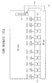
- FIG. 1 is diagram of a conventional COG LCD.
- the COG LCD 100 includes a panel 110, a plurality of source drivers 112, at least one gate driver 114, a printed circuit board 120 and a plurality of flexible printed circuit board 130.
- the source drivers 112 and the gate driver 114 are disposed on the glass substrate of the panel 110 and electrically connects to the printed circuit board 120 via the flexible printed circuit boards 130.
- the timing controller (not shown in FIG. 1) is disposed on the printed circuit board 120, outputs image data and the control signal to the source drivers 112 and the gate driver 114.
- PCB 120 only one board (PCB 120), instead of three, is required to connect to the panel 110 via the FPCs 130, therefore, the manufacturing process is simplified.
- the manufacturing process of COG LCD is still not simplified enough because a plurality of the flexible printed circuit boards are needed, and in the above example in FIG. 1, the number of the flexible printed circuit board is 11. Besides, the flexible printed boards need a plurality of contact points with the liquid crystal panel and the possibility of electrical contact failure is thus increased.
- the invention achieves the above-identified objects by providing a new liquid crystal display (LCD) comprising a glass substrate, a plurality of serial-connected source drivers and at least one gate driver, disposed on the glass substrate by chip-on-glass technology, a timing controller for generating image data and a control signal, and at least one flexible printed circuit board.
- the flexible printed circuit board receives the image data and the control signal for transmitting to the corresponding source driver. Then the corresponding source driver transmits the image data and the control signal to the neighboring source drivers such that all the source drivers respectively get the image data and the control signal.
- the flexible printed circuit board is disposed such that delays and distortions of the image data and the control signal are acceptable to the source drivers.
- FIG. 1 is diagram of a conventional COG LCD.
- FIG. 2A is a diagram of a chip-on-glass (COG) liquid crystal display (LCD) according to a preferred embodiment of the invention.
- COG chip-on-glass
- LCD liquid crystal display
- FIG. 2B is a diagram of a COG LCD according to another preferred embodiment of the invention.
- FIG. 3 is a diagram of control signals of the source drivers and the gate drivers of the LCD.
- FIG. 4 is a format diagram of a control packet.
- FIG. 5A is a diagram of the source driver according to the preferred embodiment of the invention.
- FIG. 5B is a block diagram of the wave generator in FIG. 5A.
- FIG. 5C is a block diagram of the ID recognizer in FIG. 5B.
- FIG. 5D is a waveform diagram of control signal POL.
- FIG. 5E is a waveform diagram of the generation of the control signal TP.
- FIG. 6A is a flowchart of a convergent transmission method for power saving.
- FIG. 6B is a flowchart of a divergent transmission method for power saving.
- FIG. 2A is a diagram of a chip-on-glass (COG) liquid crystal display (LCD) according to a preferred embodiment of the invention.
- the LCD 200 includes a panel 210, a plurality of source drivers (S/D) 212(1)-212(10), at least one gate driver 214, a printed circuit board 220 and flexible printed circuit board (FPC) 230 and 232.
- the source drivers 212 and gate driver 214 are disposed on the glass substrate of the panel 210 by the chip-on-glass technology.
- the timing controller 225 is disposed on the printed circuit board 220 for outputting image data and control signals both to source drivers 212(3) and 212(8) respectively via the flexible printed circuit boards 230 and 232.
- the source driver 212(3) transmits the image data and the control signals to the neighboring source drivers 212(1), 212(2), 212(4) and 212(5)
- the source driver 212(8) transmits the image data and the control signals to the neighboring source drivers 212(5), 212(6), 212(7), 212(8) and 212(10).
- one of the source drivers such as the source driver 212(1), which is nearest to the gate driver 214, can generate gate control signals G to the gate driver 214.
- the reason to choose the source driver nearest to the gate driver 212 is to reduce the length of the wire therebetween so as to effectively reduce the distortions and delays of the gate control signals G.
- source drives can also be used to generate the gate control signals G, not just limited to the source driver 212(1).
- the number of the flexible printed circuit boards are greatly reduced to 2 because the LCD uses the wires disposed on the glass substrate for transmitting the image data and the control signals.
- the source drivers 212 each has a first operation mode and a second operation mode.
- the source driver 212(3) and the source driver 212(8) are set to the first operation mode to execute the dual-way transmission. That is, the source driver 212(3) and the source driver 212(8) each receives the image data and control signals from the timing controller 225 and transmits them to the neighboring source drivers at both the right side and the left side thereof. Take the source driver 212(3) for example, the source driver 212(3) can simultaneously transmit the image data and control signals to both the neighboring source driver 212(2) and 212(4), which are located at the two sides of the source driver 212(3).
- the source drivers 212(1), 212(2), 212(4)-212(7), 212(9) and 212(10) are set to the second operation mode to execute the single-way transmission, and are not directly connected to the timing controller 225. That is, the source drivers 212(1), 212(2), 212(4)-212(7), 212(9) and 212(10) each can receive the image data and the control signals from the right (or left) source driver and transmit them to the left (or right) source driver. Take the source driver 212(2) for example, it receives the image data and the control signals from the source driver 212(3) at right side thereof and transmits them to the source driver 212(1) at the left side thereof.
- the LCD 200 is a big screen monitor having 10 source drivers and two flexible printed circuit board 230 and 232. The number of flexible printed circuit boards is not limited to two as long as the distortions and delays of signals is acceptable.
- the source drivers are divided into a left group including source drivers 212(1)-212(5) and a right group including source drivers 212(6)-212(10).
- the flexible printed circuit boards 230 connects to the center source drivers 212(3) of the left group, and the flexible printed circuit boards 232 connects to the center source drivers 212(8) of the right group, such that the distortions and delays of signals, caused by the parasitic capacitance and resistance, can be minimized.
- the source drivers can also be divided into more than three groups and each group directly connects to the timing controller via a flexible printed circuit board, so long as the distortions and delays of the signals are acceptable.
- FIG. 2B is a diagram of a COG LCD 250 according to another preferred embodiment of the invention.
- the LCD 250 further includes a gate driver 216 at the right side of the panel 210.
- the gate driver 214 and 216 together drivers the panel 210 from two sides thereof.
- the other elements of LCD 250 is the same with that of the LCD 200 and are not described here again.
- FIG. 3 is a diagram of control signals of the source drivers and the gate drivers of the LCD.
- the control signals includes gate control signals G and source control signals S.
- the gate control signals G includes a gate driver start signal STV for representing the start of a frame, a gate clock signal CPV for enabling a gate line, and a gate driver output enable signal OEV for defining the enabled duration of the gate line.
- the source control signals S includes a source driver start signal STH for notifying the source driver to start to prepare the data of a horizontal line, a data enable signal DE for starting to receive data, a load signal TP for starting to output driving voltages to the data lines, and a polarization control signal POL for controlling the polarization inversion.
- the source driver 212 When the source driver start signal STH is asserted, the source driver 212 start to prepare to receive data, and after a period td1, the data enable signal DE is asserted such that the timing controller 225 starts to output the image data to the source drivers 212.
- the source drivers 212 generates the driving voltage with the polarization designated by the polarization control signal POL and then outputs the driving voltages to the panel 210 according to the load signal Tp.
- control signals are outputted by the timing controller directly to each source driver 112 and the gate driver 114.
- Each control signal conventionally needs at least one wire to transmit, and thus a plurality of wires are required. And, the control signals are easily distorted and delayed because the wires between the timing controller and the source drivers and the gate driver have parasitic capacitance and resistance.
- the timing controller 225 integrates the control signals into a control bitstream C and transmits it by a wire to the source drivers 212.
- the control signals can be packed into a plurality of control packets, each representing an event relevant to a control signal.
- the timing controller 225 can designate one source driver 212 to receive the control packet by a target identification.
- the target identification is, for example, included in the control packet for each source driver to identify.
- the source driver 212 can decode the control packet to generate the control signal. Therefore, the number of the wires required to transmit the control signals is thus greatly reduced in the embodiment.
- the source driver 212 has a built-in identification so as to identify whether the received control packet is for its own by comparing the target identification of the control packet with the built-in identification.
- control signals are each transmitted by a wire from the timing controller to the source driver/gate driver.
- the source drivers and the gate driver each needs a plurality of control signals and thus the number of the wires for transmitting the control signals is great. Therefore number of wires in the conventional flexible printed circuit board is also great, so the cost and quality of the conventional flexible printed circuit board is also increased. Besides, the lengths of the wires between the timing controller and the source drivers/gate driver are so long that the delays and distortions of the signals are easily occurred.
- the timing controller 225 transmits the control bitstream C to the source driver only via at least one wire.
- the control bitstream C includes a plurality of control packets, each representing an event of one corresponding control signal, such as a pull high event or a pull low event.
- the source driver 212 After receiving the control packet, the source driver 212 generates the corresponding control signal by pulling high or pulling low accordingly.
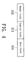
- FIG. 4 is a format diagram of a control packet.
- a control packet includes a header field 310 and a control item, which includes a control field 312 and a data field 314.
- the header field 310 records a predetermined pattern for identifying the start of a packet, the predetermined pattern is 0x11111 for example.
- the control field 312 records the type of the event, such as the STH event, the TP event, the pull high event, the pull low event and the initialization event.
- the data field 314 records the parameters of the event.
- each control packet has 16 bits. If receiving the control packet by dual-edge sampling, it takes 8 clock to read one control packet. That is, the control signal generated by a pull high event and a pull low event must remain at high level for at least a duration of 8 clocks.
- the control signals POL, CPV, STV, OEV can each be generated by a pull high event and a pull low event.
- the control signals that has the duration less than 8 clocks, such as control signals STH and TP are generated respectively by the STH event and the TP event.
- the source driver pulls high the control signal STH/TP for a pre-determined period td2/tw1 and then pulls low the control signal STH/TP. It is worth noticing that the sampling method for receiving the control packet is not limited to dual-edge sampling, rising-edge sampling or falling-edge sampling can also be used.
- the data field 314 thereof records the target identification.
- the source drivers 212(1)-212(10) have the built-in identifications of 0x0001-0x1010, respectively. After receiving the control packet with STH event, the source driver compares the target identification of this control packet with the built-in identification, pull high the control signal STH if the comparison is matched, and then pull low the control signal STH after a period td2.
- control signals TP and CPV are pulled high at the same time, so after receiving the control packet with TP event, control signals TP and CPV are pulled high.
- the control signal TP is then pulled low after a period tw1, and the control signal CPV is pulled low after receiving the control packet with pull low event of CPV.
- Control signals POL, STV and OEV are generated by a pull high event and a pull low event.
- its data field 314 designates which signal is to be pulled high.
- its data field 314 designates which signal is to be pulled low.
- control packet with the control field 312 recording an initialization event it is for setting several kinds of initialization, such as the fan out of the source drivers. Other kinds of events can also be represented by the control packets and would not be described herein.
- control bitstream C only at least one wire is required to transmit the control bitstream C, so the number of wires connecting the timing controller and the source drivers are greatly reduced, the layout of the circuit is simplified, and the stability is enhanced.
- control bitstream C can integrate only a part of the control signals and leave other part of the control signals to be transmitted respectively in independent wires. Although not all the control signals are integrated to the control bitstream, the number of wires can also be reduced.
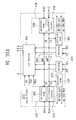
- FIG. 5A is a diagram of the source driver according to the preferred embodiment of the invention.
- the source driver 212 includes a receiver 410, 412, a transceiver 413, 415, a bus switch 422, a wave generator 420, 421, and a driving unit 434.
- the transceiver 413 includes a control transceiver 414 and a data transceiver 424
- the transceiver 415 includes a control transceiver 416 and a data transceiver 426.
- the bus switch 422 includes two switches SW1 and SW2.
- the bus switch turns off the switches SW1 and SW2 such that the control transceiver 414 and 416 are disconnected and the data transceiver 424 and 426 are disconnected.
- the control bitstream C1 and the image data D1 received by the receiver 410 are transmitted to the control transceiver 414 and the data transceiver 424, respectively, and the control bitstream C2 and the image data D2 received by the receiver 410 are transmitted to the control transceiver 416 and the data transceiver 426, respectively.
- the source driver 212(1)-212(2), 212(4)-212(7), 212(9), or 212(10) in this embodiment, operates in the second operation mode
- the receivers 410 and 412 are disabled, and the bus switch turns on the switches SW1 and SW2 such that the transceivers 413 and 415 are connected, that is, the data transceivers 424 and 426 are connected and the control transceivers 414 and 416 are connected.
- the source driver can transmit the control bitstream and the image data received to the next adjacent source driver in response to the designated transmission direction.
- the wave generator 420 and 421 receives the control bitstream C1 and C2 respectively for generating source control signals S, such as STH(1), STH(2), POL(1), POL(2), TP(1) and TP(2), etc., and thus generating the gate control signals G, such as CPV(1), CPV(2), STV(1), STV(2), OEV(1), OEV(2) and etc.
- the control signals G are generated by one of the source drivers.
- one of the source drivers 212 such as 212(1) that is nearest to the gate driver 214, generates the gate control signals G, while the other source drivers 212 do not.
- two source drivers such as 212(1) and 212(10) that are respectively nearest to the gate drivers 214 and 216, generate the gate control signals G respectively for the gate drivers 214 and 216, while others do not.
- the driving unit 434 When receiving the signal STH, the driving unit 434 starts to latch image data D for converting to analog driving voltages in response to the signal POL, and then transmits the analog driving signals to the panel 210 after receiving the load signal TP.
- the wave generators 420 and 421 are both activated to receive the control bitstreams C1 and C2 respectively and generate the source control signals S and the gate control signals G, while the control bitstream C1 and C2 are independent, and image data D1 and D2 are independent.
- the control bitstream C1 is the control bitstream C2
- the image data D1 is the image data D2
- the other wave generator in the second-operation-mode source driver can be disabled, omitted or still activated to generate the source control signals S and the gate control signals G.
- FIG. 5B is a block diagram of the wave generator in FIG. 5A.
- Each of the wave generators 420 and 412 includes a parser 451, an ID recognizer 453, a signal generator 460 and an initiator 470.
- the parser 451 receives the control bitstream C to parse the control item, including the control field 312 and a data field 314, of a control packet, and sends the parsed control item to the ID recognizer 453, the signal generator 460 or the initiator 470 correspondingly: the control item with the identity event, which is the STH event in this embodiment, is sent to the ID recognizer 453; the control item with the pull high event or the pull low event is set to the signal generator 460; the control item with the initialization event is sent to the initiator 470.
- FIG. 5C is a block diagram of the ID recognizer in FIG. 5B.
- the recognizer 453 includes a comparator 456.
- Each source driver has a unique chip identity IDp.
- the chip identity IDp is set externally, for example by, respectively, pulling high or pulling low the pins of the source driver on the glass substrate.
- the comparator 456 triggers the signal STH when the comparison of the chip identity IDp with a target identity IDt extracted from the control packet is matched.
- the duration time td2 of the signal STH can be pre-determined in the comparator 456.
- the signal generator 460 pulls high the corresponding signal after receiving the control item with the pull high event. The level of the pull-high signal is maintained until the signal generator 460 receives the corresponding control item with the pull low event. Take generation of the control signal POL for example.
- FIG. 5D is a waveform diagram of control signal POL.
- the signal generator 460 pulls high the signal PH; when receiving the control with the corresponding pull low event L, the signal generator 460 pulls low the signal PL. Then, the coupling of the signal PH and the signal PL is the signal POL.
- the other control signals such as CPV, STV, OEV, are also generated by the above-mentioned procedure.
- FIG. 5E is a waveform diagram of the generation of the control signal TP.
- the signal generator 460 pulls high the signal TH, then counts for a pre-determined period tw1, and then pulls low the signal TL.
- the coupling of the signal TH and the signal TL is the control signal TP.
- the gate control signals G can also be generated according to the source control signals, such as STH or TP.
- the source control signals such as STH or TP.
- STH source control signals
- FIG. 3 Take the generation of the signal CPV according to the control signal STH for example: when the control signal STH of the source driver 212(1) is asserted, the counter thereof is activated, and the signal CPV is pulled high after a period td6 passed, and, after a period tw4 passed, the signal CPV is pulled low.
- the initiator 470 After receiving the control item with the initialization event, the initiator 470 outputs a DC value to set the corresponding parameter.
- the source driver of the embodiment can reduce the control signal decay because the source control signals is generated by the source driver itself, not by the timing controller conventionally.
- the embodiment can save the number of wires from the timing controller to the gate driver because the source driver can generate the gate control signals and directly send to the gate driver via the wires on the glass substrate.
- the quality of the gate control signals are thus improved because the lengths of the transmission wires are reduced.
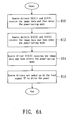
- FIG. 6A is a flowchart of a convergent transmission method for power saving. Take the source drivers 212(1)-212(5) in FIG. 2A for example. First, at step 610, the source drivers 212(1) and 212(5), which have the farthest distances away from the timing controller 225, receive the image data transmitted by the timing controller 225 via the source drivers, and then enter the power-saving mode, which turns of the power for the data transceivers 424 and 426 of the source drivers 212(1) and 212(5), for example.
- the source drivers 212(2) and 212(4) which are the active ones having the farthest distances away from the timing controller 225, receive the image data and then enter the power-saving mode, which turns of the power for the data transceivers 424 and 426 of the source drivers 212(2) and 212(4), for example.
- the source driver 212(3) receives the image data from the timing controller 225 and then enters the power-saving mode. It is noted that, in the power-saving mode, the power for the control transceiver 416 and 414 of the source driver should not be turned off.
- each of the source drivers 212(1)-212(5) receives the load signal TP and then is waked up to start to drive the panel 210.
- the transmission method can also apply to the source drivers 212(6)-212(10) and would not be repeated here.
- FIG. 6B is a flowchart of a divergent transmission method for power saving. Take the source drivers 212(1)-212(5) in FIG. 2A for example. First, the source drivers 212(1)-212(5) enter the power-saving mode. Next, at step 622, the source driver 212(3), which is nearest to the timing controller 225, is waked up to receive the image data transmitted by the timing controller 225. Next, at step 624, the source drivers 212(2) and 212(4) are waked up to receive the image data. Next, at step 626, the source drivers 212(1) and 212(5) are waked up to receive the image data. The transmission method can also apply to the source drivers 212(6)-212(10) and would not be repeated again.
- the power for data transceivers and the driving unit can be turned off.
- the data transceivers transmit the image data, which has large voltage swings and high frequency that make the power consumption great.
- the power-saving convergent/divergent transmission methods can reduce unnecessary data transmission for saving power.
- the power for the control transceivers of the source driver should not be turned off such that the source driver can still receive the control bitstream and operate responsively.
- the convergent transmission method and the divergent transmission method can be applied at the same time.
- the source drivers 212(1)-212(3) can use the convergent transmission method, while the source drivers 212(4)-212(5) use the divergent transmission method, or vice versa.
- the other modifications can be implemented by the ordinary skill in the art according to the invention and would not be listed here.
Landscapes
- Engineering & Computer Science (AREA)
- Chemical & Material Sciences (AREA)
- Crystallography & Structural Chemistry (AREA)
- Physics & Mathematics (AREA)
- Computer Hardware Design (AREA)
- General Physics & Mathematics (AREA)
- Theoretical Computer Science (AREA)
- Control Of Indicators Other Than Cathode Ray Tubes (AREA)
- Liquid Crystal Display Device Control (AREA)
Applications Claiming Priority (1)
| Application Number | Priority Date | Filing Date | Title |
|---|---|---|---|
| CNB2005100628257A CN100416349C (zh) | 2005-03-31 | 2005-03-31 | 采用玻璃覆晶封装的液晶显示器及其数据传输方法 |
Publications (3)
| Publication Number | Publication Date |
|---|---|
| EP1708166A2 true EP1708166A2 (de) | 2006-10-04 |
| EP1708166A3 EP1708166A3 (de) | 2009-04-08 |
| EP1708166B1 EP1708166B1 (de) | 2012-06-20 |
Family
ID=36648309
Family Applications (1)
| Application Number | Title | Priority Date | Filing Date |
|---|---|---|---|
| EP20060002941 Ceased EP1708166B1 (de) | 2005-03-31 | 2006-02-14 | Chip-on-Glass-Flüssigkristallanzeige und Datenübertragungsverfahren dafür |
Country Status (2)
| Country | Link |
|---|---|
| EP (1) | EP1708166B1 (de) |
| CN (1) | CN100416349C (de) |
Cited By (1)
| Publication number | Priority date | Publication date | Assignee | Title |
|---|---|---|---|---|
| CN109215554A (zh) * | 2018-08-02 | 2019-01-15 | 友达光电股份有限公司 | 显示面板和显示面板驱动方法 |
Families Citing this family (9)
| Publication number | Priority date | Publication date | Assignee | Title |
|---|---|---|---|---|
| KR100884998B1 (ko) * | 2007-08-29 | 2009-02-20 | 엘지디스플레이 주식회사 | 액정 표시 장치의 데이터 구동 장치 및 방법 |
| CN101540146B (zh) * | 2008-03-20 | 2011-04-06 | 奇信电子股份有限公司 | 具接口转换功能的液晶显示器驱动装置 |
| KR101341907B1 (ko) * | 2009-09-29 | 2013-12-13 | 엘지디스플레이 주식회사 | 표시장치용 구동회로 및 이의 구동방법 |
| CN101723579B (zh) * | 2009-12-18 | 2011-08-31 | 北京机械工业自动化研究所 | 纱车传送控制方法及实现该方法的传送装置 |
| KR101886305B1 (ko) * | 2012-11-16 | 2018-08-07 | 엘지디스플레이 주식회사 | 엘오지배선을 포함하는 표시장치 |
| CN103943033B (zh) | 2014-04-02 | 2017-02-15 | 京东方科技集团股份有限公司 | 一种透明显示设备 |
| CN105185325A (zh) * | 2015-08-12 | 2015-12-23 | 深圳市华星光电技术有限公司 | 一种液晶显示驱动系统及驱动方法 |
| CN113936603B (zh) * | 2021-10-28 | 2023-04-11 | 京东方科技集团股份有限公司 | 显示装置、数据传输方法、设备和存储介质 |
| CN116547739A (zh) | 2021-11-29 | 2023-08-04 | 京东方科技集团股份有限公司 | 显示装置 |
Citations (2)
| Publication number | Priority date | Publication date | Assignee | Title |
|---|---|---|---|---|
| US6388651B1 (en) | 1995-10-18 | 2002-05-14 | Kabushiki Kaisha Toshiba | Picture control device and flat-panel display device having the picture control device |
| EP1594112A2 (de) | 2004-05-06 | 2005-11-09 | Samsung Electronics Co., Ltd. | Spaltentreiberschaltung und flache Anzeigetafel mit dieser Spaltentreiberschaltung |
Family Cites Families (13)
| Publication number | Priority date | Publication date | Assignee | Title |
|---|---|---|---|---|
| AU6034394A (en) * | 1993-02-11 | 1994-08-29 | Louis A. Phares | Controlled lighting system |
| JP3671237B2 (ja) * | 1997-12-26 | 2005-07-13 | カシオ計算機株式会社 | 表示装置 |
| US5990802A (en) * | 1998-05-18 | 1999-11-23 | Smartlite Communications, Inc. | Modular LED messaging sign panel and display system |
| JP3691318B2 (ja) * | 1999-09-30 | 2005-09-07 | シャープ株式会社 | 表示用駆動装置の駆動用半導体素子、表示用駆動装置及びそれを用いた液晶モジュール |
| JP3508837B2 (ja) * | 1999-12-10 | 2004-03-22 | インターナショナル・ビジネス・マシーンズ・コーポレーション | 液晶表示装置、液晶コントローラ、ビデオ信号伝送方法 |
| KR100706742B1 (ko) * | 2000-07-18 | 2007-04-11 | 삼성전자주식회사 | 평판 디스플레이 장치 |
| JP3618086B2 (ja) * | 2000-07-24 | 2005-02-09 | シャープ株式会社 | 複数の列電極駆動回路および表示装置 |
| US6985128B1 (en) * | 2000-07-31 | 2006-01-10 | Sony Corporation | Liquid crystal display panel and production method of the same, and liquid crystal display apparatus |
| JP4562963B2 (ja) * | 2001-08-16 | 2010-10-13 | 株式会社日立製作所 | 液晶表示装置 |
| US7508479B2 (en) * | 2001-11-15 | 2009-03-24 | Samsung Electronics Co., Ltd. | Liquid crystal display |
| US20050110018A1 (en) * | 2002-01-18 | 2005-05-26 | Van Der Vleuten Renatus J. | Display device with picture decoding |
| KR20040009102A (ko) * | 2002-07-22 | 2004-01-31 | 삼성전자주식회사 | 액티브 매트릭스형 표시 장치 |
| JP4390451B2 (ja) * | 2002-12-26 | 2009-12-24 | Necエレクトロニクス株式会社 | 表示装置およびデータ側駆動回路 |
-
2005
- 2005-03-31 CN CNB2005100628257A patent/CN100416349C/zh not_active Expired - Fee Related
-
2006
- 2006-02-14 EP EP20060002941 patent/EP1708166B1/de not_active Ceased
Patent Citations (2)
| Publication number | Priority date | Publication date | Assignee | Title |
|---|---|---|---|---|
| US6388651B1 (en) | 1995-10-18 | 2002-05-14 | Kabushiki Kaisha Toshiba | Picture control device and flat-panel display device having the picture control device |
| EP1594112A2 (de) | 2004-05-06 | 2005-11-09 | Samsung Electronics Co., Ltd. | Spaltentreiberschaltung und flache Anzeigetafel mit dieser Spaltentreiberschaltung |
Cited By (1)
| Publication number | Priority date | Publication date | Assignee | Title |
|---|---|---|---|---|
| CN109215554A (zh) * | 2018-08-02 | 2019-01-15 | 友达光电股份有限公司 | 显示面板和显示面板驱动方法 |
Also Published As
| Publication number | Publication date |
|---|---|
| EP1708166B1 (de) | 2012-06-20 |
| CN100416349C (zh) | 2008-09-03 |
| EP1708166A3 (de) | 2009-04-08 |
| CN1841482A (zh) | 2006-10-04 |
Similar Documents
| Publication | Publication Date | Title |
|---|---|---|
| US7830353B2 (en) | Method for transmitting control signal of chip-on-glass liquid crystal display | |
| US8040312B2 (en) | Chip-on-glass liquid crystal display and data transmission method for the same | |
| JP5395926B2 (ja) | 液晶ディスプレイ、及び液晶ディスプレイのゲート制御信号の生成方法 | |
| CN102110404B (zh) | 显示装置与驱动器电路 | |
| EP1708166A2 (de) | Chip-on-Glass-Flüssigkristallanzeige und Datenübertragungsverfahren dafür | |
| US7359290B2 (en) | Power saving method of a chip-on-glass liquid crystal display | |
| US20120306941A1 (en) | Method and Device for Controlling Signal-Processing of the Backlight Module of the Display Device | |
| US20110025667A1 (en) | Power control system for display module including external dc-dc converter | |
| US20110050554A1 (en) | Display device and backlight control method thereof | |
| EP1708167B1 (de) | Verfahren und Vorrichtung zur Erzeugung eines Gatesteuersignals einer Flüssigkristallanzeige | |
| US8125435B2 (en) | Identifier of source driver of chip-on-glass liquid crystal display and identifying method thereof | |
| EP1708168B1 (de) | Energiesparverfahren für eine Chip-on-Glass-Flüssigkristallanzeige | |
| EP1708154A2 (de) | Quelltreiberidentifikator für eine Chip-on-Glass-Flüssigkristallanzeige und Identifizierungsverfahren dafür | |
| CN100594539C (zh) | 源极驱动器 | |
| US20080048965A1 (en) | Driving system of liquid crystal display |
Legal Events
| Date | Code | Title | Description |
|---|---|---|---|
| PUAI | Public reference made under article 153(3) epc to a published international application that has entered the european phase |
Free format text: ORIGINAL CODE: 0009012 |
|
| AK | Designated contracting states |
Kind code of ref document: A2 Designated state(s): AT BE BG CH CY CZ DE DK EE ES FI FR GB GR HU IE IS IT LI LT LU LV MC NL PL PT RO SE SI SK TR |
|
| AX | Request for extension of the european patent |
Extension state: AL BA HR MK YU |
|
| PUAL | Search report despatched |
Free format text: ORIGINAL CODE: 0009013 |
|
| AK | Designated contracting states |
Kind code of ref document: A3 Designated state(s): AT BE BG CH CY CZ DE DK EE ES FI FR GB GR HU IE IS IT LI LT LU LV MC NL PL PT RO SE SI SK TR |
|
| AX | Request for extension of the european patent |
Extension state: AL BA HR MK YU |
|
| 17P | Request for examination filed |
Effective date: 20091006 |
|
| AKX | Designation fees paid |
Designated state(s): DE FR GB NL |
|
| RBV | Designated contracting states (corrected) |
Designated state(s): DE FR GB NL |
|
| GRAP | Despatch of communication of intention to grant a patent |
Free format text: ORIGINAL CODE: EPIDOSNIGR1 |
|
| RIN1 | Information on inventor provided before grant (corrected) |
Inventor name: CHEN, CHIEN-RU Inventor name: CHEN, JUNG-ZONE Inventor name: CHEN, YING-LIEH |
|
| GRAS | Grant fee paid |
Free format text: ORIGINAL CODE: EPIDOSNIGR3 |
|
| GRAA | (expected) grant |
Free format text: ORIGINAL CODE: 0009210 |
|
| AK | Designated contracting states |
Kind code of ref document: B1 Designated state(s): DE FR GB NL |
|
| REG | Reference to a national code |
Ref country code: GB Ref legal event code: FG4D |
|
| REG | Reference to a national code |
Ref country code: NL Ref legal event code: T3 |
|
| REG | Reference to a national code |
Ref country code: DE Ref legal event code: R096 Ref document number: 602006030264 Country of ref document: DE Effective date: 20120823 |
|
| PLBE | No opposition filed within time limit |
Free format text: ORIGINAL CODE: 0009261 |
|
| STAA | Information on the status of an ep patent application or granted ep patent |
Free format text: STATUS: NO OPPOSITION FILED WITHIN TIME LIMIT |
|
| 26N | No opposition filed |
Effective date: 20130321 |
|
| REG | Reference to a national code |
Ref country code: DE Ref legal event code: R097 Ref document number: 602006030264 Country of ref document: DE Effective date: 20130321 |
|
| REG | Reference to a national code |
Ref country code: FR Ref legal event code: PLFP Year of fee payment: 11 |
|
| REG | Reference to a national code |
Ref country code: FR Ref legal event code: PLFP Year of fee payment: 12 |
|
| REG | Reference to a national code |
Ref country code: FR Ref legal event code: PLFP Year of fee payment: 13 |
|
| PGFP | Annual fee paid to national office [announced via postgrant information from national office to epo] |
Ref country code: NL Payment date: 20180223 Year of fee payment: 13 |
|
| PGFP | Annual fee paid to national office [announced via postgrant information from national office to epo] |
Ref country code: GB Payment date: 20180201 Year of fee payment: 13 |
|
| PGFP | Annual fee paid to national office [announced via postgrant information from national office to epo] |
Ref country code: FR Payment date: 20180201 Year of fee payment: 13 |
|
| PGFP | Annual fee paid to national office [announced via postgrant information from national office to epo] |
Ref country code: DE Payment date: 20190129 Year of fee payment: 14 |
|
| REG | Reference to a national code |
Ref country code: NL Ref legal event code: MM Effective date: 20190301 |
|
| GBPC | Gb: european patent ceased through non-payment of renewal fee |
Effective date: 20190214 |
|
| PG25 | Lapsed in a contracting state [announced via postgrant information from national office to epo] |
Ref country code: GB Free format text: LAPSE BECAUSE OF NON-PAYMENT OF DUE FEES Effective date: 20190214 Ref country code: NL Free format text: LAPSE BECAUSE OF NON-PAYMENT OF DUE FEES Effective date: 20190301 |
|
| PG25 | Lapsed in a contracting state [announced via postgrant information from national office to epo] |
Ref country code: FR Free format text: LAPSE BECAUSE OF NON-PAYMENT OF DUE FEES Effective date: 20190228 |
|
| REG | Reference to a national code |
Ref country code: DE Ref legal event code: R119 Ref document number: 602006030264 Country of ref document: DE |
|
| PG25 | Lapsed in a contracting state [announced via postgrant information from national office to epo] |
Ref country code: DE Free format text: LAPSE BECAUSE OF NON-PAYMENT OF DUE FEES Effective date: 20200901 |