EP1708202A2 - Phasenänderungsspeicher - Google Patents
Phasenänderungsspeicher Download PDFInfo
- Publication number
- EP1708202A2 EP1708202A2 EP06004893A EP06004893A EP1708202A2 EP 1708202 A2 EP1708202 A2 EP 1708202A2 EP 06004893 A EP06004893 A EP 06004893A EP 06004893 A EP06004893 A EP 06004893A EP 1708202 A2 EP1708202 A2 EP 1708202A2
- Authority
- EP
- European Patent Office
- Prior art keywords
- pram
- bit line
- word line
- memory cells
- local
- Prior art date
- Legal status (The legal status is an assumption and is not a legal conclusion. Google has not performed a legal analysis and makes no representation as to the accuracy of the status listed.)
- Withdrawn
Links
Images




Classifications
-
- G—PHYSICS
- G11—INFORMATION STORAGE
- G11C—STATIC STORES
- G11C7/00—Arrangements for writing information into, or reading information out from, a digital store
- G11C7/18—Bit line organisation; Bit line lay-out
-
- G—PHYSICS
- G11—INFORMATION STORAGE
- G11C—STATIC STORES
- G11C13/00—Digital stores characterised by the use of storage elements not covered by groups G11C11/00, G11C23/00, or G11C25/00
- G11C13/0002—Digital stores characterised by the use of storage elements not covered by groups G11C11/00, G11C23/00, or G11C25/00 using resistive RAM [RRAM] elements
- G11C13/0004—Digital stores characterised by the use of storage elements not covered by groups G11C11/00, G11C23/00, or G11C25/00 using resistive RAM [RRAM] elements comprising amorphous/crystalline phase transition cells
-
- G—PHYSICS
- G11—INFORMATION STORAGE
- G11C—STATIC STORES
- G11C13/00—Digital stores characterised by the use of storage elements not covered by groups G11C11/00, G11C23/00, or G11C25/00
- G11C13/0002—Digital stores characterised by the use of storage elements not covered by groups G11C11/00, G11C23/00, or G11C25/00 using resistive RAM [RRAM] elements
- G11C13/0021—Auxiliary circuits
- G11C13/0023—Address circuits or decoders
- G11C13/0026—Bit-line or column circuits
-
- G—PHYSICS
- G11—INFORMATION STORAGE
- G11C—STATIC STORES
- G11C13/00—Digital stores characterised by the use of storage elements not covered by groups G11C11/00, G11C23/00, or G11C25/00
- G11C13/0002—Digital stores characterised by the use of storage elements not covered by groups G11C11/00, G11C23/00, or G11C25/00 using resistive RAM [RRAM] elements
- G11C13/0021—Auxiliary circuits
- G11C13/0023—Address circuits or decoders
- G11C13/0028—Word-line or row circuits
-
- G—PHYSICS
- G11—INFORMATION STORAGE
- G11C—STATIC STORES
- G11C8/00—Arrangements for selecting an address in a digital store
- G11C8/08—Word line control circuits, e.g. drivers, boosters, pull-up circuits, pull-down circuits, precharging circuits, for word lines
-
- G—PHYSICS
- G11—INFORMATION STORAGE
- G11C—STATIC STORES
- G11C8/00—Arrangements for selecting an address in a digital store
- G11C8/14—Word line organisation; Word line lay-out
Definitions
- the invention relates to a phase-changeable random access memory (PRAM) device.
- PRAM phase-changeable random access memory
- PRAM devices are one class of nonvolatile memory devices which offer many advantageous electrical characteristics relatively to other non-volatile memory devices such as flash memory, static random access memory (SRAM), and dynamic random access memory (DRAM) devices.
- PRAM devices support non-volatile data storage, random access addressing and relatively high speed read and write operations.
- PRAM devices may also be configured to have relatively low power consumption requirements.
- the nonvolatile characteristics of the PRAM devices may be provided by configuring each memory cell with a chalcogenide alloy (e.g., GST: Ge 2 Sb 2 Te 5 ) having programmable resistivity characteristics.
- a chalcogenide alloy e.g., GST: Ge 2 Sb 2 Te 5
- the chalcogenide alloy within a memory cell may undergo resistive heating to thereby alter the resistivity of the chalcogenide alloy and cause the memory cell to be "set” into one logic state or "reset” into another logic state.
- FIG. 1 illustrates a conventional diode-type PRAM cell 10, which is electrically coupled to respective bit and word lines (BL and WL).
- the chalcogenide alloy e.g., GST alloy
- the chalcogenide alloy may be programmed to have a relatively high resistance state (high-R state) or a relatively low resistance state (low-R state). This state may be detected during a reading operation by biasing the bit line BL at a higher voltage relative to the word line to thereby establish a forward current path through the PRAM cell 10.
- the magnitude of the established current (e.g., bit line current) in the forward current path is measured to determine the state (high-R or low-R) of the cell 10.
- FIG. 2 illustrates a conventional memory device 200 having a plurality of PRAM memory blocks 210a to 210n therein that are electrically coupled to a column decoder/driver circuit 220.
- Each of these PRAM memory blocks 210a to 210n is illustrated as including a plurality of memory cell blocks CBLK, word line drivers WD, row decoders XDEC and local bit line selection circuits YD therein.
- Each memory cell block CBLK includes a two-dimensional array of PRAM cells 10 C spanning multiple columns and rows. Each row within the cell block CBLK is associated with a corresponding local word line WL and each column is associated with a corresponding local bit line BL.
- the word lines are driven by a word line driver WDC, which is shown as an inverter having an output electrically coupled to one end of a local word line WL.
- the local bit lines BL are electrically coupled to a bit line selection circuit BDC, which is shown as an NMOS transistor having a gate terminal responsive to a column selection signal Yi and a source terminal electrically coupled to a corresponding global bit line GBL.
- the global bit lines GBL are controlled by the column decoder/driver circuit 220, containing a column decoder YDEC, sense amplifier SA and write driver WRITED therein.
- each memory cell block CBLK is a function of the drive characteristics of each word line driver WD and bit line selection circuit YD, the resistance of each local word line RWL and the resistance of each local bit line RBL may indirectly influence the capacity of the memory device 200 for a given layout area.
- Laid-Open Publication US 2005/0270883 A1 a relatively long global word line may be replaced by a plurality of shorter local word lines (e.g., LWL0, LWL1 and LWL2) that are connected to respective pull-down switching devices (e.g., NMOS transistors N101, N102, N103, ..., N106). These pull-down switching devices have gate terminals responsive to global word line signals (e.g., SWL0, SWL1 and SWL2).
- An additional technique is disclosed in Patent Publication US 6,480,438 .
- bit line and word line compensation circuits are used to minimize resistance variations across the cells of an array to thereby provide equivalent cell programming conditions.
- Additional PRAM devices are disclosed in an article by W.Y. Cho et al., entitled “A 0.18um 3.0V 64Mb Non-Volatile Phase-Transition Random-Access Memory (PRAM)", Digest of the IEEE International Solid-State Circuits Conference, Session 2, Paper 2.1, pp. 1-2, February 16, 2004 .
- Patent Publication US 6,791,867 discloses a non-volatile memory device having memory cells therein with programmable resistance states and shunt elements connected in series within controlled current paths. Additional PRAM devices are disclosed in Laid-Open Publications US 2005/0030814 and US 2004/0246808 as well as Patent Publication US 6,487,113 .
- the invention achieves this problem by providing a PRAM device having the features of claim 1 or 2.
- Advantageous embodiments of the invention are mentioned in the dependent claims the wording of which is herewith incorporated into the specification by reference to avoid unnecessary text repetition.
- Embodiments of the invention include phase-changeable random access memory (PRAM) devices having enhanced bit line and/or word line driving capability that supports high bit line and/or word line slew rates during programming and reading operations.
- PRAM phase-changeable random access memory
- These embodiments may include a PRAM memory array having a plurality of rows and columns of PRAM memory cells therein and at least one local bit line electrically coupled to a column of PRAM memory cells in the PRAM memory array.
- First and second bit line selection circuits are also provided to increase the rate at which the at least one local bit line can be accessed and driven with a bit line signal.
- first and second bit line selection circuits are configured to electrically connect first and second ends of the local bit line to a global bit line during an operation to read data from a selected one of the PRAM memory cells in the column.
- the first and second bit line selection circuits are further configured to electrically connect the first and second ends of the local bit line to the global bit line during an operation to write data to a selected one of the PRAM memory cells in the column.
- the first and second bit line selection circuits are responsive to equivalent column selection signals.
- Still further embodiments of the invention include a phase-changeable random access memory (PRAM) device having at least one local word line electrically coupled to a row of PRAM memory cells in a PRAM memory array and first and second word line driver circuits.
- the first and second word line driver circuits are electrically connected to first and second spaced-apart nodes on the local word line, respectively.
- the first and second word line driver circuits are configured to drive the first and second spaced-apart nodes at the same voltage level during an operation to read data from a selected one of the PRAM memory cells in the row.
- the first and second word line driver circuits are electrically connected to a global word line.
- the local word line spans multiple PRAM memory arrays and the first and second spaced-apart nodes are located at intermediate points along the local word line.
- Still further embodiments of the invention include a phase-changeable random access memory (PRAM) device having a PRAM memory array of diode-controlled PRAM memory cells therein. At least one local word line and at least one local bit line are provided in the array. The at least one local word line is electrically coupled to a row of diode-controlled PRAM memory cells in the PRAM memory array and the at least one local bit line is electrically coupled to a column of diode-controlled PRAM memory cells in the PRAM memory array.
- First and second bit line selection circuits are provided, which are configured to electrically connect first and second ends of the local bit line to a global bit line during an operation to read data from a selected one of the diode-controlled PRAM memory cells in the column.
- First and second word line driver circuits are also provided, which are electrically connected to first and second spaced-apart nodes on the local word line, respectively. These first and second word line driver circuits are configured to drive the first and second spaced-apart nodes at the same voltage level during an operation to read data from a selected one of the diode-controlled PRAM memory cells in the row.
- the first and second bit line selection circuits are further configured to electrically connect the first and second ends of the local bit line to the global bit line during an operation to write data to a selected one of the PRAM memory cells in the column.
- the first and second bit line selection circuits are responsive to equivalent column selection signals.
- the first and second spaced-apart nodes may be located at opposing ends of the local word line. Alternatively, when the local word line spans multiple PRAM memory arrays, the first and second spaced-apart nodes may be located at intermediate points along the local word line.
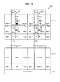
- a multi-block PRAM device 300 is illustrated as including a plurality of PRAM memory blocks 310a to 310n that are electrically coupled to a column decoder/driver circuit 320.
- Each of these PRAM memory blocks 310a to 310n is illustrated as including a plurality of memory cell blocks CBLK1, CBLK2, ... and CBLKm, CBLK(m+1), ....
- Each of these memory cell blocks is electrically coupled to a corresponding pair of word line driver circuits WD, a pair of row decoders XDEC and a pair of local bit line selection circuits YD therein.
- the first memory cell block CBLK1 is electrically coupled in a row direction to a left side word line driver circuit WD11 and a right side word line driver circuit WD12.
- the first memory cell block CBLK1 is electrically coupled in a column direction to a bottom bit line selection circuit YD11 and a top bit line selection circuit YD12.
- a pair of row decoders XDEC are also provided. These row decoders XDEC generate word line driver signals in response to an applied row address.
- the first memory cell block CBLK1 includes a two-dimensional array of PRAM cells 10 containing a plurality of rows and columns. These PRAM cells 10 are illustrated as diode-type PRAM cells, however, transistor-controlled PRAM cells (not shown) may also be used. Each column of PRAM cells 10 is coupled to a corresponding local bit line BL and each row of PRAM cells 10 is coupled to a corresponding word line WL.
- the resistance of each local bit line BL may equal RBL (i.e. 1 ⁇ 2 RBL + 1 ⁇ 2 RBL) and the resistance of each local word line WL may equal RWL (i.e. 1 ⁇ 2 RWL + 1 ⁇ 2 RWL).
- each word line is driven by a corresponding pair of word line drivers, which are connected at opposing ends of the respective word line.
- the illustrated word line WL is driven by a left side word line driver WDC11 and a right side word line driver WDC12. These drivers are illustrated as inverters.
- each local bit line is driven by a corresponding pair of bit line selection devices, which are connected at opposing ends of the respective local bit line.
- the illustrated bit line BL is driven by a bottom bit line selection device BDC11 and a top bit line selection device BDC12.
- These bit line selection devices are illustrated as NMOS transistors having gate terminals responsive to equivalent column selection signals Yi generated within bottom and top bit line selection YD11, YD12.
- the drain terminals of the NMOS transistors are connected to a corresponding global bit line GBL, which is controlled by a column decoder/driver circuit 320.
- the column decoder/driver circuit 320 may be of conventional design.
- the second memory cell block CBLK2 includes a two-dimensional array of PRAM cells 10 containing a plurality of rows and columns of PRAM cells 10.
- the second memory cell block CBLK2 is electrically coupled in a row direction to a left side word line driver circuit WD21 and a right side word line driver circuit WD22.
- the second memory cell block CBLK2 is electrically coupled in a column direction to a bottom bit line selection circuit YD21 and a top bit line selection circuit YD22.
- the illustrated word line WL is driven by a left side word line driver WDC21 and a right side word line driver WDC22.
- the illustrated bit line BL is driven by a bottom bit line selection device BDC21 and a top bit line selection device BDC22.
- bit line selection devices are illustrated as NMOS transistors having gate terminals responsive to equivalent column selection signals Yi generated within bottom and top bit line selection circuits YD21, YD22.
- the drain terminals of the NMOS transistors are connected to a corresponding global bit line GBL, which is controlled by a column decoder/driver circuit 320.
- the memory cell blocks CBLKm and CBLK(m+1) within the PRAM memory block 310n are configured in a similar manner to the first and second memory cell blocks CBLK1 and CBLK2.
- the bottom bit line selection circuit YD11 and the top bit line selection circuit YD12 are configured to electrically connect first and second ends of the local bit line BL to a global bit line GBL during an operation to read data from (or write data to) a selected one of the PRAM memory cells 10 in the corresponding column.
- This electrical connection is provided by the bottom bit line selection device BDC11 and the top bit line selection device BDC12 when the corresponding column selection signal Yi is switched low-to-high.
- This dual connection of opposing ends of the local bit line BL to the corresponding global bit line GBL during reading and programming (i.e., writing) operations increases the slew rate of the local bit line signal by reducing the effective resistance of the local bit line BL as seen by the bit line selection devices. This reduction in effective resistance enables the local bit line BL to be longer for a given read/write access time. This ability to support longer local bit lines by using a pair of bit line selection devices on opposing ends of the local bit line enables the use of larger memory cell blocks (e.g., more rows of memory cells).
- the illustrated left side word line driver WDC11 and a right side word line driver WDC12 are configured to drive opposing ends of the corresponding local word line WL at the same voltage level during an operation to read data from (or write data to) a selected one of the PRAM memory cells 10 in the row.
- This dual connection of opposing ends of the local word line WL during reading and programming (i.e., writing) operations increases the slew rate of the local word line signal and enables the local word line WL to be longer for a given read/write access time.
- This ability to support longer local word lines by using a pair of word line drivers on opposing ends of the word line enables the use of larger memory cell blocks (e.g., more columns of memory cells).
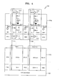
- a multi-block PRAM device 400 is illustrated as including a plurality of PRAM memory blocks 410a - 410n that are electrically coupled to a column decoder/driver circuit 420.
- These PRAM memory blocks 410a - 410n are essentially identical to the PRAM memory blocks 310a - 310n, however, the word line driver circuits WD11, WD12, WD21, WD22, WDm1, WDm2, WD(m+1)1 and WD(m+1)2 illustrated by FIG. 3 are replaced by word line driver circuits WD1, WD2, WD3, WDm, WD(m+1) and WD(m+2).
- These word line driver circuits include drivers (e.g., WDC1, WDC2, WDC3, ...) having outputs connected to intermediate and spaced-apart nodes of a word line that spans multiple memory cell blocks.
- a multi-block PRAM device 500 is illustrated as including a plurality of PRAM memory blocks 510a to 510n that are electrically coupled to a column decoder/driver circuit 520.
- These PRAM memory blocks 510a to 510n are similar to the PRAM memory blocks 310a to 310n, however, the pairs of bit line selection circuits YD11 and YD12, YD21 and YD22, ... are replaced by single-sided bit line selection circuits YD1, YD2, ..., YDm, YD(m+1) ... containing respective bit line selection devices (e.g., BDC1, BDC2, ).
- a multi-block PRAM device 600 is illustrated as including a plurality of PRAM memory blocks 610a to 610n that are electrically coupled to a column decoder/driver circuit 620.
- These PRAM memory blocks 610a to 610n are similar to the PRAM memory blocks 310a to 310n of FIG. 3, however, the pairs of word line driver circuits WD11 and WD12, WD21 and WD22 illustrated by FIG. 3 are replaced by single-sided word line driver circuits WD1, WD2, WDm, WD(m+1), ... having respective word line drivers therein (e.g., WDC1, WDC2, ).
- FIG. 7 illustrates a multi-block PRAM device 700 according to a fifth embodiment of the invention
- the plurality of PRAM memory blocks 410a to 410n illustrated by FIG. 4 are replaced by PRAM memory blocks 710a to 710n, which are electrically coupled to a column decoder/driver circuit 720.
- the PRAM memory blocks 710a to 710n are similar to the PRAM memory blocks 410a to 410n, however, the pairs of bit line selection circuits YD11 and YD12, YD21 and YD22, ... are replaced by single-sided bit line selection circuits YD1, YD2, ... containing respective bit line selection devices (e.g., BDC1, BDC2, ).
Landscapes
- Engineering & Computer Science (AREA)
- Microelectronics & Electronic Packaging (AREA)
- Chemical & Material Sciences (AREA)
- Crystallography & Structural Chemistry (AREA)
- Semiconductor Memories (AREA)
- Static Random-Access Memory (AREA)
Applications Claiming Priority (2)
| Application Number | Priority Date | Filing Date | Title |
|---|---|---|---|
| KR1020050024541A KR100688540B1 (ko) | 2005-03-24 | 2005-03-24 | 메모리 셀의 집적도를 향상시킨 반도체 메모리 장치 |
| US11/348,432 US7397681B2 (en) | 2005-03-24 | 2006-02-06 | Nonvolatile memory devices having enhanced bit line and/or word line driving capability |
Publications (2)
| Publication Number | Publication Date |
|---|---|
| EP1708202A2 true EP1708202A2 (de) | 2006-10-04 |
| EP1708202A3 EP1708202A3 (de) | 2007-02-14 |
Family
ID=36683934
Family Applications (1)
| Application Number | Title | Priority Date | Filing Date |
|---|---|---|---|
| EP06004893A Withdrawn EP1708202A3 (de) | 2005-03-24 | 2006-03-10 | Phasenänderungsspeicher |
Country Status (2)
| Country | Link |
|---|---|
| EP (1) | EP1708202A3 (de) |
| JP (1) | JP2006269062A (de) |
Cited By (3)
| Publication number | Priority date | Publication date | Assignee | Title |
|---|---|---|---|---|
| EP1947652A1 (de) * | 2007-09-13 | 2008-07-23 | STMicroelectronics S.r.l. | Phasenwechsel-Speichervorrichtung mit Fehlerkorrekturfunktion |
| WO2009100108A1 (en) * | 2008-02-05 | 2009-08-13 | Marvell World Trade Ltd. | System and method for decoding a memory array comprising blocks and sub-blocks |
| IT201900025411A1 (it) * | 2019-12-23 | 2021-06-23 | St Microelectronics Srl | Dispositivo di memoria includente un decodificatore di colonna che riduce la caduta di tensione lungo le linee di bit locali selezionate |
Families Citing this family (7)
| Publication number | Priority date | Publication date | Assignee | Title |
|---|---|---|---|---|
| JP2014130676A (ja) * | 2008-03-17 | 2014-07-10 | Ps4 Luxco S A R L | 半導体装置 |
| JP5222619B2 (ja) * | 2008-05-02 | 2013-06-26 | 株式会社日立製作所 | 半導体装置 |
| US8289764B2 (en) | 2008-12-11 | 2012-10-16 | Hitachi, Ltd. | Semiconductor device |
| KR20100104624A (ko) * | 2009-03-18 | 2010-09-29 | 삼성전자주식회사 | 반도체 메모리 소자 |
| US8799560B2 (en) | 2009-08-21 | 2014-08-05 | Hitachi, Ltd. | Semiconductor device |
| JP2013140667A (ja) * | 2013-03-11 | 2013-07-18 | Hitachi Ltd | 半導体装置 |
| US20150071020A1 (en) * | 2013-09-06 | 2015-03-12 | Sony Corporation | Memory device comprising tiles with shared read and write circuits |
Citations (1)
| Publication number | Priority date | Publication date | Assignee | Title |
|---|---|---|---|---|
| US20040125653A1 (en) * | 1999-01-14 | 2004-07-01 | Tran Hieu Van | Seek window verify program system and method for a multilevel non-volatile memory integrated circuit system |
Family Cites Families (5)
| Publication number | Priority date | Publication date | Assignee | Title |
|---|---|---|---|---|
| JPH0632232B2 (ja) * | 1987-07-01 | 1994-04-27 | 日本電気株式会社 | 行デコ−ダ |
| US5526306A (en) * | 1994-02-10 | 1996-06-11 | Mega Chips Corporation | Semiconductor memory device and method of fabricating the same |
| JP3411129B2 (ja) * | 1995-07-03 | 2003-05-26 | 沖電気工業株式会社 | 半導体メモリ |
| US6031784A (en) * | 1998-09-04 | 2000-02-29 | G-Link Technology | Hierarchical decoding of a memory device |
| DE60137788D1 (de) * | 2001-12-27 | 2009-04-09 | St Microelectronics Srl | Architektur einer nichtflüchtigen Phasenwechsel -Speichermatrix |
-
2006
- 2006-03-10 EP EP06004893A patent/EP1708202A3/de not_active Withdrawn
- 2006-03-24 JP JP2006083805A patent/JP2006269062A/ja active Pending
Patent Citations (1)
| Publication number | Priority date | Publication date | Assignee | Title |
|---|---|---|---|---|
| US20040125653A1 (en) * | 1999-01-14 | 2004-07-01 | Tran Hieu Van | Seek window verify program system and method for a multilevel non-volatile memory integrated circuit system |
Cited By (10)
| Publication number | Priority date | Publication date | Assignee | Title |
|---|---|---|---|---|
| EP1947652A1 (de) * | 2007-09-13 | 2008-07-23 | STMicroelectronics S.r.l. | Phasenwechsel-Speichervorrichtung mit Fehlerkorrekturfunktion |
| US7869269B2 (en) | 2007-09-13 | 2011-01-11 | Stmicroelectronics S.R.L. | Phase-change memory device with error correction capability |
| WO2009100108A1 (en) * | 2008-02-05 | 2009-08-13 | Marvell World Trade Ltd. | System and method for decoding a memory array comprising blocks and sub-blocks |
| US8004926B2 (en) | 2008-02-05 | 2011-08-23 | Marvell World Trade Ltd. | System and method for memory array decoding |
| US8203902B2 (en) | 2008-02-05 | 2012-06-19 | Marvell World Trade Ltd. | System and method for memory array decoding |
| US8472277B2 (en) | 2008-02-05 | 2013-06-25 | Marvell World Trade Ltd. | System and method for memory array decoding |
| US8681553B2 (en) | 2008-02-05 | 2014-03-25 | Marvell World Trade Ltd. | System and method for memory array decoding |
| US8891330B2 (en) | 2008-02-05 | 2014-11-18 | Marvell World Trade Ltd. | Method and apparatus for simultaneously accessing a plurality of memory cells in a memory array to perform a read operation and/or a write operation |
| IT201900025411A1 (it) * | 2019-12-23 | 2021-06-23 | St Microelectronics Srl | Dispositivo di memoria includente un decodificatore di colonna che riduce la caduta di tensione lungo le linee di bit locali selezionate |
| US11380393B2 (en) | 2019-12-23 | 2022-07-05 | Stmicroelectronics International N.V. | Memory device and method for coupling a main bitline to two points of a local bitline |
Also Published As
| Publication number | Publication date |
|---|---|
| EP1708202A3 (de) | 2007-02-14 |
| JP2006269062A (ja) | 2006-10-05 |
Similar Documents
| Publication | Publication Date | Title |
|---|---|---|
| US7397681B2 (en) | Nonvolatile memory devices having enhanced bit line and/or word line driving capability | |
| US8040719B2 (en) | Nonvolatile memory devices having bit line discharge control circuits therein that provide equivalent bit line discharge control | |
| JP5396011B2 (ja) | 相変化メモリ装置 | |
| US8238132B2 (en) | Semiconductor device | |
| KR101258983B1 (ko) | 가변저항 소자를 이용한 반도체 메모리 장치 및 그 동작방법 | |
| US8009476B2 (en) | Semiconductor memory device using variable resistor | |
| US7460386B2 (en) | Layout method of a semiconductor memory device | |
| JP5161981B2 (ja) | 半導体装置 | |
| US20080112209A1 (en) | Semiconductor memory device having a three-dimensional cell array structure | |
| TWI497523B (zh) | 非揮發性半導體記憶體裝置 | |
| US7821865B2 (en) | Nonvolatile memory device using variable resistive elements | |
| KR100900135B1 (ko) | 상 변화 메모리 장치 | |
| JP5736988B2 (ja) | 抵抗変化型メモリデバイスおよびその動作方法 | |
| JP2012243359A (ja) | 抵抗変化型メモリデバイスおよびその動作方法 | |
| CN102332294A (zh) | 电阻变化型随机存取存储器装置 | |
| JP2011198445A (ja) | 半導体記憶装置 | |
| CN1885432B (zh) | 相变随机存取存储器器件 | |
| EP1708202A2 (de) | Phasenänderungsspeicher | |
| JP4668668B2 (ja) | 半導体装置 | |
| KR101016958B1 (ko) | 멀티 포트 상변화 메모리 장치 | |
| TW202244928A (zh) | 可變電阻記憶體裝置、包括其的記憶體系統及驅動其的方法 | |
| KR20260064455A (ko) | 프로그래밍가능 저항 메모리 요소를 위한 고장 완화 |
Legal Events
| Date | Code | Title | Description |
|---|---|---|---|
| PUAI | Public reference made under article 153(3) epc to a published international application that has entered the european phase |
Free format text: ORIGINAL CODE: 0009012 |
|
| AK | Designated contracting states |
Kind code of ref document: A2 Designated state(s): AT BE BG CH CY CZ DE DK EE ES FI FR GB GR HU IE IS IT LI LT LU LV MC NL PL PT RO SE SI SK TR |
|
| AX | Request for extension of the european patent |
Extension state: AL BA HR MK YU |
|
| PUAL | Search report despatched |
Free format text: ORIGINAL CODE: 0009013 |
|
| AK | Designated contracting states |
Kind code of ref document: A3 Designated state(s): AT BE BG CH CY CZ DE DK EE ES FI FR GB GR HU IE IS IT LI LT LU LV MC NL PL PT RO SE SI SK TR |
|
| AX | Request for extension of the european patent |
Extension state: AL BA HR MK YU |
|
| 17P | Request for examination filed |
Effective date: 20070809 |
|
| AKX | Designation fees paid |
Designated state(s): DE FR GB |
|
| 17Q | First examination report despatched |
Effective date: 20071004 |
|
| STAA | Information on the status of an ep patent application or granted ep patent |
Free format text: STATUS: THE APPLICATION IS DEEMED TO BE WITHDRAWN |
|
| 18D | Application deemed to be withdrawn |
Effective date: 20080920 |