EP1708351A2 - Systèmes de commande pour onduleurs - Google Patents
Systèmes de commande pour onduleurs Download PDFInfo
- Publication number
- EP1708351A2 EP1708351A2 EP06250548A EP06250548A EP1708351A2 EP 1708351 A2 EP1708351 A2 EP 1708351A2 EP 06250548 A EP06250548 A EP 06250548A EP 06250548 A EP06250548 A EP 06250548A EP 1708351 A2 EP1708351 A2 EP 1708351A2
- Authority
- EP
- European Patent Office
- Prior art keywords
- output
- inverter
- signal
- current
- control system
- Prior art date
- Legal status (The legal status is an assumption and is not a legal conclusion. Google has not performed a legal analysis and makes no representation as to the accuracy of the status listed.)
- Withdrawn
Links
- 238000000034 method Methods 0.000 claims description 10
- 239000003990 capacitor Substances 0.000 description 3
- 238000004146 energy storage Methods 0.000 description 3
- 230000007935 neutral effect Effects 0.000 description 3
- 230000033228 biological regulation Effects 0.000 description 2
- 230000003247 decreasing effect Effects 0.000 description 2
- 238000010586 diagram Methods 0.000 description 2
- 230000000694 effects Effects 0.000 description 1
- 230000005669 field effect Effects 0.000 description 1
- 239000000446 fuel Substances 0.000 description 1
- 238000005259 measurement Methods 0.000 description 1
- 238000010248 power generation Methods 0.000 description 1
Images

Classifications
-
- H—ELECTRICITY
- H02—GENERATION; CONVERSION OR DISTRIBUTION OF ELECTRIC POWER
- H02M—APPARATUS FOR CONVERSION BETWEEN AC AND AC, BETWEEN AC AND DC, OR BETWEEN DC AND DC, AND FOR USE WITH MAINS OR SIMILAR POWER SUPPLY SYSTEMS; CONVERSION OF DC OR AC INPUT POWER INTO SURGE OUTPUT POWER; CONTROL OR REGULATION THEREOF
- H02M7/00—Conversion of AC power input into DC power output; Conversion of DC power input into AC power output
- H02M7/42—Conversion of DC power input into AC power output without possibility of reversal
- H02M7/44—Conversion of DC power input into AC power output without possibility of reversal by static converters
- H02M7/48—Conversion of DC power input into AC power output without possibility of reversal by static converters using discharge tubes with control electrode or semiconductor devices with control electrode
- H02M7/53—Conversion of DC power input into AC power output without possibility of reversal by static converters using discharge tubes with control electrode or semiconductor devices with control electrode using devices of a triode or transistor type requiring continuous application of a control signal
- H02M7/537—Conversion of DC power input into AC power output without possibility of reversal by static converters using discharge tubes with control electrode or semiconductor devices with control electrode using devices of a triode or transistor type requiring continuous application of a control signal using semiconductor devices only, e.g. single switched pulse inverters
- H02M7/5387—Conversion of DC power input into AC power output without possibility of reversal by static converters using discharge tubes with control electrode or semiconductor devices with control electrode using devices of a triode or transistor type requiring continuous application of a control signal using semiconductor devices only, e.g. single switched pulse inverters in a bridge configuration
- H02M7/53871—Conversion of DC power input into AC power output without possibility of reversal by static converters using discharge tubes with control electrode or semiconductor devices with control electrode using devices of a triode or transistor type requiring continuous application of a control signal using semiconductor devices only, e.g. single switched pulse inverters in a bridge configuration with automatic control of output voltage or current
-
- H—ELECTRICITY
- H02—GENERATION; CONVERSION OR DISTRIBUTION OF ELECTRIC POWER
- H02M—APPARATUS FOR CONVERSION BETWEEN AC AND AC, BETWEEN AC AND DC, OR BETWEEN DC AND DC, AND FOR USE WITH MAINS OR SIMILAR POWER SUPPLY SYSTEMS; CONVERSION OF DC OR AC INPUT POWER INTO SURGE OUTPUT POWER; CONTROL OR REGULATION THEREOF
- H02M1/00—Details of apparatus for conversion
- H02M1/0003—Details of control, feedback or regulation circuits
- H02M1/0025—Arrangements for modifying reference values, feedback values or error values in the control loop of a converter
Definitions
- the present invention relates to DC to AC inverters, and in particular to control systems for DC to AC inverters.
- DC to AC invertors are used for converting a source of DC power into AC power.
- the DC power source may produce DC power directly, for example from one or more batteries, or it may be an intermediate DC source produced by rectifying an AC supply for example from an AC generator.
- CMOS complementary metal-oxide-semiconductor
- PWM pulse width modulator
- a reference signal generator is used in order to generate a reference signal which has a waveform which is substantially the same as the waveform which it is desired to create at the inverter output.
- a detector detects an actual output signal at the inverter output, and this is compared to the reference signal in order to produce an error signal.
- a controller receives the error signal and adjusts the output of the PWM such that the instantaneous output of the inverter matches as far as possible the instantaneous value of the reference signal. In this way the output of the inverter can be made to track the reference signal, so that the output waveform is substantially the same as the reference waveform. Under ideal conditions this results in a constant RMS voltage or current at the output.
- a problem which has been found in known inverters is that the RMS output may vary in dependence on the load.
- the RMS output voltage may either decrease or increase in dependence on the size and type of the load.
- the control system should correct the change in output, in practice it has been found that inaccuracies in the control system may result in the change in output not being fully compensated, particularly with large and/or reactive loads. Previous attempts to solve this problem have involved increasing the gain of the control system so as to reduce any inaccuracies. However, increasing the gain of the control system may lead to instability.
- control system for a DC to AC inverter, the control system comprising:
- the present invention recognises that a change in the output of the inverter (due for example to a change in the size or type of load) can be compensated for by adjusting the amplitude of the reference signal itself.
- a change in the output voltage can be reduced or corrected.
- the present invention may also allow the gain of the control system to be less than would otherwise be the case, which may reduce the likelihood of instability in the system.
- control means attempts to ensure that the waveform at the inverter output is the same as that of the reference signal, in practice there will be some deviation due to the latency of the control system and any error therein.
- the measure of the inverter output is preferably an average value of the inverter output.
- the measure of the inverter output may be an RMS value, or some other average value. This can allow a change in the average output of the inverter (due for example to a change in the load) to be reduced or corrected.
- the measure of the inverter output may be some other measure, such as peak value, peak to peak value, mean to peak value or an instantaneous value at a predetermined point in the cycle of the output waveform.
- the measure which is chosen will depend upon which characteristics of the output signal it is desired to correct. Such a value may be measured every cycle or once every few cycles, and the measured value used to adjust the amplitude of the reference signal. An average of a number of instantaneous values may also be used.
- the characteristic of the reference signal which is adjusted is the same as the characteristic of the output signal which the measure represents.
- the measure represents the RMS value at the inverter output
- the RMS value of the reference signal is preferably adjusted by the adjusting means.
- the adjusting means may comprise means for generating a second reference signal, and means for comparing the second reference signal with the measure of the inverter output to produce an error signal representing an error in the measure of the inverter output.
- the adjusting means may further comprise a reference signal control unit for receiving the error signal and producing an adjustment signal for adjusting the reference signal produced by the generating means.
- the reference signal control unit may comprise at least one of: a proportional regulator; a proportional integral regulator; a proportional differential regulator; or a proportional integral differential regulator.
- the reference signal control unit may comprise a limiter for limiting the amount by which the amplitude of the reference signal can be adjusted. This may ensure that large changes in the amplitude of the reference signal do not take place, which may therefore ensure that large changes in the inverter output do not take place. This can help to protect the control system and ensure its stability.
- the limiter may limit changes to 5% in any one cycle, or some other amount.
- the limiter may set a limit to the absolute amount by which the amplitude of the reference signal can be adjusted, or it may set a limit to the rate at which it can be adjusted, or both. Either or both limits may be fixed or variable.
- the reference signal generator may comprise means for generating an alternating waveform (such as a sine wave), an amplitude generator for generating an amplitude value representing the amplitude of the reference signal, and combining means (such as a multiplier) for combining the alternating waveform with the amplitude value.
- the adjusting means may be arranged to adjust the amplitude value output by the amplitude generator. For example, the output of the adjusting means may be added to or subtracted from the output of the amplitude generator, or the adjusting means may adjust a control signal supplied to the amplitude generator. Alternatively the adjusting means may be arranged to multiply the reference signal by an appropriate factor.
- the control system may further comprise a sensor for sensing a signal at the output of the inverter, and a comparator for comparing the output signal with the reference signal to produce an error signal, and the control means may be arranged to control the inverter in dependence on the value of the error signal.
- the sensor, comparator and control means form a feedback loop, and the latency of the feedback loop is smaller than the period of the AC output signal.
- the latency of the feedback loop may be less than 25% of the period of the output signal, or less than 10%, 5% or 1%. In this way the instantaneous output of the inverter can be made to track the instantaneous value of the reference signal as closely as possible.
- control system is arranged to control the inverter output voltage, so as to produce an output having a desired voltage waveform.
- the generating means may therefore be arranged to generate a reference voltage signal, and the measure of the inverter output may be a measure of the voltage at the inverter output.
- the measure of the voltage may be an average value of the voltage, such as the RMS value.
- control system may comprise an outer voltage feedback loop and an inner current feedback loop.
- the current feedback loop may comprise a current sensor, means for comparing the sensed current with a reference current signal, and a current control unit.
- the reference current signal may be produced by the outer voltage feedback loop.
- the outer voltage feedback loop may comprise a voltage sensor, a comparator for comparing the sensed voltage with the reference signal, and a control unit for producing the reference current signal.
- the determining means may be arranged to determine the measure of the voltage at the inverter output based on the sensed voltage. For example, if the measure is a measure of the RMS voltage, then the determining means may comprise means for receiving the sensed voltage, and means for determining the RMS voltage therefrom. This can avoid the need to provide a separate voltage sensor.
- control system is arranged to control the inverter output current, so as to produce an output having a desired current waveform.
- the generating means may therefore be arranged to generate a reference current signal, and the measure of the inverter output may be a measure of the current at the inverter output.
- the measure of the current may be an average value of the current, such as the RMS value.
- control system may further comprise a current sensor for sensing the current at the output of the inverter, and a comparator for comparing the sensed current with the reference current signal to produce an error signal for controlling the inverter.
- the determining means may be arranged to receive an output of the current sensor and to determine the measure of the current at the inverter output in dependence thereon.
- control means may comprise one or more of: a proportional regulator; a proportional integral regulator; a proportional differential regulator; a proportional integral differential regulator; or any other type of regulator.
- the control means may be arranged to control the output voltage or the output current, or both.
- control means may comprise a pulse width modulator (PWM) for producing pulses with modulated pulse width.
- PWM pulse width modulator
- the PWM preferably produces an output signal comprising pulses whose width is modulated by the signal it is desired to create at the output of the inverter.
- the frequency of the output pulses is preferably higher than the frequency of the AC output signal.
- the frequency of the output pulses may be twice the frequency of the AC output signal, or more, such as more than 10, 20, 50 or 100 times the frequency.
- the present invention also provides an inverter comprising a control system in any of the forms described above.
- the inverter may comprise a pair of switches arranged to switch a positive and negative DC voltage alternately to an output terminal. Where the AC output signal has more than one phase (for example, three phases) a pair of switches may be provided for each phase.
- the switches may be transistors such as insulated gate bipolar transistors (IGBT), or field effect transistors (FET) or any other type of transistors.
- the inverter also comprises a filter arranged to attenuate frequency components of the output signal at the frequency of the pulses, relative to the fundamental AC output frequency.
- the inverter may be used in any situation where it is desired to convert a DC voltage to an AC voltage.
- the inverter may be used in a generating set comprising an AC generator and an AC to DC converter (such as a rectifier) for producing the DC voltage.
- the present invention also provides a generating set comprising an AC generator, an AC to DC converter, a DC to AC inverter, and a control system in any of the forms described above.
- the generating set may be as described in WO 01/56133 in the name of Newage International Limited, the entire contents of which are incorporated herein by reference.
- the present invention also provides a corresponding method, and thus according to another aspect of the invention there is provided a method of controlling a DC to AC inverter, the method comprising the steps of:
- control system for a DC to AC inverter, the control system comprising:
- the present invention may be implemented in hardware, or as software modules running on a processor, or in any combination of the two.
- WO98/28832 in the name of Newage International Limited, the contents of which hare incorporated herein by reference, discloses a generating set which comprises an engine/generator which provides a variable voltage electrical output, this output being rectified and fed to a DC to DC converter, the output DC voltage of the DC to DC converter being monitored by a control circuit and serving as an intermediate DC output which is fed to a DC to AC inverter to generate an AC output which supplies an external load.
- the DC to DC converter decouples or isolates the intermediate DC output from the fluctuations in the current and/or voltage output of the generator so that the apparatus is able to accommodate substantial variations in the output of the generator while maintaining the intermediate DC output within desired operating parameters.
- the DC to DC converter also serves to decouple or isolate the generator from variations in the load.
- An energy storage device for example a capacitor, is connected in parallel with the DC link and thereby provides a short term energy reserve when the load applied to the DC link voltage varies suddenly.
- This energy storage device may be supplemented by other similar devices with respective control systems. In some cases such supplementary energy storage devices may be excluded. Instead a load anticipation circuit may be introduced to cope with high impact or step loads.
- control circuit includes various electronic controllers which monitor and control the output voltage and current of the inverter and the intermediate DC output or link voltage.
- the measurement and control circuit of the generating set disclosed in WO98/28832 monitors the generator output voltage and current together with the DC link voltage and operates through a feedback control loop to vary the speed of the engine so as maintain the DC link voltage constant and limit the generator output current to a level determined a current reference signal.
- FIG 1 shows an overview of a DC/AC inverter to which the present invention may be applied.
- a three phase DC/AC inverter has a power output terminal U,V,W for each phase and a neutral terminal N.
- the inverter is connected to a DC voltage shown as Ua and Ub in Figure 1.
- the inverter includes a pair of capacitors Ca1 and Cb1 which are connected in series across the DC voltage.
- the AC power output for each phase of the three phase output of the inverter is produced by operation of a respective one of three pairs of transistors Tau and Tbu; Tav and Tbv; and Taw and Tbw which are connected in parallel with one another.
- the transistors of each pair are series connected by having the emitter of one of that pair connected to the collector of the other of that pair, the series connection between the transistors of each pair being connected to the respective power output terminal U,V,W through a respective inductor Lu, Lv, Lw.
- Each of the inductors Lu, Lv and Lw is the inductor of an LC filter which is provided for each phase.
- the capacitor Cu, Cv, Cw of each LC filter is connected between the output line for the respective phase and the neutral.
- each of the transistors Taw, Tbw, Tav, Tbv, Tau and Tbu is an insulated Gate Bipolar Transistor (IGBT) and has an inverse parallel diode connected across its emitter and collector junctions (diode cathode to collector, diode anode to emitter).
- IGBT insulated Gate Bipolar Transistor
- Other forms of transistor such as FETS could be used.
- a voltage sensor VSuvw senses the output voltage of each of the AC power outputs for each phase U, V and W with respect to the neutral line N.
- the voltage sensor VSuvw has three outputs which are fed to respective inputs of an Inverter controller IC, which also receives the three output signals from current sensors CSu, CSv and CSw at respective ones of three further inputs.
- the Inverter controller IC also receives three reference signals, representing the required value of output frequency and voltage, which are provided by a reference signal generator.
- the inverter controller IC uses the inductor (choke) currents measured by the current sensors CSu, CSv and CSw to produce a feedback signal for current regulation.
- the inverter controller IC has six outputs Taw, Tbw, Tav, Tbv, Tau and Tbu, which are each connected to the base of a respective one of the output transistors Taw, Tbw, Tav, Tbv, Tau and Tbu.
- the inverter controller IC thereby operates to control operation of the transistors Taw, Tbw, Tav, Tbv, Tau and Tbu of the inverter by pulse width modulation.
- the DC/AC pulse width modulated inverter produces a sinusoidal three phase voltage for symmetrical and non-symmetrical loads.
- the output voltage of each phase U,V,W is individually modulated by the Inverter Controller IC.
- Figure 1 shows a three phase inverter
- the present invention can be applied to a single phase inverter, or an inverter having any other number of phases.
- Figure 1 shows an inverter with current control and voltage control, either current control alone or voltage control alone could be used.
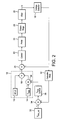
- FIG. 2 is a block diagram of parts of a DC/AC inverter in accordance with one embodiment. For simplicity, only a single phase is shown.
- the inverter comprises a reference voltage signal generator 10 which generates a reference voltage signal which has a waveform which is substantially the same as the waveform which it is desired to create at the inverter output.
- the desired output waveform is a sine wave having a frequency ⁇ and a peak voltage U max
- the reference signal generator therefore comprises a sine wave generator 12 which generates a sine wave of frequency ⁇ , and an amplitude generator 14 which generates an amplitude value of U max .
- the sine wave and amplitude value are combined in multiplier 16 to produce the reference signal.
- a voltage sensor 18 measures an instantaneous voltage at the output of the inverter.
- the instantaneous value of the output voltage is compared to the instantaneous value of the reference voltage in comparator 20.
- the output of comparator 20 is thus an error signal representing a difference between the actual instantaneous output of the inverter and a desired output of the inverter.
- Control unit 22 processes the error signal in order to produce a control signal.
- Control unit 22 may be, for example, a proportional (P) regulator, a proportional integral (PI) regulator, a PD (proportional and derivative) regulator or a proportional integral derivative (PID) regulator, or any other type of regulator, as appropriate. Regulators of these types are known in the art and thus are not described further.
- the control signal output from control unit 22 is fed to PWM 24.
- PWM 24 produces a relatively high frequency pulsed signal which is pulse width modulated with the waveform that it is desired to produce at the inverter output.
- the pulse width modulated signal is used to drive switches in the output stage 26 in order to produce an AC voltage.
- the AC voltage is filtered in filter 28 in order to remove the high frequency component present in the pulse width modulated signal, and thereby to produce the AC output signal.
- control unit 22 is to ensure that the instantaneous voltage at the output of the inverter tracks the instantaneous voltage of the reference signal as closely as possible. In this way the shape of the inverter output voltage is made substantially the same as the shape of the reference signal.
- the inverter also comprises RMS (root mean square) reference voltage generator 30, RMS calculation unit 32, adder 34, RMS control unit 36, and adder 38.
- RMS reference voltage generator 30 produces an RMS reference voltage which is the desired RMS voltage at the inverter output.
- RMS calculation unit 32 calculates an RMS value of the actual inverter output voltage. The calculated value of the RMS voltage is compared to the reference voltage in comparator 34. The output of comparator 34 is thus an error signal which indicates how far the actual RMS output voltage deviates from the reference RMS voltage.
- the error signal output from comparator 34 is fed to RMS control unit 36, which processes the error signal in order to produce an RMS correction signal.
- the RMS correction signal output from the control unit 36 is fed to adder 38, where it is added to the output of amplitude generator 14.
- the output of the RMS control unit 36 modifies the output of amplitude generator 14 in dependence on the difference between the desired RMS voltage and the actual RMS voltage at the inverter output. In this way the peak value of the reference voltage itself is adjusted in dependence on the difference between the desired RMS voltage and the actual RMS voltage.
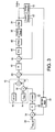
- FIG 3 shows parts of an inverter in another embodiment.
- an inner current control loop is provided to control the inductor (choke) current directly.
- parts of the inverter which are in common with the inverter shown in Figure 2 are given the same reference numeral and are not described further.
- PI regulator 40 receives a voltage error signal from adder 20, which error signal represents the difference between the instantaneous actual output voltage and the instantaneous reference voltage. PI regulator 40 acts on the voltage error signal to produce an output signal which is, in effect, a signal indicating the amount of current that is needed in the inductor of the inverter to achieve the desired output voltage.
- a current sensor 42 senses the current in the inductor of the inverter. The sensed current is compared to the output of PI regulator 40 in comparator 44. The output of comparator 44 is thus a current error signal indicating an error in the current in the inductor. The output of comparator 44 is fed to PID regulator 46. PID regulator 46 acts on the current error signal using proportional terms, integral terms, and differential terms to produce an output signal which is a control signal for PWM 48.
- PWM 48 produces a pulsed signal at a relatively high frequency which is pulse width modulated with the signal which it is desired to produce at the inverter output.
- the pulse frequency may be 15kHz, and it may be modulated with a 50 or 60 Hz sine wave having a 311 V peak voltage (220V RMS).
- the pulse width modulated signal is supplied to the switches in the output stage 26 in order to switch the DC signal to produce an AC output signal in the manner described above with reference to Figure 1.
- the inverter shown in Figure 3 also includes PI regulator 50 and limiter 52, which are part of the feedback loop which controls the peak value of the reference voltage.
- PI regulator 50 acts on the RMS error signal output from comparator 34 using proportional terms and integral terms to produce the RMS correction signal.
- Limiter 52 ensures that the value of the RMS correction signal does not exceed certain limits, which may be fixed or variable.
- the output of limiter 52 is fed to adder 38, in order to add the RMS correction signal to the peak reference voltage in the way described above with reference to Figure 2.
- any of PI regulator 40, PID regulator 46 and PI regulator 50 may be replaced with a P regulator, a PI regulator, a PD regulator or a PID regulator, or indeed with any other type of regulator, as appropriate.
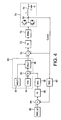
- FIG. 4 shows parts of an inverter in a further embodiment.
- the inverter shown in Figure 4 makes use of an RMS current controller in order to regulate the RMS current at the output of the inverter. Regulation of the RMS current may be required, for example, when a generating apparatus is in a grid connection mode where current is being injected into a grid.
- the inverter comprises a reference current signal generator 60 which generates a reference current signal which has a waveform which is substantially the same as the waveform which it is desired to create at the inverter output.
- the desired output waveform is a sine wave having a frequency ⁇ and a peak voltage U max
- the reference signal generator therefore comprises a sine wave generator 62 which generates a sine wave of frequency ⁇ , and an amplitude generator 64 which generates an amplitude value of U max .
- the sine wave and amplitude value are combined in multiplier 66 to produce the reference signal.
- a current sensor 68 measures an instantaneous current at the output of the inverter.
- the instantaneous value of the output current is compared to the instantaneous value of the reference current in comparator 70.
- the output of comparator 70 is thus an error signal representing a difference between the actual instantaneous current output of the inverter and a desired current output of the inverter.
- control unit 72 which processes the error signal in order to produce a control signal.
- control unit 72 is a proportional integral (PI) regulator, although it may be, for example, a proportional (P) regulator, a PD (proportional and derivative) regulator or a proportional integral derivative (PID) regulator, or any other type of regulator, as appropriate.
- PI proportional integral
- control signal output from control unit 72 is fed to PWM 74.
- PWM 74 produces a relatively high frequency pulsed signal which is pulse width modulated with the waveform that it is desired to produce at the inverter output.
- the pulse width modulated signal is used to drive switches in the output stage 76 in order to produce an AC output.
- the AC output is filtered by LC filter 78 in order to remove the high frequency component present in the pulse width modulated signal, and thereby to produce the AC output signal.
- the task of the control unit 72 is to ensure that the instantaneous current at the output of the inverter tracks the instantaneous value of the reference signal as closely as possible. In this way the shape of the inverter output current is made substantially the same as the shape of the reference signal.
- the inverter also comprises RMS (root mean square) current reference generator 80, RMS calculation unit 82, adder 84, RMS control unit 86, limiter 88 and adder 90.
- RMS current reference generator 80 produces an RMS reference signal which represents the desired RMS current at the inverter output.
- RMS calculation unit 82 calculates an RMS value of the actual inverter output current. The calculated value of the RMS current is compared to the current reference signal in comparator 84. The output of comparator 84 is thus an error signal which indicates how far the actual RMS output current deviates from the reference RMS current.
- the error signal output from comparator 84 is fed to RMS control unit 86, which processes the error signal in order to produce an RMS correction signal.
- the RMS correction signal output from the control unit 86 is fed to limiter 88.
- Limiter 88 ensures that the value of the RMS correction signal does not exceed certain limits, which may be fixed or variable.
- the output of limiter 88 is fed to adder 90, where it is added to the output of amplitude generator 64.
- the output of the RMS control unit 86 modifies the output of amplitude generator 64 in dependence on the difference between the desired RMS current and the actual RMS current at the inverter output.
- any of the inverters described above can be used as part of a generating system such as that described in WO 01/56133 or WO98/28832 referred to above.
Landscapes
- Engineering & Computer Science (AREA)
- Power Engineering (AREA)
- Inverter Devices (AREA)
Applications Claiming Priority (1)
| Application Number | Priority Date | Filing Date | Title |
|---|---|---|---|
| GBGB0502045.8A GB0502045D0 (en) | 2005-02-01 | 2005-02-01 | Control system for DC to AC inverters |
Publications (2)
| Publication Number | Publication Date |
|---|---|
| EP1708351A2 true EP1708351A2 (fr) | 2006-10-04 |
| EP1708351A3 EP1708351A3 (fr) | 2006-10-11 |
Family
ID=34307786
Family Applications (1)
| Application Number | Title | Priority Date | Filing Date |
|---|---|---|---|
| EP06250548A Withdrawn EP1708351A3 (fr) | 2005-02-01 | 2006-02-01 | Systèmes de commande pour onduleurs |
Country Status (2)
| Country | Link |
|---|---|
| EP (1) | EP1708351A3 (fr) |
| GB (1) | GB0502045D0 (fr) |
Cited By (4)
| Publication number | Priority date | Publication date | Assignee | Title |
|---|---|---|---|---|
| WO2013148410A3 (fr) * | 2012-03-28 | 2013-12-19 | Mks Instruments, Inc. | Alimentation électrique compacte configurable pour exciter des cellules de production d'ozone |
| TWI513171B (zh) * | 2011-10-13 | 2015-12-11 | Delta Electronics Inc | 高效率控制之整合式逆變器裝置及其操作方法 |
| WO2020068090A1 (fr) * | 2018-09-28 | 2020-04-02 | Innovative Power Solutions, Llc | Commande de processus utilisant une boucle de commande d'amplitude |
| CN113411004A (zh) * | 2021-07-14 | 2021-09-17 | 深圳市洛仑兹技术有限公司 | 一种逆变电桥控制电路和电控设备 |
Families Citing this family (1)
| Publication number | Priority date | Publication date | Assignee | Title |
|---|---|---|---|---|
| US9997977B1 (en) | 2016-02-22 | 2018-06-12 | MWE Investments LLC | Dual engine generator |
Citations (2)
| Publication number | Priority date | Publication date | Assignee | Title |
|---|---|---|---|---|
| WO1998028832A1 (fr) | 1996-12-20 | 1998-07-02 | Manuel Dos Santos Da Ponte | Dispositif generateur hybride |
| WO2001056133A1 (fr) | 2000-01-28 | 2001-08-02 | Newage International Limited | Systeme generateur de courant alternatif |
Family Cites Families (7)
| Publication number | Priority date | Publication date | Assignee | Title |
|---|---|---|---|---|
| US4468724A (en) * | 1981-04-08 | 1984-08-28 | Hitachi, Ltd. | Method and apparatus for controlling load current |
| JPH03164093A (ja) * | 1989-11-17 | 1991-07-16 | Matsushita Electric Ind Co Ltd | 電流検出方法 |
| WO1992015148A1 (fr) * | 1991-02-22 | 1992-09-03 | U.S. Windpower, Inc. | Unite de commande de moteur a quatre cadrans |
| JP3022063B2 (ja) * | 1993-01-07 | 2000-03-15 | 三菱電機株式会社 | 電力変換器の制御装置 |
| EP2267859A3 (fr) * | 2001-07-23 | 2014-08-13 | Northern Power Systems Utility Scale, Inc. | Système de commande pour convertisseur de puissance et procédé de contrôle du fonctionnement d'un convertisseur de puissance |
| US6791850B2 (en) * | 2001-10-23 | 2004-09-14 | Delta Electronics, Inc. | DC-to-AC power inverter and method of operation thereof |
| US6850425B2 (en) * | 2003-01-10 | 2005-02-01 | Delta Electronics, Inc. | Parallel inverter system based on tracking of system power reference |
-
2005
- 2005-02-01 GB GBGB0502045.8A patent/GB0502045D0/en not_active Ceased
-
2006
- 2006-02-01 EP EP06250548A patent/EP1708351A3/fr not_active Withdrawn
Patent Citations (2)
| Publication number | Priority date | Publication date | Assignee | Title |
|---|---|---|---|---|
| WO1998028832A1 (fr) | 1996-12-20 | 1998-07-02 | Manuel Dos Santos Da Ponte | Dispositif generateur hybride |
| WO2001056133A1 (fr) | 2000-01-28 | 2001-08-02 | Newage International Limited | Systeme generateur de courant alternatif |
Cited By (10)
| Publication number | Priority date | Publication date | Assignee | Title |
|---|---|---|---|---|
| TWI513171B (zh) * | 2011-10-13 | 2015-12-11 | Delta Electronics Inc | 高效率控制之整合式逆變器裝置及其操作方法 |
| WO2013148410A3 (fr) * | 2012-03-28 | 2013-12-19 | Mks Instruments, Inc. | Alimentation électrique compacte configurable pour exciter des cellules de production d'ozone |
| CN104321273A (zh) * | 2012-03-28 | 2015-01-28 | Mks仪器股份有限公司 | 用于为臭氧生产单元提供能量的紧凑的、可配置电源 |
| US9302912B2 (en) | 2012-03-28 | 2016-04-05 | Mks Instruments, Inc. | Compact, configurable power supply for energizing ozone-producing cells |
| CN104321273B (zh) * | 2012-03-28 | 2016-09-07 | Mks仪器股份有限公司 | 用于为臭氧生产单元提供能量的紧凑的、可配置电源 |
| US9865426B2 (en) | 2012-03-28 | 2018-01-09 | Mks Instruments, Inc. | Compact, configurable power supply for energizing ozone-producing cells |
| EP3713072A1 (fr) * | 2012-03-28 | 2020-09-23 | MKS Instruments, Inc. | Alimentation électrique compacte configurable pour exciter des cellules de production d'ozone |
| WO2020068090A1 (fr) * | 2018-09-28 | 2020-04-02 | Innovative Power Solutions, Llc | Commande de processus utilisant une boucle de commande d'amplitude |
| US11394286B2 (en) | 2018-09-28 | 2022-07-19 | Safran Power Usa, Llc | Process control using amplitude control loop |
| CN113411004A (zh) * | 2021-07-14 | 2021-09-17 | 深圳市洛仑兹技术有限公司 | 一种逆变电桥控制电路和电控设备 |
Also Published As
| Publication number | Publication date |
|---|---|
| EP1708351A3 (fr) | 2006-10-11 |
| GB0502045D0 (en) | 2005-03-09 |
Similar Documents
| Publication | Publication Date | Title |
|---|---|---|
| US6771522B2 (en) | Inverter parallel operation system | |
| US7660135B2 (en) | Universal AC high power inveter with galvanic isolation for linear and non-linear loads | |
| AU2008227057B2 (en) | Motor drive using flux adjustment to control power factor | |
| JP5054083B2 (ja) | 風力タービン及びその運転方法 | |
| US7420351B2 (en) | Power-factor correction device for variable speed drive | |
| US8503205B2 (en) | AC/DC converter with a PFC and a DC/DC converter | |
| US9634602B2 (en) | Three-phase inverter apparatus and control method thereof | |
| JPWO2010086929A1 (ja) | 電力変換装置 | |
| KR19990077114A (ko) | 다중레벨 전력변환장치 | |
| KR101562848B1 (ko) | 능동댐핑기반 반복제어기법을 이용한 무정전전원장치 제어 방법 | |
| US7869232B2 (en) | Electric power converter suppressing output voltage variation due to input voltage fluctuation | |
| JP3873972B2 (ja) | 電源装置およびこの電源装置を構成するコンバータ部のスイッチング素子をオン/オフ制御するスイッチング信号の作成方法 | |
| KR101484064B1 (ko) | 신재생 에너지의 전력제어장치 | |
| EP1708351A2 (fr) | Systèmes de commande pour onduleurs | |
| JP2013048504A (ja) | 太陽光発電設備 | |
| US20120113691A1 (en) | Power converter with controlled current source | |
| JP6837576B2 (ja) | 電力変換装置 | |
| JP2001268924A (ja) | 携帯用発電機の出力電圧修正方法 | |
| GB2450891A (en) | Cycloconverter | |
| JP3541887B2 (ja) | 電力変換装置 | |
| JP2008228439A (ja) | 電力変換装置及びその安定化方法 | |
| Ali et al. | Experimental validation of a Low-Voltage Back-to-Back Converter Control Strategy | |
| US20080157598A1 (en) | Power converting apparatus | |
| JP5528730B2 (ja) | 電力変換装置 | |
| US20260121418A1 (en) | Method of adaptively controlling charging module according to load variation |
Legal Events
| Date | Code | Title | Description |
|---|---|---|---|
| PUAI | Public reference made under article 153(3) epc to a published international application that has entered the european phase |
Free format text: ORIGINAL CODE: 0009012 |
|
| PUAL | Search report despatched |
Free format text: ORIGINAL CODE: 0009013 |
|
| AK | Designated contracting states |
Kind code of ref document: A2 Designated state(s): AT BE BG CH CY CZ DE DK EE ES FI FR GB GR HU IE IS IT LI LT LU LV MC NL PL PT RO SE SI SK TR |
|
| AX | Request for extension of the european patent |
Extension state: AL BA HR MK YU |
|
| AK | Designated contracting states |
Kind code of ref document: A3 Designated state(s): AT BE BG CH CY CZ DE DK EE ES FI FR GB GR HU IE IS IT LI LT LU LV MC NL PL PT RO SE SI SK TR |
|
| AX | Request for extension of the european patent |
Extension state: AL BA HR MK YU |
|
| RAP1 | Party data changed (applicant data changed or rights of an application transferred) |
Owner name: CUMMINS GENERATOR TECHNOLOGIES LIMITED |
|
| 17P | Request for examination filed |
Effective date: 20070402 |
|
| AKX | Designation fees paid |
Designated state(s): AT BE BG CH CY CZ DE DK EE ES FI FR GB GR HU IE IS IT LI LT LU LV MC NL PL PT RO SE SI SK TR |
|
| 17Q | First examination report despatched |
Effective date: 20070529 |
|
| STAA | Information on the status of an ep patent application or granted ep patent |
Free format text: STATUS: THE APPLICATION IS DEEMED TO BE WITHDRAWN |
|
| 18D | Application deemed to be withdrawn |
Effective date: 20071009 |