EP1708476A2 - Optisches Bauelement-Modul - Google Patents
Optisches Bauelement-Modul Download PDFInfo
- Publication number
- EP1708476A2 EP1708476A2 EP06251791A EP06251791A EP1708476A2 EP 1708476 A2 EP1708476 A2 EP 1708476A2 EP 06251791 A EP06251791 A EP 06251791A EP 06251791 A EP06251791 A EP 06251791A EP 1708476 A2 EP1708476 A2 EP 1708476A2
- Authority
- EP
- European Patent Office
- Prior art keywords
- transparent lid
- image sensor
- sensing unit
- solid
- optical path
- Prior art date
- Legal status (The legal status is an assumption and is not a legal conclusion. Google has not performed a legal analysis and makes no representation as to the accuracy of the status listed.)
- Withdrawn
Links
Images



Classifications
-
- H—ELECTRICITY
- H04—ELECTRIC COMMUNICATION TECHNIQUE
- H04N—PICTORIAL COMMUNICATION, e.g. TELEVISION
- H04N1/00—Scanning, transmission or reproduction of documents or the like, e.g. facsimile transmission; Details thereof
- H04N1/024—Details of scanning heads ; Means for illuminating the original
-
- H—ELECTRICITY
- H04—ELECTRIC COMMUNICATION TECHNIQUE
- H04N—PICTORIAL COMMUNICATION, e.g. TELEVISION
- H04N23/00—Cameras or camera modules comprising electronic image sensors; Control thereof
- H04N23/57—Mechanical or electrical details of cameras or camera modules specially adapted for being embedded in other devices
-
- H—ELECTRICITY
- H10—SEMICONDUCTOR DEVICES; ELECTRIC SOLID-STATE DEVICES NOT OTHERWISE PROVIDED FOR
- H10W—GENERIC PACKAGES, INTERCONNECTIONS, CONNECTORS OR OTHER CONSTRUCTIONAL DETAILS OF DEVICES COVERED BY CLASS H10
- H10W72/00—Interconnections or connectors in packages
- H10W72/851—Dispositions of multiple connectors or interconnections
- H10W72/874—On different surfaces
- H10W72/884—Die-attach connectors and bond wires
-
- H—ELECTRICITY
- H10—SEMICONDUCTOR DEVICES; ELECTRIC SOLID-STATE DEVICES NOT OTHERWISE PROVIDED FOR
- H10W—GENERIC PACKAGES, INTERCONNECTIONS, CONNECTORS OR OTHER CONSTRUCTIONAL DETAILS OF DEVICES COVERED BY CLASS H10
- H10W90/00—Package configurations
- H10W90/701—Package configurations characterised by the relative positions of pads or connectors relative to package parts
- H10W90/731—Package configurations characterised by the relative positions of pads or connectors relative to package parts of die-attach connectors
- H10W90/732—Package configurations characterised by the relative positions of pads or connectors relative to package parts of die-attach connectors between stacked chips
-
- H—ELECTRICITY
- H10—SEMICONDUCTOR DEVICES; ELECTRIC SOLID-STATE DEVICES NOT OTHERWISE PROVIDED FOR
- H10W—GENERIC PACKAGES, INTERCONNECTIONS, CONNECTORS OR OTHER CONSTRUCTIONAL DETAILS OF DEVICES COVERED BY CLASS H10
- H10W90/00—Package configurations
- H10W90/701—Package configurations characterised by the relative positions of pads or connectors relative to package parts
- H10W90/751—Package configurations characterised by the relative positions of pads or connectors relative to package parts of bond wires
- H10W90/754—Package configurations characterised by the relative positions of pads or connectors relative to package parts of bond wires between a chip and a stacked insulating package substrate, interposer or RDL
Definitions
- the present invention relates to an optical device module incorporated in digital cameras, camera phones and the like and having a solid-state image sensor for photographing a subject, and a method of fabricating the optical device module.
- a solid-state image sensor provided in digital cameras, camera phones and the like is for capturing the subject to be photographed.
- the solid-state image sensor is integrated into a module together with a lens, an infrared intercepting material and a signal processor processing the image information captured by the image sensor, and is provided as an optical device module.
- digital cameras, camera phones and the like incorporating the optical device module have been reduced in size, and the optical device module has also been reduced in size.
- the optical center of the pixel area of the solid-state image sensor coincide with the optical center of the lens, and it is also necessary that the plane formed by the pixel area be orthogonal to the optical axis of the lens.
- the accuracy of the positioning of the lens with respect to the solid-state image sensor is low, a problem occurs such that focus cannot be achieved or that the image captured by the solid-state image sensor is dark.
- an adjustment mechanism for adjusting focus is provided, and focus adjustment is performed after the optical device module is fabricated.
- the provision of the adjustment mechanism hinders the size reduction of the optical device module.
- Japanese Patent Application Laid-Open No. 2003-110946 proposes an image sensor module package in which a solid-state image sensor is bonded onto a circuit board, a housing holding an IR filter is bonded onto the circuit board so as to cover the solid-state image sensor, and a holder holding a lens is fixed to the housing.
- the fabrication process is simplified by fixing the holder and the housing by press fitting.
- Japanese Patent Application Laid-Open No. 2004-297282 proposes a camera module in which a holder holding a lens and an optical filter is fixed by a bonding agent onto a package where an image sensor is fixed.
- the holder is bonded by use of two kinds of bonding agents, a volatile curing bonding agent that cures by the volatilization of the solvent and an ultraviolet curing bonding agent that cures by the application of ultraviolet light, the lens position is adjusted after temporary bonding, and after the position is determined, the bonding agent is cured to thereby fix the holder. Since the position adjustment can be performed after bonding, the lens positioning accuracy can be improved.
- Japanese Patent Application Laid-Open No. 2004-301938 proposes an optical device module in which a signal processor that processes signals outputted from a solid-state image sensor is bonded to a wiring board, the solid-state image sensor is bonded onto the signal processor, a transparent lid is bonded to a surface of the solid-state image sensor and a lens holder holding a lens is bonded to the transparent lid. Since the lens holder is bonded to the transparent lid bonded to the surface of the solid-state image sensor, the accuracy of the positioning of the lens with respect to the solid-state image sensor can be improved.
- the transparent lid can be bonded to the solid-state image sensor with high accuracy, and the accuracy of the positioning of the lens with respect to the solid-state image sensor is high.
- the signal processor, the solid-state image sensor and the transparent lid are placed one on another on the board and the lens holder is further bonded to the transparent lid, there is a possibility that the solid-state image sensor, the signal processor and the like are damaged due to a shock given to the lens holder.
- the lens holder holding the lens is bonded to the transparent lid, the board or the like by a bonding agent.
- a bonding agent When the bonding agent is applied, it is difficult to make the thickness of the bonding agent uniform, and there is a possibility that excess bonding agent extends to obstruct the optical path because of an error of the thickness of the bonding agent.
- the present invention is made in view of such circumstances, and an object thereof is to provide an optical device module in which a screw portion is provided on an image sensing unit, a screw hole portion to be engaged with the screw portion is provided on an optical path delimiter, the accuracy of the positioning of the lens with respect to a solid-state image sensor can be increased by fixing the image sensing unit and the optical path delimiter so that a holder of the optical path delimiter is in contact with a transparent lid bonded to a surface of the solid-state image sensor by engaging the screw portion and the screw hole portion together, and the solid-state image sensor and the transparent lid can be protected from external shocks by sealing the solid-state image sensor and the transparent lid in a resin.
- Another object of the present invention is to provide an optical device module in which a signal processor can be further protected from external shocks by fixing a wiring board and the signal processor by sealing them in the resin together with the solid-state image sensor and the transparent lid and the tolerance for shocks is higher.
- Another object of the present invention is to provide an optical device module in which the screw portion for fixing the image sensing unit and the optical path delimiter can be easily formed by integrally forming the screw portion of the resin.
- Another object of the present invention is to provide an optical device module in which the positioning of the holder of the optical path delimiter and the transparent lid in the fabrication process can be easily performed by providing the holder with a positioning portion that uniquely determines the positions of the holder and the transparent lid.
- Another object of the present invention is to provide an optical device module in which the positioning of the holder and the transparent lid in the fabrication process can be easily performed because the relative positions of the holder and the plate-form transparent lid exposed out of the resin are uniquely determined by providing the positioning portion with a claw that engages with at least two parts of one side surface of the transparent lid when the holder of the optical path delimiter is made in contact with another surface of the transparent lid.
- Another object of the present invention is to provide an optical device module in which since the optical path delimiter is provided with an elastic material fixed to the holder and a supporter that supports the elastic material and the elastic material presses the holder against the transparent lid when the optical path delimiter is fixed to the image sensing unit, the holder can be firmly fixed to the transparent lid, and since the elastic material absorbs the external shocks, the tolerance for shocks is higher.
- Another object of the present invention is to provide an optical device module in which since the supporter supports the elastic material so that the elastic material is movable relatively to the supporter, the positioning of the holder and the transparent lid is easily performed when the optical path delimiter is fixed to the image sensing unit in the fabrication process.
- Another object of the present invention is to provide an optical device module in which since the holder is out of contact with a sealing portion made of a resin and is in contact only with the transparent lid when the optical path delimiter is fixed to the image sensing unit, the holder can be reliably positioned with respect to the transparent lid.
- an optical device module comprising: an image sensing unit having a solid-state image sensor having a pixel area, a transparent lid disposed so as to be opposed to the pixel area, and a bonding portion that bonds the transparent lid to the solid-state image sensor; and an optical path delimiter that has an optical material and a holder holding the optical material, and delimits an optical path to the pixel area
- the image sensing unit has a sealing portion that seals the solid-state image sensor and the transparent lid in a resin in such a manner that part or all of the transparent lid is exposed
- fixing means is provided for fixing the optical path delimiter to the image sensing unit by bringing the holder into contact with the part of the , transparent lid exposed out of the sealing portion
- the fixing means comprises: a screw portion provided on the image sensing unit; and a screw hole portion provided on the optical path delimiter and engaged with the screw portion, and the screw portion and the screw hole portion are engaged together to thereby fix the optical path delimiter to the image sensing
- the screw portion is provided on the image sensing unit
- the screw hole portion to be engaged with the screw portion is provided on the optical path delimiter
- the screw portion and the screw hole portion are engaged together to thereby fix the image sensing unit and the optical path delimiter so that the holder of the optical path delimiter is in contact with the transparent lid bonded to a surface of the solid-state image sensor. Since the transparent lid can be bonded to the solid-state image sensor with high accuracy, the accuracy of the positioning of the lens with respect to the solid-state image sensor is high. In particular, by engaging the screw portion and the screw hole portion together, the image sensing unit and the optical path delimiter can be extremely easily fixed.
- the screw portion provided on the image sensing unit is a male screw
- the screw hole portion provided on the optical path delimiter is a female screw
- the image sensing unit and the optical path delimiter can be easily fixed.
- the length of the optical path to the pixel area by the optical path delimiter can be easily adjusted by the , degree of engagement between the male screw and the female screw.
- the solid-state image sensor and the transparent lid are sealed in the resin in such a manner that part of the transparent lid bonded to the solid-state image sensor is exposed, the solid-state image sensor and the transparent lid are protected by the resin, so that the tolerance for external shocks is high.
- the image sensing unit and the optical path delimiter can be extremely easily fixed. Moreover, since the solid-state image sensor and the transparent lid can be protected from external shocks by sealing the solid-state image sensor and the transparent lid in the resin, the solid-state image sensor can be prevented from being damaged by shocks.
- the image sensing unit and the optical path delimiter so that the holder of the optical path delimiter is in contact with the transparent lid, even when distortion occurs due to warpage, flexure or the like on the board where the solid-state image sensor is disposed, the accuracy of the positioning of the lens with respect to the solid-state image sensor is not decreased, and by fixing the optical path delimiter to the transparent lid, an error in the lens position due to an error of the thickness of the bonding agent does not occur. Consequently, a mechanism that performs focus adjustment after fabrication is unnecessary, so that the size of the optical device module can be reduced.
- the image sensing unit has: a wiring board where a conductor wiring is formed; and a signal processor fixed to the wiring board and electrically connected to the conductor wiring, and the sealing portion seals the wiring board and the signal processor in the resin together with the solid-state image sensor and the transparent lid.
- the wiring board, the signal processor, the solid-state image sensor and the transparent lid are firmly fixed by fixing the wiring board and the signal processor in the resin together with the solid-state image sensor and the transparent lid, the solid-state image sensor, the signal processor and the like can be prevented from being damaged by shocks. Moreover, since the optical device module can be easily fabricated, the manufacturing cost can be reduced.
- the screw portion is made of a resin, and formed integrally with the sealing portion.
- the screw portion by integrally forming the screw portion, for fixing the image sensing unit and the optical path delimiter, of the resin, the screw portion can be easily formed, so that the fabrication process is not complicated and the increase in the manufacturing cost due to the formation of the screw portion can be suppressed.
- the holder has a positioning portion that determines relative positions of the holder and the transparent lid.
- the holder has the positioning portion that determines the positions of the holder of the optical path delimiter and the transparent lid and when the optical device module is fabricated, the holder is brought into contact with the transparent lid so that the positions can be uniquely determined. Consequently, the positioning of the holder and the transparent lid in the fabrication process can be easily performed and the fabrication process can be simplified.
- the transparent lid has a plate form, and one surface thereof and part or all of a side surface thereof are exposed out of the sealing portion, and the positioning portion has a claw that engages with at least two parts of a side surface of the transparent lid when the holder is made in contact with one surface of the transparent lid.
- part of the plate-form transparent lid is exposed out of the resin of the sealing portion, and when the holder of the optical path delimiter is made in contact with one surface of the transparent lid, the claw of the positioning portion of the holder engages with at least two parts of the side surface of the transparent lid to thereby fix the relative positions of the holder and the transparent lid.
- the optical path delimiter has: an elastic material fixed to the holder; and a supporter that supports the elastic material, and when the optical path delimiter is fixed to the image sensing unit, the elastic material presses the holder against the transparent lid.
- the elastic material is fixed to the holder, and the optical path delimiter has the supporter that supports the elastic material.
- the elastic material presses the holder against the transparent lid to thereby firmly fix the holder to the transparent lid.
- the elastic material absorbs the external shocks, the solid-state image sensor, the transparent lid and the like can be prevented from being damaged by shocks.
- the supporter supports the elastic material so that the elastic material is movable relatively to the supporter.
- the supporter supports the elastic material so that the elastic material is movable relatively to the supporter.
- the holder is out of contact with the sealing portion when the optical path delimiter is fixed to the image sensing unit.
- the holder when the optical path delimiter is fixed to the image sensing unit, the holder is out of contact with the sealing portion made of the resin and is in contact only with the transparent lid. There is no possibility that the positions of the holder and the transparent lid are shifted by the holder being in contact with the sealing portion, and the holder can be reliably positioned with respect to the transparent lid, so that the accuracy of the positioning of the lens with respect to the solid-state image sensor is not decreased.
- FIG. 1 is a perspective view showing the appearance of an optical device module according to the present invention.
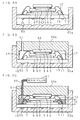
- FIGS. 2A and 2B are schematic cross-sectional views showing the structure of the optical device module according to the present invention.
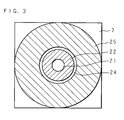
- FIG. 3 is a plan view showing the appearance of the optical device module according to the present invention.
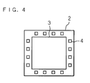
- FIG. 4 is a plan view showing a solid-state image sensor of the optical device module according to the present invention.
- FIG. 2A shows a condition in which an optical path delimiter is not fixed to an image sensing unit of the optical device module.
- FIG. 2B shows a condition in which the optical path delimiter is fixed.
- reference numeral 1 represents an image sensing unit having a solid-state image sensor 2 that receives external light
- reference numeral 20 represents an optical path delimiter having a lens 21.
- the image sensing unit 1 and the optical path delimiter 20 are separately fabricated, and thereafter, the optical path delimiter 20 is fixed to the image sensing unit 1 to thereby fabricate the optical device module.
- the image sensing unit 1 includes the solid-state image sensor 2, a transparent lid 6 protecting the solid-state image sensor 2, and a DSP 8 serving as a signal processor. These are placed one on another on a wiring board 7.
- the solid-state image sensor 2 is formed by applying a semiconductor process technology to a semiconductor board such as silicon.
- a pixel area 3 for performing photoelectric conversion On the solid-state image sensor 2, the following are formed: a pixel area 3 for performing photoelectric conversion; and a plurality of bonding pads 4 serving as connection terminals for connection to external circuits, input and output of electric signals and supply of power.
- the transparent lid 6 On the surface of the solid-state image sensor 2 where the pixel area 3 is formed, the transparent lid 6 is bonded by a bonding portion 5 so as to be opposed to the pixel area 3.
- the bonding portion 5 has a substantially rectangular shape surrounding the perimeter of the pixel area 3, and bonds the substantially rectangular transparent lid 6 to the solid-state image sensor 2 so that the space between the pixel area 3 and the transparent lid 6 is enclosed.
- the transparent lid 6 has a rectangular plate form, and is , made of a transparent material such as glass.
- the solid-state image sensor 2 captures the external incident light having passed through the transparent lid 6, and receives it by a plurality of light receiving elements arranged on the pixel area 3. Since an infrared intercepting film is applied to a surface of the transparent 6, the transparent lid 6 has the function of intercepting external infrared light.
- the bonding portion 5, which has a sheet-form bonding agent attached thereto, is formed by patterning by performing processing such as exposure or development by the photolithography technology. Since the photolithography technology is used, the patterning of the bonding portion 5 can be performed with high accuracy. Since a sheet-form bonding agent is used, the thickness of the bonding portion 5 can be made uniform. Whereby, the transparent lid 6 can be bonded to the pixel area 3 with high accuracy.
- the solid-state image sensor 2 to which the transparent lid 6 is bonded is placed, together with the DSP 8, on the wiring board 7 where a conductor wiring 11 is formed by patterning.
- the structure of the lamination is such that the DSP 8 is bonded onto the wiring board 7, a spacer 9 as which a rectangular-plate-form silicon piece is used is bonded onto the DSP 8 and the solid-state image sensor 2 is bonded onto the spacer 9.
- the DSP 8 is a semiconductor chip that controls the operation of the solid-state image sensor 2 and processes the signals outputted from the solid-state image sensor 2.
- a plurality of bonding pads (not shown) for performing input and output of electric signals and the like are formed on a surface of the DSP 8. After the DSP 8 is bonded onto the wiring board 7, the bonding pads of the DSP 8 and the conductor wiring 11 of the wiring board 7 are electrically connected together by bonding wires 13.
- the bonding pads 4 of the solid-state image sensor 2 bonded onto the spacer 9 and the conductor wiring 11 on the wiring board 7 are electrically connected together by bonding wires 12. Since the DSP 8 and the solid-state image sensor 2 are electrically connected together through the conductor wiring 11 on the wiring board 7, transmission and reception of electric signals can be performed therebetween. In order that the bonding wires 12 are out of contact with the DSP 8 or the bonding wires 13, the distance between the solid-state image sensor 2 and the DSP 8 is adjusted by the spacer 9.
- a sealing portion 14 made of a resin is formed substantially in the shape of a solid right circular cylinder on the wiring board 7, and the upper surface and approximately half of the transparent lid 6 protrude from the upper surface of the sealing portion 14.
- a screw portion 15 is provided on the side surface of the sealing portion 14, so that the image sensing unit 1 functions as a male screw.
- connection terminals 10 for , performing input and output of signals between the optical device module and digital cameras, camera phones or the like provided with the optical device module are provided in a protruding condition on the lower surface of the wiring board 7.
- the connection terminals 10 are electrically connected to the conductor wiring 11 formed on the upper surface of the wiring board 7.
- the optical path delimiter 20 for directing the external light to the pixel area 3 of the solid-state image sensor 2 includes the lens 21, a lens barrel 22 serving as the holder holding the lens 21, and a supporter 25 supporting the lens barrel 22 through an elastic material 24. While the lens barrel 22 has the shape of a cylinder in the figures, it may have the shape of a rectangular parallelepiped.
- the lens 21 is fixed to the inner surface of the lens barrel 22 so that the axial center of the lens barrel 22 and the optical axis of the lens 21 coincide with each other.
- the positioning claws 23 are arranged at regular intervals along the circumference on one end of the lens barrel 22.
- the positioning claws 23 determine the relative positions of the lens barrel 22 and the transparent lid 6 with respect to the direction of the plane of the transparent lid 6.
- the positioning claws 23 protrude in the axial direction from the side of the end of the lens barrel 22 to the outside of the end surface of the lens barrel 22.
- the disk-shaped elastic material 24 is fixed substantially in the center of the periphery of the lens barrel 22.
- the optical path delimiter 20 has the supporter 25 that supports the lens barrel 22 through the elastic material 24.
- the supporter 25 has a substantially circular through hole 26 vertically passing through the supporter 25.
- the through hole 26 includes two interconnected holes 26a and 26b having different inner diameters.
- the diameter of the upper hole 26a of the through hole 26 is larger than that of the lens barrel 22.
- a groove 27 where the diameter is larger than the inner diameter of the hole 26 is formed on the inner surface of the hole 26a.
- the elastic material 24 fixed to the lens barrel 22 is inserted in the groove 27 to thereby support the lens barrel 22 in the hole 26a of the supporter 25 through the elastic material 24. Since the groove 27 is slightly larger than the elastic material 24, the lens barrel 22 and the elastic material 24 can be slightly moved within the hole 26a in the direction of the axial center of the through hole 26 and the direction of the plane perpendicular to the axial center.
- a screw hole portion 28 to be engaged with the screw portion 15 is provided so that the optical path delimiter 20 functions as a female screw.
- the screw portion 15 provided on the image sensing unit 1 (the sealing portion 14) and the screw hole portion 28 provided on the optical path delimiter 20 (the supporter 25) are engaged together to thereby fix the image sensing unit 1 and the optical path delimiter 20.
- the screw portion 15 of the image sensing unit 1 and the screw hole portion 28 of the optical path delimiter 20 are engaged together to thereby fix the image sensing unit 1 and the optical path delimiter 20
- the image sensing unit 1 and the optical path delimiter 20 are fixed so that the upper surface of the sealing portion 14 of the image sensing unit 1 and the lower surface of the supporter 25 of the optical path delimiter 20 are in contact with each other.
- the lower end surface of the lens barrel 22 is in contact with the upper surface of the transparent lid 6 and the positioning claws 23 abut on the periphery of the transparent lid 6 from four directions to thereby fix the relative positions of the lens barrel 22 and the transparent lid 6.
- the positioning claws 23 of the lens barrel 22 are out of contact with the upper surface of the sealing portion 14 when the lens barrel 22 is fixed to the transparent lid 6, the diameter of the opening at the lower end of the hole 26a is larger than the inner diameter of the hole 26a, and the lower surface of the supporter 25 is out of contact with the transparent lid 6 and the positioning claws 23.
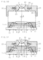
- FIGS. 5A to 5F are schematic views showing the fabrication process of the optical device module according to the present invention.
- FIGS. 5A, 5B and 5C show a process to seal the image sensing unit 1 in the resin.
- FIGS. 5D, 5E and 5F show a process to fix the optical path delimiter 20 to the image sensing unit 1.
- the DSP 8, the solid-state image sensor 2 and the like placed one on another on the wiring board 7 are placed into a container 50a to be filled with the resin (FIG. 5A).
- the size of the bottom surface inside the container 50a is substantially the same as that of the wiring board 7.
- a plurality of hemispherical concave portions 53 for accommodating the disposed connection terminals 10 are formed on the lower surface of the wiring board 7 so that the bottom surface inside the container 50a and the lower surface of the wiring board 7 are in close contact with each other.
- the resin is prevented from flowing to the lower surface of the wiring board 7 by making the , bottom surface inside the container 50a and the lower surface of the wiring board 7 in close contact with each other.
- a lid 50b is inserted along the inner surface of the container 50a to constitute a mold, and the space within the mold is enclosed.
- the lid 50b has an inlet 51 for filling the resin, and the inside of the mold communicates with the outside only through the inlet 51 (FIG. 5B).
- Female screw grooves 54 are formed on the leg portion of the lid 50b.
- a cylindrical filling pipe 60 is inserted in the inlet 51, and the resin is filled into the mold through the filling pipe 60 by a resin filler 61 (FIG. 5C). Then, the resin cures, so that the sealing portion 14 having the screw portion 15 on its side surface is formed in the image sensing unit 1.
- a concave portion 52 for accommodating an upper part of the transparent lid 6 may be formed on the upper surface inside the lid 50b as shown in the figure.
- the sealing portion 14 can be formed so that the upper part of the transparent lid 6 accommodated in the concave portion 52 is always exposed out of the upper surface of the sealing portion 14 even when a resin of an amount larger than the volume of the space of the mold is filled. It is to be noted that the height Z of the sealing portion 14 may be adjusted by controlling the filling amount of the resin.
- the optical path delimiter 20 fabricated separately is fixed to the image sensing unit 1.
- the engagement of the screw portion 15 of the image sensing unit 1 and the screw hole portion 28 of the optical path delimiter 20 is started (FIG. 5D).
- the transparent lid 6 of the image sensing unit 1 and the positioning claws 23 of the optical path delimiter 20 are not engaged with each other.
- the optical axis of the lens 21 and the optical center of the pixel area of the solid-state image sensor 2 may disaccord with each other (A ⁇ 0), and they rarely coincide with each other because of the manufacturing nonuniformity.
- FIG. 5E shows a condition where the left positioning claws 23 are in contact with the transparent lid 6.
- the relative position of the lens barrel 22 with respect to the transparent lid 6 automatically moves in a direction where the optical axis of the lens 21 and the optical center of the pixel area of the solid-state image sensor 2 coincide with each other, the lens barrel 22 is fixed by being pressed against the transparent lid 6 by the elastic material 24, and the supporter 5 is fixed to the image sensing unit 1 by the screw portion 15 and the screw hole portion 28 so as to be immovable (FIG., 5F).
- the transparent lid 6 moves along the ridgeline of the positioning claws 23 by the pressing, the optical axis of the lens 21 and the optical center of the pixel area 3 of the solid-state image sensor 2 can be made to coincide with each other.
- the configuration of the ridgeline of the positioning claws 23 is appropriately determined in consideration of the manufacturing nonuniformity.
- the distance between the pixel area 3 of the solid-state image sensor 2 and the lens 21 is uniquely determined by the sum total of the thickness of the bonding portion 5 and the transparent lid 6 and the distance from the lower end of the lens barrel 22 to the part where the lens 21 is fixed. Since the positioning claws 23 of the lens barrel 22 abut on the periphery of the transparent lid 6 from four directions to thereby fix the relative positions, the position of the lens 21 in the direction of the plane of the transparent lid 6 is uniquely determined. Since the transparent lid 6 is bonded while highly accurately positioned with respect to the pixel area 3 of the solid-state image sensor 2, the lens barrel 22 can be fixed while highly accurately positioned with respect to the pixel area 3 with reference to the transparent lid 6.
- the solid-state image sensor 2, the DSP 8 and the like of the image sensing unit 1 are sealed in a resin, these can be protected from external shocks, and the manufacturing process is easy. Since the lens barrel 22 of the optical path delimiter 20 is supported by the supporter 25 through the elastic material 24 and the elastic material 24 is movable within the groove 27 of the supporter 25, the lens barrel 22 and the supporter 25 can be fixed to the image sensing unit 1 by different procedures, and the position of the lens 21 can be fixed with respect to the solid-state image sensor 2 without affected by a configuration error of the sealing portion 14 and the supporter 25.
- the lens barrel 22 of the optical path delimiter 20 has the positioning claws 23 in the present embodiment, it may be provided with no positioning claw 23. In this case, the positioning in the direction of the plane is performed in the process to bring the lower surface of the lens barrel 22 into contact with the upper surface of the transparent lid 6, and thereafter, the supporter 5 is fixed to the image sensing unit 1.
- the solid-state image sensor 2 and the DSP 8 serving as the signal processor are placed one on another as separate semiconductor chips, they may be formed as one semiconductor chip.
- a semiconductor chip other than the DSP 8 may be placed together with the solid-state image sensor 2. Further, a multiplicity of semiconductor chips may be placed one on another.
- the shape of the mold for the sealing in a synthetic resin is merely an example, and the present invention is not limited thereto.
Landscapes
- Engineering & Computer Science (AREA)
- Multimedia (AREA)
- Signal Processing (AREA)
- Transforming Light Signals Into Electric Signals (AREA)
- Solid State Image Pick-Up Elements (AREA)
- Camera Bodies And Camera Details Or Accessories (AREA)
- Studio Devices (AREA)
- Lens Barrels (AREA)
Applications Claiming Priority (1)
| Application Number | Priority Date | Filing Date | Title |
|---|---|---|---|
| JP2005103775A JP4233536B2 (ja) | 2005-03-31 | 2005-03-31 | 光学装置用モジュール |
Publications (2)
| Publication Number | Publication Date |
|---|---|
| EP1708476A2 true EP1708476A2 (de) | 2006-10-04 |
| EP1708476A3 EP1708476A3 (de) | 2008-01-16 |
Family
ID=36676455
Family Applications (1)
| Application Number | Title | Priority Date | Filing Date |
|---|---|---|---|
| EP06251791A Withdrawn EP1708476A3 (de) | 2005-03-31 | 2006-03-30 | Optisches Bauelement-Modul |
Country Status (6)
| Country | Link |
|---|---|
| US (1) | US7294828B2 (de) |
| EP (1) | EP1708476A3 (de) |
| JP (1) | JP4233536B2 (de) |
| KR (1) | KR100758584B1 (de) |
| CN (1) | CN100423562C (de) |
| TW (1) | TWI302209B (de) |
Cited By (3)
| Publication number | Priority date | Publication date | Assignee | Title |
|---|---|---|---|---|
| EP2857896A3 (de) * | 2013-09-12 | 2015-08-19 | Sunming Technologies (HK) Limited | Staubfreie Linsensteuerungsvorrichtung |
| EP3108505A4 (de) * | 2014-02-18 | 2017-11-15 | Heptagon Micro Optics Pte. Ltd. | Optische module mit anpassbaren abstandshaltern zur brennweitenanpassung und/oder reduktion der neigung sowie herstellung der optischen module |
| US10764479B2 (en) | 2013-08-08 | 2020-09-01 | Sony Corporation | Imaging apparatus, manufacturing apparatus, manufacturing method and electronic appliance |
Families Citing this family (37)
| Publication number | Priority date | Publication date | Assignee | Title |
|---|---|---|---|---|
| US7127793B2 (en) * | 2002-04-24 | 2006-10-31 | Fuji Photo Film Co., Ltd. | Method of producing solid state pickup device |
| JP2006276463A (ja) * | 2005-03-29 | 2006-10-12 | Sharp Corp | 光学装置用モジュール及び光学装置用モジュールの製造方法 |
| CN1885909A (zh) * | 2005-06-24 | 2006-12-27 | 鸿富锦精密工业(深圳)有限公司 | 数码相机模块 |
| DE102005059161A1 (de) * | 2005-12-12 | 2007-06-21 | Robert Bosch Gmbh | Optisches Modul sowie Verfahren zur Montage eines optischen Moduls |
| KR100770690B1 (ko) * | 2006-03-15 | 2007-10-29 | 삼성전기주식회사 | 카메라모듈 패키지 |
| JP4189769B2 (ja) * | 2006-10-18 | 2008-12-03 | 進展産業株式会社 | 撮像装置 |
| US20080118241A1 (en) * | 2006-11-16 | 2008-05-22 | Tekolste Robert | Control of stray light in camera systems employing an optics stack and associated methods |
| JP4340698B2 (ja) | 2007-04-27 | 2009-10-07 | シャープ株式会社 | 光学ユニットおよびそれを備えた固体撮像装置並びに電子機器 |
| JP4324623B2 (ja) * | 2007-04-27 | 2009-09-02 | シャープ株式会社 | 固体撮像装置およびそれを備えた電子機器 |
| KR101366251B1 (ko) * | 2007-05-28 | 2014-02-21 | 삼성전자주식회사 | 전자기기의 충격 흡수 장치 |
| US20100259655A1 (en) * | 2007-11-01 | 2010-10-14 | Konica Minolta Holdings, Inc. | Imaging device |
| US9118825B2 (en) * | 2008-02-22 | 2015-08-25 | Nan Chang O-Film Optoelectronics Technology Ltd. | Attachment of wafer level optics |
| JP2009204721A (ja) * | 2008-02-26 | 2009-09-10 | Fujinon Corp | カメラモジュール及びカメラモジュールの実装方法 |
| CN101592772A (zh) * | 2008-05-27 | 2009-12-02 | 鸿富锦精密工业(深圳)有限公司 | 镜头装置、用于收容该镜头装置的电子装置及摄像设备 |
| JP5498684B2 (ja) * | 2008-11-07 | 2014-05-21 | ラピスセミコンダクタ株式会社 | 半導体モジュール及びその製造方法 |
| US8654215B2 (en) | 2009-02-23 | 2014-02-18 | Gary Edwin Sutton | Mobile communicator with curved sensor camera |
| US8248499B2 (en) * | 2009-02-23 | 2012-08-21 | Gary Edwin Sutton | Curvilinear sensor system |
| US9419032B2 (en) | 2009-08-14 | 2016-08-16 | Nanchang O-Film Optoelectronics Technology Ltd | Wafer level camera module with molded housing and method of manufacturing |
| CN102036004B (zh) * | 2009-09-30 | 2013-07-03 | 鸿富锦精密工业(深圳)有限公司 | 成像模组 |
| JP5261548B2 (ja) | 2011-07-29 | 2013-08-14 | シャープ株式会社 | カメラモジュール |
| EP2814063B1 (de) * | 2012-02-07 | 2019-12-04 | Nikon Corporation | Bildgebungseinheit und bildgebungsvorrichtung |
| US20130271790A1 (en) * | 2012-04-14 | 2013-10-17 | Shinten Sangyo Co., Ltd. | Imaging Module Unit for Copier |
| DE102012210818A1 (de) * | 2012-06-26 | 2014-01-02 | Robert Bosch Gmbh | Kameramodul für ein Fahrzeug und Verfahren zu dessen Herstellung |
| JP6268856B2 (ja) * | 2013-09-24 | 2018-01-31 | 三菱電機株式会社 | 光モジュールおよびその製造方法 |
| JP6197538B2 (ja) * | 2013-09-27 | 2017-09-20 | 三菱電機株式会社 | 光モジュール、光モジュール用レンズキャップ |
| EP2887637B1 (de) * | 2013-12-19 | 2015-11-04 | Axis AB | Bildkollektorvorrichtung mit abgedichtetem Sensorraum und Verfahren zum Abdichten eines Sensorraums in einer Bildkollektorvorrichtung |
| US20160307881A1 (en) * | 2015-04-20 | 2016-10-20 | Advanced Semiconductor Engineering, Inc. | Optical sensor module and method for manufacturing the same |
| US9769361B2 (en) * | 2015-08-31 | 2017-09-19 | Adlink Technology Inc. | Assembly structure for industrial cameras |
| US10750071B2 (en) * | 2016-03-12 | 2020-08-18 | Ningbo Sunny Opotech Co., Ltd. | Camera module with lens array arrangement, circuit board assembly, and image sensor and manufacturing method thereof |
| EP3468165B1 (de) * | 2016-03-28 | 2023-12-20 | Ningbo Sunny Opotech Co., Ltd. | Kameramodul und geformte lichtempfindliche anordnung sowie herstellungsverfahren dafür und elektronische vorrichtung |
| CN109716745B (zh) * | 2016-08-01 | 2020-12-18 | 宁波舜宇光电信息有限公司 | 摄像模组及其模塑电路板组件和模塑感光组件和制造方法 |
| US20180315894A1 (en) * | 2017-04-26 | 2018-11-01 | Advanced Semiconductor Engineering, Inc. | Semiconductor device package and a method of manufacturing the same |
| TWI647828B (zh) | 2017-07-10 | 2019-01-11 | Azurewave Technologies, Inc. | 可攜式電子裝置及其影像擷取模組與影像感測組件 |
| TWI699118B (zh) * | 2017-09-11 | 2020-07-11 | 大陸商寧波舜宇光電信息有限公司 | 攝像模組及其感光元件、電子設備、成型模具和製造方法 |
| CN207184660U (zh) * | 2017-09-15 | 2018-04-03 | 南昌欧菲光电技术有限公司 | 摄像模组 |
| KR102050739B1 (ko) * | 2017-09-27 | 2019-12-02 | 최도영 | 카메라 모듈 |
| JP7725586B2 (ja) * | 2021-06-24 | 2025-08-19 | 京セラ株式会社 | 非接触通信媒体 |
Family Cites Families (15)
| Publication number | Priority date | Publication date | Assignee | Title |
|---|---|---|---|---|
| NL1003315C2 (nl) * | 1996-06-11 | 1997-12-17 | Europ Semiconductor Assembly E | Werkwijze voor het inkapselen van een geïntegreerde halfgeleiderschake- ling. |
| JP2002134725A (ja) * | 2000-10-23 | 2002-05-10 | Htt:Kk | 固体撮像装置 |
| KR100422040B1 (ko) | 2001-09-11 | 2004-03-11 | 삼성전기주식회사 | 촬상소자 모듈 패키지 |
| JP3787765B2 (ja) * | 2001-11-30 | 2006-06-21 | 松下電器産業株式会社 | 固体撮像装置およびその製造方法 |
| JP2003264274A (ja) * | 2002-03-11 | 2003-09-19 | Seiko Instruments Inc | カメラモジュール |
| JP4061936B2 (ja) * | 2002-03-22 | 2008-03-19 | コニカミノルタホールディングス株式会社 | 撮像装置 |
| JP4285966B2 (ja) * | 2002-09-27 | 2009-06-24 | 三洋電機株式会社 | カメラモジュール |
| US6940058B2 (en) * | 2003-02-04 | 2005-09-06 | Kingpak Technology, Inc. | Injection molded image sensor module |
| JP2004296453A (ja) | 2003-02-06 | 2004-10-21 | Sharp Corp | 固体撮像装置、半導体ウエハ、光学装置用モジュール、固体撮像装置の製造方法及び光学装置用モジュールの製造方法 |
| JP3768487B2 (ja) | 2003-03-26 | 2006-04-19 | 三菱電機株式会社 | カメラモジュール |
| JP4204368B2 (ja) | 2003-03-28 | 2009-01-07 | シャープ株式会社 | 光学装置用モジュール及び光学装置用モジュールの製造方法 |
| US7199438B2 (en) * | 2003-09-23 | 2007-04-03 | Advanced Semiconductor Engineering, Inc. | Overmolded optical package |
| US6870208B1 (en) * | 2003-09-24 | 2005-03-22 | Kingpak Technology Inc. | Image sensor module |
| JP4446773B2 (ja) * | 2004-03-26 | 2010-04-07 | 富士フイルム株式会社 | 撮影装置 |
| JP2004266844A (ja) * | 2004-03-26 | 2004-09-24 | Mitsubishi Electric Corp | 撮像装置及びその製造方法 |
-
2005
- 2005-03-31 JP JP2005103775A patent/JP4233536B2/ja not_active Expired - Fee Related
-
2006
- 2006-03-30 EP EP06251791A patent/EP1708476A3/de not_active Withdrawn
- 2006-03-30 US US11/396,427 patent/US7294828B2/en not_active Expired - Fee Related
- 2006-03-30 TW TW095111290A patent/TWI302209B/zh not_active IP Right Cessation
- 2006-03-31 KR KR1020060029824A patent/KR100758584B1/ko not_active Expired - Fee Related
- 2006-03-31 CN CNB2006100719797A patent/CN100423562C/zh not_active Expired - Fee Related
Cited By (7)
| Publication number | Priority date | Publication date | Assignee | Title |
|---|---|---|---|---|
| US10764479B2 (en) | 2013-08-08 | 2020-09-01 | Sony Corporation | Imaging apparatus, manufacturing apparatus, manufacturing method and electronic appliance |
| US11483456B2 (en) | 2013-08-08 | 2022-10-25 | Sony Corporation | Imaging apparatus, manufacturing apparatus, manufacturing method and electronic appliance |
| US11856279B2 (en) | 2013-08-08 | 2023-12-26 | Sony Group Corporation | Imaging apparatus, manufacturing apparatus, manufacturing method and electronic appliance |
| EP2857896A3 (de) * | 2013-09-12 | 2015-08-19 | Sunming Technologies (HK) Limited | Staubfreie Linsensteuerungsvorrichtung |
| EP3108505A4 (de) * | 2014-02-18 | 2017-11-15 | Heptagon Micro Optics Pte. Ltd. | Optische module mit anpassbaren abstandshaltern zur brennweitenanpassung und/oder reduktion der neigung sowie herstellung der optischen module |
| US9887221B2 (en) | 2014-02-18 | 2018-02-06 | Heptagon Micro Optics Pte. Ltd. | Optical modules including customizable spacers for focal length adjustment and/or reduction of tilt, and fabrication of the optical modules |
| US10204945B2 (en) | 2014-02-18 | 2019-02-12 | Heptagon Micro Optics Pte. Ltd. | Optical modules including customizable spacers for focal length adjustment and/or reduction of tilt, and fabrication of the optical modules |
Also Published As
| Publication number | Publication date |
|---|---|
| TW200641430A (en) | 2006-12-01 |
| CN1842139A (zh) | 2006-10-04 |
| US20060219885A1 (en) | 2006-10-05 |
| CN100423562C (zh) | 2008-10-01 |
| JP4233536B2 (ja) | 2009-03-04 |
| TWI302209B (en) | 2008-10-21 |
| EP1708476A3 (de) | 2008-01-16 |
| KR100758584B1 (ko) | 2007-09-13 |
| JP2006287533A (ja) | 2006-10-19 |
| US7294828B2 (en) | 2007-11-13 |
| KR20060105677A (ko) | 2006-10-11 |
Similar Documents
| Publication | Publication Date | Title |
|---|---|---|
| US7294828B2 (en) | Distortion and shock resistant optical device module for image capture | |
| KR100779119B1 (ko) | 광학장치용 모듈, 광로획정기, 및 광학장치용 모듈의제조방법 | |
| US7397023B2 (en) | Image sensor module with optical path delimiter and accurate alignment | |
| TWI273300B (en) | Module for optical device, and manufacturing method therefor | |
| KR102282687B1 (ko) | 일체형 패키징 공정 기반 카메라 모듈, 그 일체형 기저 부품 및 그 제조 방법 | |
| TWI392337B (zh) | 晶圓為主之攝影機模組及其製造方法 | |
| KR100822968B1 (ko) | 광학 장치용 모듈 및 광학 장치용 모듈의 제조 방법 | |
| US7848639B2 (en) | Solid-state image sensing device and electronic apparatus comprising same | |
| KR100730726B1 (ko) | 카메라 모듈 | |
| JP4248586B2 (ja) | 撮像装置及びその製造方法、並びに該撮像装置を搭載した携帯情報端末及び撮像機器 | |
| KR20200063105A (ko) | 촬영 어셈블리 및 이의 패키징 방법, 렌즈 모듈, 전자 기기 | |
| KR20200063107A (ko) | 촬영 어셈블리 및 이의 패키징 방법, 렌즈 모듈, 전자 기기 | |
| CN109672806B (zh) | 摄像模组和感光组件及其封装方法 | |
| KR101051533B1 (ko) | 카메라 모듈 | |
| US20050237419A1 (en) | Camera module, holder for use in a camera module, camera system and method of manufacturing a camera module | |
| KR20200063106A (ko) | 촬영 어셈블리 및 이의 패키징 방법, 렌즈 모듈, 전자 기기 |
Legal Events
| Date | Code | Title | Description |
|---|---|---|---|
| PUAI | Public reference made under article 153(3) epc to a published international application that has entered the european phase |
Free format text: ORIGINAL CODE: 0009012 |
|
| AK | Designated contracting states |
Kind code of ref document: A2 Designated state(s): AT BE BG CH CY CZ DE DK EE ES FI FR GB GR HU IE IS IT LI LT LU LV MC NL PL PT RO SE SI SK TR |
|
| AX | Request for extension of the european patent |
Extension state: AL BA HR MK YU |
|
| PUAL | Search report despatched |
Free format text: ORIGINAL CODE: 0009013 |
|
| AK | Designated contracting states |
Kind code of ref document: A3 Designated state(s): AT BE BG CH CY CZ DE DK EE ES FI FR GB GR HU IE IS IT LI LT LU LV MC NL PL PT RO SE SI SK TR |
|
| AX | Request for extension of the european patent |
Extension state: AL BA HR MK YU |
|
| AKX | Designation fees paid | ||
| REG | Reference to a national code |
Ref country code: DE Ref legal event code: 8566 |
|
| STAA | Information on the status of an ep patent application or granted ep patent |
Free format text: STATUS: THE APPLICATION IS DEEMED TO BE WITHDRAWN |
|
| 18D | Application deemed to be withdrawn |
Effective date: 20080717 |