EP1710734A2 - Etiquette RFID - Google Patents
Etiquette RFID Download PDFInfo
- Publication number
- EP1710734A2 EP1710734A2 EP05255481A EP05255481A EP1710734A2 EP 1710734 A2 EP1710734 A2 EP 1710734A2 EP 05255481 A EP05255481 A EP 05255481A EP 05255481 A EP05255481 A EP 05255481A EP 1710734 A2 EP1710734 A2 EP 1710734A2
- Authority
- EP
- European Patent Office
- Prior art keywords
- pattern
- conductive pattern
- rfid tag
- antenna
- peeling detection
- Prior art date
- Legal status (The legal status is an assumption and is not a legal conclusion. Google has not performed a legal analysis and makes no representation as to the accuracy of the status listed.)
- Withdrawn
Links
Images



Classifications
-
- G—PHYSICS
- G06—COMPUTING OR CALCULATING; COUNTING
- G06K—GRAPHICAL DATA READING; PRESENTATION OF DATA; RECORD CARRIERS; HANDLING RECORD CARRIERS
- G06K19/00—Record carriers for use with machines and with at least a part designed to carry digital markings
- G06K19/06—Record carriers for use with machines and with at least a part designed to carry digital markings characterised by the kind of the digital marking, e.g. shape, nature, code
- G06K19/067—Record carriers with conductive marks, printed circuits or semiconductor circuit elements, e.g. credit or identity cards also with resonating or responding marks without active components
- G06K19/07—Record carriers with conductive marks, printed circuits or semiconductor circuit elements, e.g. credit or identity cards also with resonating or responding marks without active components with integrated circuit chips
-
- G—PHYSICS
- G06—COMPUTING OR CALCULATING; COUNTING
- G06K—GRAPHICAL DATA READING; PRESENTATION OF DATA; RECORD CARRIERS; HANDLING RECORD CARRIERS
- G06K19/00—Record carriers for use with machines and with at least a part designed to carry digital markings
- G06K19/06—Record carriers for use with machines and with at least a part designed to carry digital markings characterised by the kind of the digital marking, e.g. shape, nature, code
- G06K19/067—Record carriers with conductive marks, printed circuits or semiconductor circuit elements, e.g. credit or identity cards also with resonating or responding marks without active components
- G06K19/07—Record carriers with conductive marks, printed circuits or semiconductor circuit elements, e.g. credit or identity cards also with resonating or responding marks without active components with integrated circuit chips
- G06K19/077—Constructional details, e.g. mounting of circuits in the carrier
- G06K19/07749—Constructional details, e.g. mounting of circuits in the carrier the record carrier being capable of non-contact communication, e.g. constructional details of the antenna of a non-contact smart card
- G06K19/0775—Constructional details, e.g. mounting of circuits in the carrier the record carrier being capable of non-contact communication, e.g. constructional details of the antenna of a non-contact smart card arrangements for connecting the integrated circuit to the antenna
-
- G—PHYSICS
- G06—COMPUTING OR CALCULATING; COUNTING
- G06K—GRAPHICAL DATA READING; PRESENTATION OF DATA; RECORD CARRIERS; HANDLING RECORD CARRIERS
- G06K19/00—Record carriers for use with machines and with at least a part designed to carry digital markings
- G06K19/06—Record carriers for use with machines and with at least a part designed to carry digital markings characterised by the kind of the digital marking, e.g. shape, nature, code
- G06K19/067—Record carriers with conductive marks, printed circuits or semiconductor circuit elements, e.g. credit or identity cards also with resonating or responding marks without active components
- G06K19/07—Record carriers with conductive marks, printed circuits or semiconductor circuit elements, e.g. credit or identity cards also with resonating or responding marks without active components with integrated circuit chips
- G06K19/073—Special arrangements for circuits, e.g. for protecting identification code in memory
-
- G—PHYSICS
- G06—COMPUTING OR CALCULATING; COUNTING
- G06K—GRAPHICAL DATA READING; PRESENTATION OF DATA; RECORD CARRIERS; HANDLING RECORD CARRIERS
- G06K19/00—Record carriers for use with machines and with at least a part designed to carry digital markings
- G06K19/06—Record carriers for use with machines and with at least a part designed to carry digital markings characterised by the kind of the digital marking, e.g. shape, nature, code
- G06K19/067—Record carriers with conductive marks, printed circuits or semiconductor circuit elements, e.g. credit or identity cards also with resonating or responding marks without active components
- G06K19/07—Record carriers with conductive marks, printed circuits or semiconductor circuit elements, e.g. credit or identity cards also with resonating or responding marks without active components with integrated circuit chips
- G06K19/073—Special arrangements for circuits, e.g. for protecting identification code in memory
- G06K19/07309—Means for preventing undesired reading or writing from or onto record carriers
- G06K19/07372—Means for preventing undesired reading or writing from or onto record carriers by detecting tampering with the circuit
- G06K19/07381—Means for preventing undesired reading or writing from or onto record carriers by detecting tampering with the circuit with deactivation or otherwise incapacitation of at least a part of the circuit upon detected tampering
-
- G—PHYSICS
- G06—COMPUTING OR CALCULATING; COUNTING
- G06K—GRAPHICAL DATA READING; PRESENTATION OF DATA; RECORD CARRIERS; HANDLING RECORD CARRIERS
- G06K19/00—Record carriers for use with machines and with at least a part designed to carry digital markings
- G06K19/06—Record carriers for use with machines and with at least a part designed to carry digital markings characterised by the kind of the digital marking, e.g. shape, nature, code
- G06K19/067—Record carriers with conductive marks, printed circuits or semiconductor circuit elements, e.g. credit or identity cards also with resonating or responding marks without active components
- G06K19/07—Record carriers with conductive marks, printed circuits or semiconductor circuit elements, e.g. credit or identity cards also with resonating or responding marks without active components with integrated circuit chips
- G06K19/073—Special arrangements for circuits, e.g. for protecting identification code in memory
- G06K19/07309—Means for preventing undesired reading or writing from or onto record carriers
- G06K19/07372—Means for preventing undesired reading or writing from or onto record carriers by detecting tampering with the circuit
- G06K19/07381—Means for preventing undesired reading or writing from or onto record carriers by detecting tampering with the circuit with deactivation or otherwise incapacitation of at least a part of the circuit upon detected tampering
- G06K19/0739—Means for preventing undesired reading or writing from or onto record carriers by detecting tampering with the circuit with deactivation or otherwise incapacitation of at least a part of the circuit upon detected tampering the incapacitated circuit being part of an antenna
-
- G—PHYSICS
- G06—COMPUTING OR CALCULATING; COUNTING
- G06K—GRAPHICAL DATA READING; PRESENTATION OF DATA; RECORD CARRIERS; HANDLING RECORD CARRIERS
- G06K19/00—Record carriers for use with machines and with at least a part designed to carry digital markings
- G06K19/06—Record carriers for use with machines and with at least a part designed to carry digital markings characterised by the kind of the digital marking, e.g. shape, nature, code
- G06K19/067—Record carriers with conductive marks, printed circuits or semiconductor circuit elements, e.g. credit or identity cards also with resonating or responding marks without active components
- G06K19/07—Record carriers with conductive marks, printed circuits or semiconductor circuit elements, e.g. credit or identity cards also with resonating or responding marks without active components with integrated circuit chips
- G06K19/077—Constructional details, e.g. mounting of circuits in the carrier
-
- G—PHYSICS
- G06—COMPUTING OR CALCULATING; COUNTING
- G06K—GRAPHICAL DATA READING; PRESENTATION OF DATA; RECORD CARRIERS; HANDLING RECORD CARRIERS
- G06K19/00—Record carriers for use with machines and with at least a part designed to carry digital markings
- G06K19/06—Record carriers for use with machines and with at least a part designed to carry digital markings characterised by the kind of the digital marking, e.g. shape, nature, code
- G06K19/067—Record carriers with conductive marks, printed circuits or semiconductor circuit elements, e.g. credit or identity cards also with resonating or responding marks without active components
- G06K19/07—Record carriers with conductive marks, printed circuits or semiconductor circuit elements, e.g. credit or identity cards also with resonating or responding marks without active components with integrated circuit chips
- G06K19/077—Constructional details, e.g. mounting of circuits in the carrier
- G06K19/07749—Constructional details, e.g. mounting of circuits in the carrier the record carrier being capable of non-contact communication, e.g. constructional details of the antenna of a non-contact smart card
-
- H—ELECTRICITY
- H10—SEMICONDUCTOR DEVICES; ELECTRIC SOLID-STATE DEVICES NOT OTHERWISE PROVIDED FOR
- H10W—GENERIC PACKAGES, INTERCONNECTIONS, CONNECTORS OR OTHER CONSTRUCTIONAL DETAILS OF DEVICES COVERED BY CLASS H10
- H10W72/00—Interconnections or connectors in packages
- H10W72/071—Connecting or disconnecting
- H10W72/072—Connecting or disconnecting of bump connectors
- H10W72/07251—Connecting or disconnecting of bump connectors characterised by changes in properties of the bump connectors during connecting
-
- H—ELECTRICITY
- H10—SEMICONDUCTOR DEVICES; ELECTRIC SOLID-STATE DEVICES NOT OTHERWISE PROVIDED FOR
- H10W—GENERIC PACKAGES, INTERCONNECTIONS, CONNECTORS OR OTHER CONSTRUCTIONAL DETAILS OF DEVICES COVERED BY CLASS H10
- H10W72/00—Interconnections or connectors in packages
- H10W72/20—Bump connectors, e.g. solder bumps or copper pillars; Dummy bumps; Thermal bumps
-
- H—ELECTRICITY
- H10—SEMICONDUCTOR DEVICES; ELECTRIC SOLID-STATE DEVICES NOT OTHERWISE PROVIDED FOR
- H10W—GENERIC PACKAGES, INTERCONNECTIONS, CONNECTORS OR OTHER CONSTRUCTIONAL DETAILS OF DEVICES COVERED BY CLASS H10
- H10W90/00—Package configurations
- H10W90/701—Package configurations characterised by the relative positions of pads or connectors relative to package parts
- H10W90/721—Package configurations characterised by the relative positions of pads or connectors relative to package parts of bump connectors
- H10W90/724—Package configurations characterised by the relative positions of pads or connectors relative to package parts of bump connectors between a chip and a stacked insulating package substrate, interposer or RDL
Definitions
- the present invention relates to an RFID tag (Radio_Frequency_IDentification) tag which exchanges information with an external device in a non-contact manner.
- RFID tag Radio_Frequency_IDentification
- the "RFID tag” used in the present specification is regarded as an internal component (inlay) for the “RFID tag” and so it may be referred to as an "inlay for radio IC tag”. Or this "RFID tag” may be referred to as a "radio IC tag”.
- this "RFID tag” also includes a non-contact type IC card.
- Fig. 1 is a plan view showing an example of an RFID tag. The figure illustrates a state in which a cover sheet, etc. , is removed.
- an antenna pattern 12 is formed on a base sheet 11 and an IC chip 13 is placed on this antenna pattern 12.
- This antenna pattern 12 is a conductive pattern which operates as a dipole antenna consisting of two mono pole patterns 121, 122 extending sideward from the IC chip 13, ends on the IC chip 13 side of which are electrically connected to the IC chip 13. Furthermore, this antenna pattern 12 is provided with a correction pattern 123 for correction of an antenna characteristic, which bypasses the IC chip 13 and connects two extending sections (which correspond to the two mono pole patterns 121, 122 in the structure shown in this Fig. 1), one end of which is connected to the IC chip 13, of this antenna pattern 12.
- a circuit for carrying out a radio communication with an external device using the antenna pattern 12 as an antenna is built in this IC chip 13.
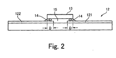
- Fig. 2 shows a connection structure between the IC chip 13 and antenna pattern 12.
- the IC chip 13 and antenna pattern 12 are connected by means of flip chip through bumps 14 and surroundings of the bumps 14 are fixed by an adhesive 15.
- the ends of the antenna pattern 12 and the IC chip 13 vertically overlap with each other in areas D shown in Fig. 2, which produces a parasitic capacitance C in those parts.
- this parasitic capacitance C causes an adverse influence on the antenna characteristic (radio communication characteristic).
- the correction pattern 123 shown in Fig. 1 operates as an inductor L which cancels out the influence of this parasitic capacitance C.
- the RFID tag 10 has the basic structure shown in Fig. 1, Fig. 2 and the antenna pattern 12 and circuit chip 13 are further covered with a cover sheet.
- Fig. 3 is a plan view showing an example of an RFID tag having the basic structure which has been explained with reference to Fig. 1, Fig. 2 and with a peeling detection function added. A cover such as a cover sheet is removed in this Fig. 3, too.
- an antenna pattern 12 made up of mono pole patterns 121, 122 as a dipole antenna is formed on a base sheet 11 and an IC chip 13 is connected to ends of the two mono pole patterns 121, 122 by means of flip chip. Furthermore, this antenna pattern 12 includes a correction pattern 123 which bypasses the IC chip 13 and connects the mono pole patterns 121, 122.
- a loop peeling detection pattern 16 is additionally formed on the base sheet 11 in such a way as to surround the antenna pattern 12. Both ends of the loop of this peeling detection pattern 16 are also connected to the IC chip 13 by means of flip chip in a structure similar to the connection structure (see Fig. 2) between the antenna pattern 12 and IC chip 13 and this IC chip 13 includes not only the function of radio communication with an external device using the antenna pattern 12 but also the function of detecting destruction of the peeling detection pattern 16.
- the peeling detection pattern 16 is made of a material such as silver paste, which is conductive, relatively brittle and destructible. This peeling detection pattern 16 is provided with peeling detection points 161 at several locations on the loop.
- the peeling detection pattern 16 is further covered with a cover sheet.
- the peeling detection points 161 of the peeling detection pattern 16 are strongly bonded to the cover sheet, while parts other than the peeling detection points 161 of the peeling detection pattern 16 are bonded more strongly to the base sheet 11 than to the cover sheet. For this reason, when an attempt is made to peel off the cover sheet, the cover sheet is peeled off with only the peeling detection points 161 of the peeling detection pattern 16 remaining bonded to the cover sheet, the peeling detection pattern 16 is destroyed and the IC chip 13 detects the destruction of the peeling detection pattern 16. This prevents the tampering of this RFID tag 10.
- the peeling detection pattern 16 surrounds the antenna pattern 12 and this peeling detection pattern is also made of a conductor, which produces an adverse effect on the antenna characteristic of the antenna pattern 12, greatly attenuates radio waves emitted from the antenna pattern 12 compared to a case in which the peeling detection pattern 16 does not exist (see Fig. 1), causing a problem that the outreach of radio waves (distance within which a radio communication is possible) is drastically shortened.
- the present invention has been made in view of the above circumstances and provides an RFID tag having a function of detecting peeling while maintaining good antenna characteristics.
- the RFID tag according to the present invention is provided with; a base; a first conductive pattern provided on the base, which operates as a communication antenna; a second conductive pattern for peeling detection provided on the base, which is destroyed when peeled off the base; a circuit chip electrically connected to both the first conductive pattern and the second conductive pattern, which carries out a radio communication using the first conductive pattern as an antenna and detects the destruction of the second conductive pattern; and a cover covering the first conductive pattern, the second conductive pattern and the circuit chip, which is bonded to the base in a detachable manner and peeled off the base with the whole or part of the second conductive pattern remaining bonded, wherein the first conductive pattern includes two extending sections extending from the circuit chip, each end of which is connected to the circuit chip and a correction pattern for antenna characteristic correction which bypasses the circuit chip and connects the two extending sections, and the second conductive pattern is formed within an area enclosed by the two extending sections and the correction pattern.
- the RFID tag of the present invention Since the second conductive pattern for peeling detection is formed within an area enclosed by the two extending sections and the correction pattern, the RFID tag of the present invention produces substantially no influence on the antenna characteristic, maintains a good antenna characteristic and can also detect peeling.
- the correction pattern in the RFID tag of the present invention is an inductor which typically cancels out a parasitic capacitance produced between the circuit chip and the ends of the first conductive pattern connected to the circuit chip.
- the first conductive pattern of the RFID tag of the present invention may include a pattern of a loop antenna, both ends of which are connected to the circuit chip or the first conductive pattern may include a pattern of a dipole antenna made up of two mono pole patterns, one end of which is connected to the circuit chip.
- the second conductive pattern of the RFID tag of the present invention is preferably a loop pattern, both ends of which are connected to the circuit chip, provided with peeling detection points at several locations on the loop of the second conductive pattern, which are peeled while remaining bonded to the cover when the cover is peeled off the base.
- Embodiments of the present invention allows an RFID tag to be mounted with a peeling detection function while maintaining a good antenna characteristic.
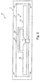
- Fig. 4 is a plan view of an RFID tag as an embodiment of the present invention. Covers such as a cover sheet are removed in this Fig. 4, too.
- the RFID tag 10 shown in this Fig. 4 includes an antenna pattern 12 as a dipole antenna made up of mono pole patterns 121, 122 formed on a base sheet 11 and an IC chip 13 connected by means of flip chip (see Fig. 2) at ends of the two mono pole patterns 121, 122. Furthermore, this antenna pattern 12 includes a correction pattern 123 which bypasses the IC chip 13 and connects the mono pole patterns 121, 122.
- This correction pattern 123 is a pattern which operates as an inductor L to cancel out the parasitic capacitance C explained with reference to Fig. 2.
- the RFID tag 10 shown in Fig. 4 includes a loop peeling detection pattern 16 made of a relatively brittle conductive material such as silver paste in an area enclosed by the two mono pole patterns 121, 122 and correction pattern 123 on the base sheet 11.
- a loop peeling detection pattern 16 made of a relatively brittle conductive material such as silver paste in an area enclosed by the two mono pole patterns 121, 122 and correction pattern 123 on the base sheet 11.
- Both ends of the loop of this peeling detection pattern 16 is also connected to the IC chip 13 by means of flip chip having the same structure (see Fig. 2) as the connection structure with the antenna pattern 12 and this IC chip 13 includes not only a function of radio communication with an external device using the antenna pattern 12 but also a function of detecting the destruction of the peeling detection pattern 16.
- This peeling detection pattern 16 is provided with peeling detection points 161 at several locations on the loop.
- the antenna pattern 12, IC chip 13 and peeling detection pattern 16 are covered with a cover sheet.
- the peeling detection points 161 of the peeling detection pattern 16 are strongly bonded to the cover sheet, whereas parts other than the peeling detection points 161 of the peeling detection pattern 16 are bonded more strongly to the base sheet 11 than to the cover sheet. For this reason, when an attempt is made to peel off the cover sheet, the cover sheet is peeled off with only the peeling detection points 161 of the peeling detection pattern 16 remaining bonded to the cover sheet, the peeling detection pattern 16 is thereby destroyed and the IC chip 13 detects the destruction of the peeling detection pattern 16, thus preventing the tampering of this RFID tag 10.
- the peeling detection pattern 16 shown in Fig. 4 is formed within the area enclosed by the conductive pattern made up of the two mono pole patterns 121, 122 and correction pattern 123, and therefore it is possible to have little effect on the antenna characteristic such as the outreach of a radio communication using the antenna pattern 12 and there is no need to increase outside dimensions for providing this peeling detection pattern 16, either.
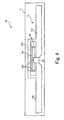
- Fig. 5 to Fig. 7 are enlarged views of the parts of the peeling detection pattern of the RFID tag according to this embodiment.
- Fig. 5 shows a state immediately after manufacturing
- Fig. 6 shows a state in which the tag is pasted to an object
- Fig. 7 shows a RFID tag peeled off the object.
- the RFID tag 10 shown in Fig. 5 is the RFID tag 10 explained with reference to Fig. 4 which is constructed of the base sheet 11, the antenna pattern 12 formed on the base sheet 11, the peeling detection pattern 16 (not shown in Fig. 5 to Fig. 7), the IC chip 13 connected to the antenna pattern 12 and peeling detection pattern 16 by means of flip chip.
- Fig. 5 to Fig. 7 the illustration of the connection structure between the peeling detection pattern 16 and IC chip 13 is omitted.
- the base sheet 11 is bonded to a mount 20 through an adhesive 31 and the base sheet 11, antenna pattern 12, peeling detection pattern 16 (not shown) and IC chip 13 are covered with a cover layer 32 made of opaque ink and further covered with a cover sheet 17.
- the cover sheet 17 and cover layer 32 have a structure similar to a so-called counterfeit prevention label.
- the cover layer 32 is constructed in such a way as to be easily separable, when the cover sheet 17 is peeled off, into peeling sections 32a which are peeled together with the cover sheet 17 while remaining bonded to the cover sheet 17 and remaining sections 32b which separate from the cover sheet 17 remaining on the base sheet 11 or pasting target 40 (see Fig. 6) side.
- an adhesive 33 having a strong adhesive force is also embedded in the part corresponding to the peeling detection points 161 of the peeling detection pattern 16 of the cover layer 32 and the peeling detection points 161 of the peeling detection pattern 16 is strongly bonded to the cover sheet 17 by this adhesive 33.
- the mount 20 shown in Fig. 5 is of a material having a low level of adhesion with the adhesive 31 and cover layer 32 on the back of the base sheet 11 and easily detachable and when this RFID tag is actually used, this RFID tag 10 is peeled off the mount 20 and actually used by being pasted to the pasting target 40 such as cardboard and plastics as shown in Fig. 6.
- the adhesive 31 on the back of the base sheet 11 and the remaining sections 32b of the cover layer 32 arranged in a mosaic shape have a predetermined adhesive force with respect to the pasting target 40, and after this RFID tag 10 is pasted to the pasting target 40, if the RFID tag 10 is peeled off the pasting target 40, the peeling sections 32a and the remaining sections 32b of the cover layer 32 are separated by a force much weaker than that of the adhesive 31 which pastes the base sheet 11 to the pasting target 40 as shown in Fig. 7.
- the peeling detection points 161 of the peeling detection pattern 16 is strongly bonded to the cover sheet 17 by the strong adhesive 33, and therefore the peeling detection points 161 are peeled from the peeling detection pattern 16 while remaining bonded to the cover sheet 17, which destroys the peeling detection pattern 16 and makes the peeling detection pattern 16 non-conducting and the IC chip 13 detects the fact that the peeling detection pattern 16 has become non-conducting and executes processing which has been incorporated beforehand against illegal peeling.
- the cover layer 32 is peeled in a patchy pattern, the peeling can be confirmed from appearances at first sight.
- Fig. 8 is a plan view of an RFID tag according to a second embodiment of the present invention.
- the RFID tag is shown with the cover sheet, etc., removed here, too.
- An antenna pattern 12 of the RFID tag 10 shown in this Fig. 8 is a conductive pattern of a loop antenna formed on a base sheet 11, both ends of which are connected to an IC chip 13 by means of flip chip (see Fig. 2).
- the antenna pattern 12 making up this loop antenna includes two extending sections 12a, 12b which extend from the IC chip 13, each end of which is connected to the IC chip 13, and a correction pattern 123 which bypasses the IC chip 13 and connects the two extending sections 12a, 12b.
- the correction pattern 123 includes double patterns of a pattern 123a and pattern 123b.
- a loop peeling detection pattern 16 made of silver paste, etc. is formed in an area enclosed by the two extending sections 12a, 12b of the antenna pattern 12 and the correction pattern 123 on the base sheet 11.
- the IC chip 13 incorporates a circuit which carries out a radio communication using the antenna pattern 12 of the loop antenna and detects a change of the peeling detection pattern 16 from a conductive state to non-conductive state (peeling detection).
- Fig. 9 is an enlarged view of the inside of the circle R in Fig. 8.
- the ends of the antenna pattern 12 connected to the IC chip 13 are formed into a small width. This is intended to reduce the parasitic capacitance C produced in that part as much as possible.
- the peeling detection pattern 16 is provided with peeling detection points 161 at several locations on the loop. These peeling detection points are strongly bonded to the cover sheet (not shown) as explained with reference to Fig. 5 to Fig. 7 and when this cover sheet is peeled, the peeling detection points 161 are peeled while remaining bonded to the cover sheet, which destroys the peeling detection pattern 16 and makes the peeling detection pattern 16 non-conducting and the IC chip 13 detects the peeling.
- this peeling detection pattern 16 is formed within the area enclosed by the two extending sections 12a, 12b of the antenna pattern 12 and the correction pattern 123, it is possible to detect the peeling reliably without deteriorating the characteristic as the antenna of the antenna pattern 12.
- the present invention is applicable regardless of the shape of the antenna pattern.
Landscapes
- Engineering & Computer Science (AREA)
- Computer Hardware Design (AREA)
- Microelectronics & Electronic Packaging (AREA)
- Physics & Mathematics (AREA)
- General Physics & Mathematics (AREA)
- Theoretical Computer Science (AREA)
- Computer Security & Cryptography (AREA)
- General Engineering & Computer Science (AREA)
- Details Of Aerials (AREA)
- Credit Cards Or The Like (AREA)
Applications Claiming Priority (1)
| Application Number | Priority Date | Filing Date | Title |
|---|---|---|---|
| JP2005108675A JP4750450B2 (ja) | 2005-04-05 | 2005-04-05 | Rfidタグ |
Publications (2)
| Publication Number | Publication Date |
|---|---|
| EP1710734A2 true EP1710734A2 (fr) | 2006-10-11 |
| EP1710734A3 EP1710734A3 (fr) | 2011-06-29 |
Family
ID=36582002
Family Applications (1)
| Application Number | Title | Priority Date | Filing Date |
|---|---|---|---|
| EP05255481A Withdrawn EP1710734A3 (fr) | 2005-04-05 | 2005-09-07 | Etiquette RFID |
Country Status (6)
| Country | Link |
|---|---|
| US (1) | US7277017B2 (fr) |
| EP (1) | EP1710734A3 (fr) |
| JP (1) | JP4750450B2 (fr) |
| KR (1) | KR100686573B1 (fr) |
| CN (1) | CN100474335C (fr) |
| TW (1) | TWI301947B (fr) |
Cited By (4)
| Publication number | Priority date | Publication date | Assignee | Title |
|---|---|---|---|---|
| DE102008059453A1 (de) * | 2008-10-20 | 2010-04-22 | Smartrac Ip B.V. | Transpondereinrichtung |
| EP2212969A4 (fr) * | 2007-10-11 | 2010-12-29 | 3M Innovative Properties Co | Étiquette rfid à antenne dipolaire modifiée |
| WO2011048234A1 (fr) * | 2009-10-07 | 2011-04-28 | Alfos Solutions, S.L. | Système de contrôle de produits sanitaires |
| US8289163B2 (en) | 2007-09-27 | 2012-10-16 | 3M Innovative Properties Company | Signal line structure for a radio-frequency identification system |
Families Citing this family (117)
| Publication number | Priority date | Publication date | Assignee | Title |
|---|---|---|---|---|
| JP4453582B2 (ja) * | 2005-03-16 | 2010-04-21 | 富士通株式会社 | Rfidタグ |
| US7519328B2 (en) | 2006-01-19 | 2009-04-14 | Murata Manufacturing Co., Ltd. | Wireless IC device and component for wireless IC device |
| US7557715B1 (en) * | 2006-02-08 | 2009-07-07 | Tc License Ltd. | Destructible RFID transponder |
| US20070205900A1 (en) * | 2006-03-03 | 2007-09-06 | Ipico Innovation Inc. | Rfid tag with antenna and sense conductor |
| CN102780085A (zh) | 2006-04-14 | 2012-11-14 | 株式会社村田制作所 | 天线 |
| US9064198B2 (en) | 2006-04-26 | 2015-06-23 | Murata Manufacturing Co., Ltd. | Electromagnetic-coupling-module-attached article |
| JP4208254B2 (ja) * | 2006-05-31 | 2009-01-14 | サンコール株式会社 | アンテナユニット,無線通信構造体及びアンテナ構造 |
| JP4281850B2 (ja) | 2006-06-30 | 2009-06-17 | 株式会社村田製作所 | 光ディスク |
| US20080055045A1 (en) * | 2006-08-31 | 2008-03-06 | 3M Innovative Properties Company | Rfid tag including a three-dimensional antenna |
| DE112007002024B4 (de) | 2006-09-26 | 2010-06-10 | Murata Mfg. Co., Ltd., Nagaokakyo-shi | Induktiv gekoppeltes Modul und Element mit induktiv gekoppeltem Modul |
| KR100842320B1 (ko) | 2006-11-06 | 2008-06-30 | 아시아나아이디티 주식회사 | 금속 부착형 태그 안테나 |
| JP2008123083A (ja) * | 2006-11-09 | 2008-05-29 | Dainippon Printing Co Ltd | 非接触icタグラベルと航空手荷物タグラベル、および非接触icタグラベルの製造方法 |
| KR100841646B1 (ko) * | 2006-11-17 | 2008-06-27 | 엘에스산전 주식회사 | 무선 주파수 식별 태그 안테나 |
| CN101000659B (zh) * | 2006-12-26 | 2010-08-11 | 上海复旦天臣新技术有限公司 | 具有防伪及防转移功能的非接触式电子标签及其制备方法 |
| JP5029026B2 (ja) * | 2007-01-18 | 2012-09-19 | 富士通株式会社 | 電子装置の製造方法 |
| WO2008096576A1 (fr) | 2007-02-06 | 2008-08-14 | Murata Manufacturing Co., Ltd. | Matériau d'emballage pourvu d'un module couplé de façon électromagnétique |
| JP4837597B2 (ja) * | 2007-02-19 | 2011-12-14 | トッパン・フォームズ株式会社 | 非接触型データ受送信体 |
| KR101294579B1 (ko) * | 2007-04-02 | 2013-08-07 | 엘지이노텍 주식회사 | 안테나 |
| JP5024372B2 (ja) | 2007-04-06 | 2012-09-12 | 株式会社村田製作所 | 無線icデバイス |
| WO2008126649A1 (fr) | 2007-04-09 | 2008-10-23 | Murata Manufacturing Co., Ltd. | Dispositif sans fil à circuit intégré |
| US8235299B2 (en) | 2007-07-04 | 2012-08-07 | Murata Manufacturing Co., Ltd. | Wireless IC device and component for wireless IC device |
| WO2008136226A1 (fr) | 2007-04-26 | 2008-11-13 | Murata Manufacturing Co., Ltd. | Dispositif à circuit intégré sans fil |
| WO2008136220A1 (fr) | 2007-04-27 | 2008-11-13 | Murata Manufacturing Co., Ltd. | Dispositif sans fil à circuit intégré |
| JP4433097B2 (ja) | 2007-04-27 | 2010-03-17 | 株式会社村田製作所 | 無線icデバイス |
| JP5054423B2 (ja) * | 2007-05-01 | 2012-10-24 | トッパン・フォームズ株式会社 | Rfidメディア |
| JP2008282103A (ja) * | 2007-05-08 | 2008-11-20 | Yoshikawa Rf System Kk | データキャリア及びリーダ/ライタ装置 |
| JP4666102B2 (ja) | 2007-05-11 | 2011-04-06 | 株式会社村田製作所 | 無線icデバイス |
| WO2009008296A1 (fr) | 2007-07-09 | 2009-01-15 | Murata Manufacturing Co., Ltd. | Dispositif à circuit intégré sans fil |
| CN104540317B (zh) | 2007-07-17 | 2018-11-02 | 株式会社村田制作所 | 印制布线基板 |
| US20090021352A1 (en) | 2007-07-18 | 2009-01-22 | Murata Manufacturing Co., Ltd. | Radio frequency ic device and electronic apparatus |
| JP5104865B2 (ja) | 2007-07-18 | 2012-12-19 | 株式会社村田製作所 | 無線icデバイス |
| JP4434311B2 (ja) | 2007-07-18 | 2010-03-17 | 株式会社村田製作所 | 無線icデバイスおよびその製造方法 |
| US20090085750A1 (en) * | 2007-09-27 | 2009-04-02 | 3M Innovative Properties Company | Extended RFID tag |
| CN101595599B (zh) | 2007-12-20 | 2013-05-01 | 株式会社村田制作所 | 无线ic器件 |
| EP2557528A3 (fr) | 2007-12-26 | 2017-01-18 | Murata Manufacturing Co., Ltd. | Dispositif d'antenne et dispositif à circuit intégré sans fil |
| EP2251934B1 (fr) | 2008-03-03 | 2018-05-02 | Murata Manufacturing Co. Ltd. | Dispositif à ci sans fil et système de communication sans fil |
| JP4518211B2 (ja) | 2008-03-03 | 2010-08-04 | 株式会社村田製作所 | 複合アンテナ |
| JP4404166B2 (ja) | 2008-03-26 | 2010-01-27 | 株式会社村田製作所 | 無線icデバイス |
| JP4535209B2 (ja) | 2008-04-14 | 2010-09-01 | 株式会社村田製作所 | 無線icデバイス、電子機器及び無線icデバイスの共振周波数の調整方法 |
| KR20110002837A (ko) * | 2008-04-24 | 2011-01-10 | 도레이 카부시키가이샤 | 비접촉 ic 태그 |
| CN103295056B (zh) | 2008-05-21 | 2016-12-28 | 株式会社村田制作所 | 无线ic器件 |
| WO2009142068A1 (fr) | 2008-05-22 | 2009-11-26 | 株式会社村田製作所 | Dispositif à circuit intégré sans fil et son procédé de fabrication |
| CN104077622B (zh) | 2008-05-26 | 2016-07-06 | 株式会社村田制作所 | 无线ic器件系统及无线ic器件的真伪判定方法 |
| EP2282372B1 (fr) | 2008-05-28 | 2019-09-11 | Murata Manufacturing Co. Ltd. | Dispositif à circuit intégré sans fil et composant pour dispositif à circuit intégré sans fil |
| JP4557186B2 (ja) | 2008-06-25 | 2010-10-06 | 株式会社村田製作所 | 無線icデバイスとその製造方法 |
| EP2306586B1 (fr) | 2008-07-04 | 2014-04-02 | Murata Manufacturing Co. Ltd. | Dispositif à circuit intégré sans fil |
| US8319610B2 (en) * | 2008-08-12 | 2012-11-27 | Industrial Technology Research Institute | Radio-frequency identification (RFID) antenna, tags and communications systems using the same |
| WO2010021217A1 (fr) | 2008-08-19 | 2010-02-25 | 株式会社村田製作所 | Dispositif à circuit intégré sans fil et procédé de fabrication de celui-ci |
| US20100096455A1 (en) * | 2008-10-16 | 2010-04-22 | Merrick Systems Inc. | Edge mounted rfid tag |
| WO2010047214A1 (fr) | 2008-10-24 | 2010-04-29 | 株式会社村田製作所 | Dispositif ci radio |
| TWI385854B (zh) * | 2008-10-24 | 2013-02-11 | Cheng Uei Prec Ind Co Ltd | 射頻識別天線和具有該射頻識別天線的電子產品 |
| DE112009002399B4 (de) | 2008-10-29 | 2022-08-18 | Murata Manufacturing Co., Ltd. | Funk-IC-Bauelement |
| DE112009002384B4 (de) | 2008-11-17 | 2021-05-06 | Murata Manufacturing Co., Ltd. | Antenne und Drahtlose-IC-Bauelement |
| KR101030372B1 (ko) * | 2008-12-18 | 2011-04-20 | 아주대학교산학협력단 | 광대역에서 일정한 준 등방성 특성을 가지는 유-형태의 알에프아이디 태그 안테나 |
| CN102273012B (zh) | 2009-01-09 | 2013-11-20 | 株式会社村田制作所 | 无线ic器件及无线ic模块 |
| JP5041077B2 (ja) | 2009-01-16 | 2012-10-03 | 株式会社村田製作所 | 高周波デバイス及び無線icデバイス |
| EP2385580B1 (fr) | 2009-01-30 | 2014-04-09 | Murata Manufacturing Co., Ltd. | Antenne et dispositif de circuit intégré sans fil |
| JP5172752B2 (ja) * | 2009-03-23 | 2013-03-27 | 株式会社日立製作所 | Rfタグリーダ回路 |
| JP5510450B2 (ja) | 2009-04-14 | 2014-06-04 | 株式会社村田製作所 | 無線icデバイス |
| EP2424041B1 (fr) | 2009-04-21 | 2018-11-21 | Murata Manufacturing Co., Ltd. | Appareil d'antenne et procédé de réglage de la fréquence de résonance de celui-ci |
| WO2010140429A1 (fr) | 2009-06-03 | 2010-12-09 | 株式会社村田製作所 | Dispositif de circuit intégré sans fil et son procédé de production |
| KR101139317B1 (ko) | 2009-06-16 | 2012-04-26 | 건국대학교 산학협력단 | 알에프아이디 태그 안테나 |
| JP5516580B2 (ja) | 2009-06-19 | 2014-06-11 | 株式会社村田製作所 | 無線icデバイス及び給電回路と放射板との結合方法 |
| JP5182431B2 (ja) | 2009-09-28 | 2013-04-17 | 株式会社村田製作所 | 無線icデバイスおよびそれを用いた環境状態検出方法 |
| CN102577646B (zh) | 2009-09-30 | 2015-03-04 | 株式会社村田制作所 | 电路基板及其制造方法 |
| JP5304580B2 (ja) | 2009-10-02 | 2013-10-02 | 株式会社村田製作所 | 無線icデバイス |
| CN102576939B (zh) | 2009-10-16 | 2015-11-25 | 株式会社村田制作所 | 天线及无线ic器件 |
| JP5418600B2 (ja) | 2009-10-27 | 2014-02-19 | 株式会社村田製作所 | 送受信装置及び無線タグ読み取り装置 |
| WO2011055702A1 (fr) | 2009-11-04 | 2011-05-12 | 株式会社村田製作所 | Étiquette à circuit radio intégré, lecteur/enregistreur, et système de traitement d'information |
| CN102576930A (zh) | 2009-11-04 | 2012-07-11 | 株式会社村田制作所 | 通信终端及信息处理系统 |
| JP5327334B2 (ja) | 2009-11-04 | 2013-10-30 | 株式会社村田製作所 | 通信端末及び情報処理システム |
| GB2487491B (en) | 2009-11-20 | 2014-09-03 | Murata Manufacturing Co | Antenna device and mobile communication terminal |
| JP4978756B2 (ja) | 2009-12-24 | 2012-07-18 | 株式会社村田製作所 | 通信端末 |
| WO2011108341A1 (fr) | 2010-03-03 | 2011-09-09 | 株式会社村田製作所 | Dispositif de radiocommunication et terminal de radiocommunication |
| JP5652470B2 (ja) | 2010-03-03 | 2015-01-14 | 株式会社村田製作所 | 無線通信モジュール及び無線通信デバイス |
| CN102576940B (zh) | 2010-03-12 | 2016-05-04 | 株式会社村田制作所 | 无线通信器件及金属制物品 |
| CN102194142A (zh) * | 2010-03-18 | 2011-09-21 | 优仕达资讯股份有限公司 | 射频识别标签 |
| CN102668241B (zh) | 2010-03-24 | 2015-01-28 | 株式会社村田制作所 | Rfid系统 |
| JP5630499B2 (ja) | 2010-03-31 | 2014-11-26 | 株式会社村田製作所 | アンテナ装置及び無線通信デバイス |
| JP5299351B2 (ja) | 2010-05-14 | 2013-09-25 | 株式会社村田製作所 | 無線icデバイス |
| JP5170156B2 (ja) | 2010-05-14 | 2013-03-27 | 株式会社村田製作所 | 無線icデバイス |
| JP5376060B2 (ja) | 2010-07-08 | 2013-12-25 | 株式会社村田製作所 | アンテナ及びrfidデバイス |
| GB2495418B (en) | 2010-07-28 | 2017-05-24 | Murata Manufacturing Co | Antenna apparatus and communication terminal instrument |
| WO2012020748A1 (fr) | 2010-08-10 | 2012-02-16 | 株式会社村田製作所 | Carte de circuit imprimé et système de communication sans fil |
| JP5234071B2 (ja) | 2010-09-03 | 2013-07-10 | 株式会社村田製作所 | Rficモジュール |
| CN103038939B (zh) | 2010-09-30 | 2015-11-25 | 株式会社村田制作所 | 无线ic器件 |
| CN105226382B (zh) | 2010-10-12 | 2019-06-11 | 株式会社村田制作所 | 天线装置及终端装置 |
| GB2501385B (en) | 2010-10-21 | 2015-05-27 | Murata Manufacturing Co | Communication terminal device |
| CN105048058B (zh) | 2011-01-05 | 2017-10-27 | 株式会社村田制作所 | 无线通信器件 |
| JP5304956B2 (ja) | 2011-01-14 | 2013-10-02 | 株式会社村田製作所 | Rfidチップパッケージ及びrfidタグ |
| CN104899639B (zh) | 2011-02-28 | 2018-08-07 | 株式会社村田制作所 | 无线通信器件 |
| JP5630566B2 (ja) | 2011-03-08 | 2014-11-26 | 株式会社村田製作所 | アンテナ装置及び通信端末機器 |
| JP5273326B2 (ja) | 2011-04-05 | 2013-08-28 | 株式会社村田製作所 | 無線通信デバイス |
| WO2012141070A1 (fr) | 2011-04-13 | 2012-10-18 | 株式会社村田製作所 | Dispositif à circuit intégré sans fil et terminal de communication sans fil |
| WO2012157596A1 (fr) | 2011-05-16 | 2012-11-22 | 株式会社村田製作所 | Dispositif à ic sans fil |
| WO2013008874A1 (fr) | 2011-07-14 | 2013-01-17 | 株式会社村田製作所 | Dispositif de communication sans fil |
| JP5333707B2 (ja) | 2011-07-15 | 2013-11-06 | 株式会社村田製作所 | 無線通信デバイス |
| WO2013011865A1 (fr) | 2011-07-19 | 2013-01-24 | 株式会社村田製作所 | Module d'antenne, dispositif d'antenne, étiquette rfid et dispositif terminal de communication |
| JP5418737B2 (ja) | 2011-09-09 | 2014-02-19 | 株式会社村田製作所 | アンテナ装置および無線デバイス |
| US9076095B2 (en) * | 2011-12-01 | 2015-07-07 | Vallourec Oil And Gas France, S.A.S. | Extendable identification tag |
| CN103380432B (zh) | 2011-12-01 | 2016-10-19 | 株式会社村田制作所 | 无线ic器件及其制造方法 |
| JP5354137B1 (ja) | 2012-01-30 | 2013-11-27 | 株式会社村田製作所 | 無線icデバイス |
| WO2013125610A1 (fr) | 2012-02-24 | 2013-08-29 | 株式会社村田製作所 | Dispositif d'antenne et dispositif de communication sans fil |
| WO2013153697A1 (fr) | 2012-04-13 | 2013-10-17 | 株式会社村田製作所 | Procédé d'inspection d'étiquette d'identification par radiofréquence (rfid) et dispositif d'inspection |
| TWI506857B (zh) * | 2012-12-14 | 2015-11-01 | Arcadyan Technology Corp | 應用於射頻檢測程序之印刷式天線模組 |
| CN105408918B (zh) * | 2013-07-31 | 2018-07-10 | 富士通株式会社 | Rfid标签、以及rfid系统 |
| JP6079520B2 (ja) * | 2013-09-12 | 2017-02-15 | 凸版印刷株式会社 | 非接触icラベル |
| US9390367B2 (en) | 2014-07-08 | 2016-07-12 | Wernher von Braun Centro de Pesquisas Avancadas | RFID tag and RFID tag antenna |
| CN104527246B (zh) * | 2014-12-23 | 2017-02-01 | 睿芯(大连)股份有限公司 | 一种含有rfid电子标签的彩色包装产品的凹版印刷方法 |
| US9966925B2 (en) * | 2016-01-28 | 2018-05-08 | Analog Devices, Inc. | Apparatus and method to balance the parasitic capacitances between metal tracks on an integrated circuit chip |
| TWI626790B (zh) * | 2016-08-18 | 2018-06-11 | 創新聯合科技股份有限公司 | Long-distance radio frequency electronic identification tire structure |
| TWI628852B (zh) * | 2016-09-07 | 2018-07-01 | 中國鋼鐵股份有限公司 | Radio frequency identification tag and label paper product using the same |
| WO2018045550A1 (fr) * | 2016-09-09 | 2018-03-15 | Hong Kong R&D Centre for Logistics and Supply Chain Management Enabling Technologies Limited | Dispositif de communication radiofréquence et son procédé d'utilisation |
| TWI624995B (zh) * | 2016-09-09 | 2018-05-21 | 創新聯合科技股份有限公司 | Long-range radio frequency anti-metal identification tag |
| US11544697B2 (en) * | 2017-06-12 | 2023-01-03 | The Coca-Cola Company | Low cost control pour |
| JP7587979B2 (ja) * | 2020-12-17 | 2024-11-21 | 大王製紙株式会社 | Rfidタグ及びその製造方法 |
| US12393946B2 (en) * | 2021-12-27 | 2025-08-19 | Mastercard International Incorporated | System and method for authentication and payment while wearing a face covering |
Citations (3)
| Publication number | Priority date | Publication date | Assignee | Title |
|---|---|---|---|---|
| US6421013B1 (en) | 1999-10-04 | 2002-07-16 | Amerasia International Technology, Inc. | Tamper-resistant wireless article including an antenna |
| US20030075608A1 (en) | 2000-03-21 | 2003-04-24 | Atherton Peter S | Tamper indicating radio frequency identification label |
| JP2003524811A (ja) | 1998-10-15 | 2003-08-19 | アメラシア インターナショナル テクノロジー,インコーポレイテッド | 埋込み電子装置を有する製品とその製作方法 |
Family Cites Families (3)
| Publication number | Priority date | Publication date | Assignee | Title |
|---|---|---|---|---|
| JP3911900B2 (ja) * | 1999-04-05 | 2007-05-09 | 株式会社日立製作所 | Icシール |
| US6894624B2 (en) * | 2000-07-04 | 2005-05-17 | Credipass Co., Ltd. | Passive transponder identification and credit-card type transponder |
| US7336243B2 (en) * | 2003-05-29 | 2008-02-26 | Sky Cross, Inc. | Radio frequency identification tag |
-
2005
- 2005-04-05 JP JP2005108675A patent/JP4750450B2/ja not_active Expired - Fee Related
- 2005-09-07 EP EP05255481A patent/EP1710734A3/fr not_active Withdrawn
- 2005-09-09 TW TW094131119A patent/TWI301947B/zh not_active IP Right Cessation
- 2005-09-22 US US11/232,035 patent/US7277017B2/en not_active Expired - Fee Related
- 2005-09-29 CN CNB2005101076831A patent/CN100474335C/zh not_active Expired - Fee Related
- 2005-09-30 KR KR1020050092537A patent/KR100686573B1/ko not_active Expired - Fee Related
Patent Citations (3)
| Publication number | Priority date | Publication date | Assignee | Title |
|---|---|---|---|---|
| JP2003524811A (ja) | 1998-10-15 | 2003-08-19 | アメラシア インターナショナル テクノロジー,インコーポレイテッド | 埋込み電子装置を有する製品とその製作方法 |
| US6421013B1 (en) | 1999-10-04 | 2002-07-16 | Amerasia International Technology, Inc. | Tamper-resistant wireless article including an antenna |
| US20030075608A1 (en) | 2000-03-21 | 2003-04-24 | Atherton Peter S | Tamper indicating radio frequency identification label |
Cited By (5)
| Publication number | Priority date | Publication date | Assignee | Title |
|---|---|---|---|---|
| US8289163B2 (en) | 2007-09-27 | 2012-10-16 | 3M Innovative Properties Company | Signal line structure for a radio-frequency identification system |
| EP2212969A4 (fr) * | 2007-10-11 | 2010-12-29 | 3M Innovative Properties Co | Étiquette rfid à antenne dipolaire modifiée |
| US8717244B2 (en) | 2007-10-11 | 2014-05-06 | 3M Innovative Properties Company | RFID tag with a modified dipole antenna |
| DE102008059453A1 (de) * | 2008-10-20 | 2010-04-22 | Smartrac Ip B.V. | Transpondereinrichtung |
| WO2011048234A1 (fr) * | 2009-10-07 | 2011-04-28 | Alfos Solutions, S.L. | Système de contrôle de produits sanitaires |
Also Published As
| Publication number | Publication date |
|---|---|
| KR100686573B1 (ko) | 2007-02-26 |
| KR20060106597A (ko) | 2006-10-12 |
| JP4750450B2 (ja) | 2011-08-17 |
| TWI301947B (en) | 2008-10-11 |
| CN100474335C (zh) | 2009-04-01 |
| US7277017B2 (en) | 2007-10-02 |
| CN1848143A (zh) | 2006-10-18 |
| JP2006285911A (ja) | 2006-10-19 |
| US20060220871A1 (en) | 2006-10-05 |
| EP1710734A3 (fr) | 2011-06-29 |
| TW200636594A (en) | 2006-10-16 |
Similar Documents
| Publication | Publication Date | Title |
|---|---|---|
| US7277017B2 (en) | RFID tag | |
| EP2097856B1 (fr) | Etiquette d'identification par radio-frequence a fenetre a revetement anti-adhesif et procede de fabrication associe | |
| US6549176B2 (en) | RFID tag having integral electrical bridge and method of assembling the same | |
| US7274297B2 (en) | RFID tag and method of manufacture | |
| EP3564860B1 (fr) | Antenne à étiquette rfid montable souple en forme de l | |
| EP1703447B1 (fr) | Etiquette de type RFID | |
| AU2016203242A1 (en) | A modular radio frequency identification tagging method | |
| KR20080042660A (ko) | Rfic 태그와 그 사용 방법 | |
| JP2007534196A (ja) | 平坦な台から成る3次元アンテナアレイを有するセキュリティタグとその製作方法 | |
| KR20190143471A (ko) | 전기 및/또는 전자 모듈을 포함하는 조정가능한 lc 회로를 갖는 무선주파수 디바이스 | |
| EP3528176B1 (fr) | Anneau intelligent sans contact | |
| US7427919B2 (en) | RFID tag set, RFID tag and RFID tag component | |
| JP2008186353A (ja) | Icタグ用アンテナ | |
| KR200434465Y1 (ko) | 알에프아이디 태그 | |
| US20180351233A1 (en) | Single-face antenna module comprising cms device | |
| KR100797555B1 (ko) | 전파 식별 시스템용 트랜스폰더 | |
| KR100883829B1 (ko) | 알에프아이디 안테나의 제조방법 | |
| KR101914422B1 (ko) | Ic칩 동조 기능을 가지는 ic 카드 및 이의 신호 송수신 방법 | |
| KR100735618B1 (ko) | 알에프아이디 안테나 및 그 제조방법 | |
| KR100883830B1 (ko) | 알에프아이디 안테나의 제조방법 | |
| WO2008115022A1 (fr) | Antenne d'identification par radiofréquence et son procédé de fabrication | |
| KR20050120481A (ko) | 전자 무선 인식 장치 및 전자 무선 인식 장치의 제조방법 | |
| EP4327243A1 (fr) | Dispositif rfid extensible et modulaire |
Legal Events
| Date | Code | Title | Description |
|---|---|---|---|
| PUAI | Public reference made under article 153(3) epc to a published international application that has entered the european phase |
Free format text: ORIGINAL CODE: 0009012 |
|
| AK | Designated contracting states |
Kind code of ref document: A2 Designated state(s): AT BE BG CH CY CZ DE DK EE ES FI FR GB GR HU IE IS IT LI LT LU LV MC NL PL PT RO SE SI SK TR |
|
| AX | Request for extension of the european patent |
Extension state: AL BA HR MK YU |
|
| PUAL | Search report despatched |
Free format text: ORIGINAL CODE: 0009013 |
|
| AK | Designated contracting states |
Kind code of ref document: A3 Designated state(s): AT BE BG CH CY CZ DE DK EE ES FI FR GB GR HU IE IS IT LI LT LU LV MC NL PL PT RO SE SI SK TR |
|
| AX | Request for extension of the european patent |
Extension state: AL BA HR MK YU |
|
| AKY | No designation fees paid | ||
| REG | Reference to a national code |
Ref country code: DE Ref legal event code: R108 Effective date: 20120307 |
|
| STAA | Information on the status of an ep patent application or granted ep patent |
Free format text: STATUS: THE APPLICATION IS DEEMED TO BE WITHDRAWN |
|
| 18D | Application deemed to be withdrawn |
Effective date: 20111230 |