EP1715436A2 - Schutz des Ablaufs eines von einem integrierten Schaltkreis ausgeführten Programms oder von Daten, die in diesem Schaltkreis enthalten sind - Google Patents
Schutz des Ablaufs eines von einem integrierten Schaltkreis ausgeführten Programms oder von Daten, die in diesem Schaltkreis enthalten sind Download PDFInfo
- Publication number
- EP1715436A2 EP1715436A2 EP06112843A EP06112843A EP1715436A2 EP 1715436 A2 EP1715436 A2 EP 1715436A2 EP 06112843 A EP06112843 A EP 06112843A EP 06112843 A EP06112843 A EP 06112843A EP 1715436 A2 EP1715436 A2 EP 1715436A2
- Authority
- EP
- European Patent Office
- Prior art keywords
- integrated circuit
- volatile memory
- circuit
- volatile
- memory
- Prior art date
- Legal status (The legal status is an assumption and is not a legal conclusion. Google has not performed a legal analysis and makes no representation as to the accuracy of the status listed.)
- Withdrawn
Links
Images

Classifications
-
- G—PHYSICS
- G06—COMPUTING OR CALCULATING; COUNTING
- G06F—ELECTRIC DIGITAL DATA PROCESSING
- G06F21/00—Security arrangements for protecting computers, components thereof, programs or data against unauthorised activity
- G06F21/70—Protecting specific internal or peripheral components, in which the protection of a component leads to protection of the entire computer
- G06F21/71—Protecting specific internal or peripheral components, in which the protection of a component leads to protection of the entire computer to assure secure computing or processing of information
- G06F21/75—Protecting specific internal or peripheral components, in which the protection of a component leads to protection of the entire computer to assure secure computing or processing of information by inhibiting the analysis of circuitry or operation
- G06F21/755—Protecting specific internal or peripheral components, in which the protection of a component leads to protection of the entire computer to assure secure computing or processing of information by inhibiting the analysis of circuitry or operation with measures against power attack
-
- G—PHYSICS
- G06—COMPUTING OR CALCULATING; COUNTING
- G06F—ELECTRIC DIGITAL DATA PROCESSING
- G06F21/00—Security arrangements for protecting computers, components thereof, programs or data against unauthorised activity
- G06F21/70—Protecting specific internal or peripheral components, in which the protection of a component leads to protection of the entire computer
- G06F21/71—Protecting specific internal or peripheral components, in which the protection of a component leads to protection of the entire computer to assure secure computing or processing of information
- G06F21/77—Protecting specific internal or peripheral components, in which the protection of a component leads to protection of the entire computer to assure secure computing or processing of information in smart cards
Definitions
- the present invention generally relates to electronic circuits, and more particularly, the protection of the progress of a program executed by an integrated circuit or of digital quantities contained in an integrated circuit against an extraction of these data, following a disturbance of the operation. of the circuit.
- the invention relates, for example, protection against data extraction following fault injections in the operation of the circuit and more particularly in a program using the digital quantity or quantities to be protected.
- the invention relates to protection against a disturbance in the course of a program following a fault injection.
- the present invention applies, for example, to smart cards.
- FIG. 1 very schematically shows in the form of blocks an example of a simplified architecture of an integrated circuit 1, for example a smart card, of the type to which the present invention applies.
- the circuit 1 comprises a central processing unit 11 (CPU) associated with several memories 12 (MEM) among which at least one random access memory of the RAM type and a rewritable non-volatile memory, for example of the EEPROM type, and an input / output (I / O) circuit 13 allowing the exchange of data with the Outside the circuit 1.
- the different elements communicate by one or more internal buses 14 of data, addresses and commands.
- a category of attacks that can be made by fraudsters to obtain confidential data of the chip 1 relates to the so-called attacks by injection of faults. These attacks consist in disrupting the operation of component 1, for example, by means of radiation (laser, infrared, X-rays, etc.) or by other means (for example by acting on the power supply of the component) . In the case of data piracy, these attacks are generally iterative to successively discover the different bits of a secret quantity. Injections of fault usually cause a diversion in the course of a program. Such a trap can also be searched by a hacker, regardless of a data output to, for example, skip a protection mechanism, identification, etc.
- SPA simple power analysis
- Some integrated circuits include software and / or hardware tools to detect disturbances in their operation by verifying that a program has executed correctly. For example, we execute twice the same instructions and we check that they lead to the same result, or a signature calculation is performed on data extracted from the memory.
- the circuit includes light temperature detectors, etc. to detect a possible disturbance.
- FIG. 2 is a partial and very schematic representation of a conventional example of a mechanism of an integrated circuit 1 for protecting confidential data contained therein.
- the circuit 1 comprises one or more hardware detectors 21 (H DETECT) of the type of voltage, temperature, light sensor, etc. and / or one or more software detectors 22 (S DETECT) of the signature calculation type, calculation of a correction code, etc.
- the results of the detector (s) 21 and 22 are interpreted by a circuit or a program for monitoring the operation of the circuit (block 23, TRACK).
- the mechanism 23 causes either the writing (WR) of a control word (EEFLAG) in nonvolatile memory 121 (EEPROM), or the erasure (CLR) of this memory, at least for this which concerns the part containing data or secret algorithms of the circuit 1.
- WR writing
- EFLAG nonvolatile memory 121
- CLR erasure
- FIG. 3 illustrates the operation of the detection mechanism represented in FIG. 2.
- EXEC execution of a program 31 (PROGRAM) by the central unit (11, FIG. 1) of the integrated circuit
- FULT fault injection
- FAULT detection mechanism
- DETECT DETECT
- TRACK monitoring mechanism
- This detection leads to the processing of an alarm (block 23 ', ALARM) which causes writing or erasure (block 25, WR / CLR) in the non-volatile memory.
- a disadvantage of this kind of mechanism is that the current signature of a programming in a non-volatile EEPROM type memory is very characteristic and easy to detect by monitoring the consumption of the integrated circuit 1. Therefore, a fraudster who in parallel performs an analysis (ANALYSIS) of the circuit consumption is able to detecting, following its fault injection, the reaction of the circuit by an attempt to write to the non-volatile memory. The fraudster can then cause an immediate stop of the supply of the circuit (block 35, I DET / PW STOP) and thus prevent the execution of the countermeasure (block 25). Power failure can take various forms (for example, abrupt card output from a reader in the case of a smart card with contacts or removal of the remote power carrier in the case of a contactless card).
- the fraudster is able to suppress the power supply of the integrated circuit to prevent writing into the non-volatile memory or its erasure, it can re-iterate its attack by injecting faults and, for example, finish to obtain the digital quantity or quantities that are supposed to remain secret.
- the present invention aims to overcome all or part of the disadvantages of the known protection mechanisms of an integrated circuit following fault injection detection.
- the present invention more specifically aims at preventing a fraudster from preventing the execution of a write mechanism in non-volatile memory following detection of attempted fraud.
- the invention also aims to propose a solution compatible with the hardware elements of conventional integrated circuits.
- the invention also aims to propose a solution that applies regardless of the purpose of the fault injection (data output or simple diversion of a program).
- the intervention in non-volatile memory consists of copying information representative of the value of the variable of the volatile storage element into an area of the non-volatile memory.
- the method serves to protect the progress of a program executed by the integrated circuit.
- the content of said non-volatile memory information is tested to decide on the erasure of at least a part of this non-volatile memory.
- the method serves to protect a digital quantity contained in said non-volatile memory.
- the content of said non-volatile memory information conditions the data output of the integrated circuit.
- the intervention on the non-volatile memory is an at least partial erasure of this memory.
- the intervention on the non-volatile memory is performed periodically.
- said volatile storage element is a register of a central processing unit of the integrated circuit.
- said volatile storage element is an area of a volatile memory of the integrated circuit.
- the present invention also provides an integrated circuit comprising at least one central processing unit, a first non-volatile memory and a second volatile memory, at least one detector of an attempt to disturb the operation of the circuit, and such a protection mechanism.
- the present invention also provides a smart card, including such an integrated circuit.
- a characteristic of an embodiment of the present invention is, in the event of detection of a fault injection (whether intentional or accidental), of updating a variable in a volatile storage element of the circuit. integrated, then treat this information to copy in a non-volatile memory or erasure of at least the confidential data it contains, in a decorated manner of the detection.
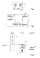
- FIG. 4 partially shows, in a very schematic and block form, an embodiment of an integrated circuit 1 provided with a protection mechanism according to the present invention.
- the circuit 1 comprises one or more hardware detectors 21 (H DETECT) of possible disturbances on the operation of the integrated circuit or the execution of a program, and / or one or more software detectors 22 (S DETECT).
- H DETECT hardware detectors 21
- S DETECT software detectors 22
- TRACK hardware and / or software mechanism 43
- the mechanism 43 in the event of detection of a fault originating, for example, from an attempted fraud, causes the writing (WR) of a variable (FLAG) in a zone of volatile memory 122 (SRAM) of the integrated circuit 1.
- the recording of such a variable is not detectable on the consumption of the circuit insofar as it does not differ from normal and frequent program accesses in this memory nonvolatile.
- the variable FLAG is stored in a register of the central unit.
- the content of the FLAG variable in volatile memory is exploited on a regular basis, preferably periodically by means of a time counter (block 45, TIMER) of the central unit, for intervention on a rewritable non-volatile memory 121 (EEPROM).
- TIMER time counter
- EEPROM rewritable non-volatile memory
- an EEFLAG word is written (WR) in a zone (address) of the non-volatile memory 121.
- WR write
- a zone address
- the non-volatile memory 121 For example, it is a copy of the contents of the variable FLAG of memory 122.
- the FLAG variable of the volatile memory indicates the detection of an attempted fraud
- at least the area of the rewritable non-volatile memory 121 containing confidential data is erased (CLR).
- FIG. 5 very schematically illustrates a mode of operation of the mechanism described with reference to FIG. 4.
- the mechanism of the invention positions the FLAG variable (block 53, WR FLAG) in volatile memory.
- the protection mechanism of the invention (PROTECT) writes periodically (blocks 55, WR EEFLAG) the content (more generally, information representative of this content) of the variable FLAG of the volatile memory in a non-volatile memory. volatile.
- the periodicity (T) between two writes in non-volatile memory is preferably set by a counter of the central unit (not shown in FIG. 5).
- the management of the input / output (I / O) data of the integrated circuit depends on a reading (READ EEFLAG) of the zone containing the information EEFLAG in non-volatile memory, followed by a test (TEST) of the value of this information before deciding the output (OUTPUT) of data to the outside of the circuit.
- the period T between two writes of the EEFLAG information is then chosen to be less than the execution time of the program between a sensitive zone liable to a fault injection and the call to the entry procedure. output, so that you can avoid data output.
- the reading of the EEFLAG word in the non-volatile memory takes place before any operation considered to be sensitive from the point of view of the security of the execution of a program or of confidential data contained in the document. integrated circuit and, preferably, after each start of a new program session. If the value corresponds to an identified attack, the CPU causes, for example, erasure of the sensitive data in the nonvolatile memory, or prevents the program from starting.
- the content of the FLAG variable is chosen to have a balanced current signature between the indicator states of a fault detection and indicator of normal operation (identical Hamming weight of the two values).
- the address of the EEFLAG indicator word is not always the same.
- An advantage of the present invention is that it makes undetectable to a potential fraudster the fact that a fault injection attack has been detected by the circuit.
- Another advantage of the invention is that it preserves the non-volatile treatment of this fraud detection.
- Another advantage of the present invention is that it is compatible with the different modes of operation of fraud detection detections whether it is a prohibition of data output of a smart card or a card. deleting a memory area thereof.
- Another advantage of the present invention is that it does not modify the detection of a fraud attempt in itself and is compatible with conventional disturbance detectors.
Landscapes
- Engineering & Computer Science (AREA)
- Physics & Mathematics (AREA)
- Computer Hardware Design (AREA)
- Theoretical Computer Science (AREA)
- Mathematical Physics (AREA)
- Computer Security & Cryptography (AREA)
- Software Systems (AREA)
- General Engineering & Computer Science (AREA)
- General Physics & Mathematics (AREA)
- Storage Device Security (AREA)
- Semiconductor Integrated Circuits (AREA)
Applications Claiming Priority (1)
| Application Number | Priority Date | Filing Date | Title |
|---|---|---|---|
| FR0551011 | 2005-04-21 |
Publications (2)
| Publication Number | Publication Date |
|---|---|
| EP1715436A2 true EP1715436A2 (de) | 2006-10-25 |
| EP1715436A3 EP1715436A3 (de) | 2007-03-28 |
Family
ID=34980022
Family Applications (1)
| Application Number | Title | Priority Date | Filing Date |
|---|---|---|---|
| EP06112843A Withdrawn EP1715436A3 (de) | 2005-04-21 | 2006-04-20 | Schutz des Ablaufs eines von einem integrierten Schaltkreis ausgeführten Programms oder von Daten, die in diesem Schaltkreis enthalten sind |
Country Status (2)
| Country | Link |
|---|---|
| US (1) | US7593258B2 (de) |
| EP (1) | EP1715436A3 (de) |
Families Citing this family (5)
| Publication number | Priority date | Publication date | Assignee | Title |
|---|---|---|---|---|
| FR2915007A1 (fr) * | 2007-04-12 | 2008-10-17 | St Microelectronics Sa | Protection de l'execution d'un programme |
| FR2924262B1 (fr) * | 2007-11-26 | 2009-12-11 | Sagem Securite | Procede de masquage de passage en fin de vie d'un dispositif electronique et dispositif comportant un module de controle correspondant |
| KR101269549B1 (ko) * | 2009-05-08 | 2013-06-04 | 한국전자통신연구원 | 오류 주입을 이용한 소프트웨어 신뢰성 테스트 시스템 및 방법 |
| US9122605B2 (en) * | 2013-09-23 | 2015-09-01 | Honeywell International Inc. | Methods for determining multiple simultaneous fault conditions |
| US12395502B2 (en) | 2022-09-28 | 2025-08-19 | Bank Of America Corporation | System and method for identifying and preventing misappropriation using normalized request sequences |
Citations (2)
| Publication number | Priority date | Publication date | Assignee | Title |
|---|---|---|---|---|
| US5465349A (en) * | 1990-10-19 | 1995-11-07 | Gemplus Card International | System for monitoring abnormal integrated circuit operating conditions and causing selective microprocessor interrupts |
| DE10303752A1 (de) | 2003-01-30 | 2004-08-19 | Infineon Technologies Ag | Steuerung einer Cachespeicheranordnung mit zufälligen Zurückschreibevorgängen |
Family Cites Families (8)
| Publication number | Priority date | Publication date | Assignee | Title |
|---|---|---|---|---|
| CA2350029A1 (en) * | 2001-06-08 | 2002-12-08 | Cloakware Corporation | Sustainable digital watermarking via tamper-resistant software |
| US6778066B2 (en) * | 2001-06-29 | 2004-08-17 | Hewlett-Packard Development Company, L.P. | Personal identification badge that resets on the removal of the badge from the wearer |
| AU2002344652A1 (en) | 2002-07-17 | 2004-02-02 | Etsuro Sakagami | Filtration method, filtration device, method of desalinating sea water by using the device, and method of desulfurizing petroleum |
| EP1383047A1 (de) * | 2002-07-18 | 2004-01-21 | Cp8 | Verfahren zur Sicherung der Ausführung eines Programms gegen Strahlungsangriffe oder ähnliches |
| FR2855286B1 (fr) * | 2003-05-22 | 2005-07-22 | Gemplus Card Int | Transmission securisee de donnees entre deux modules |
| FR2884000A1 (fr) * | 2005-04-05 | 2006-10-06 | St Microelectronics Sa | Coprocesseur securise comprenant des moyens pour empecher l'acces a un organe du coprocesseur |
| US7372304B2 (en) * | 2005-10-04 | 2008-05-13 | Stmicroelectronics, Inc. | System and method for glitch detection in a secure microcontroller |
| US7769165B2 (en) * | 2005-10-14 | 2010-08-03 | Microsoft Corporation | Semi-public white-box cipher |
-
2006
- 2006-04-20 EP EP06112843A patent/EP1715436A3/de not_active Withdrawn
- 2006-12-19 US US11/641,550 patent/US7593258B2/en not_active Expired - Lifetime
Patent Citations (2)
| Publication number | Priority date | Publication date | Assignee | Title |
|---|---|---|---|---|
| US5465349A (en) * | 1990-10-19 | 1995-11-07 | Gemplus Card International | System for monitoring abnormal integrated circuit operating conditions and causing selective microprocessor interrupts |
| DE10303752A1 (de) | 2003-01-30 | 2004-08-19 | Infineon Technologies Ag | Steuerung einer Cachespeicheranordnung mit zufälligen Zurückschreibevorgängen |
Non-Patent Citations (1)
| Title |
|---|
| HAGAI BAR-EL, THE SORCERER'S APPRENTICE GUIDE TO FAULT ATTACKS, 7 May 2004 (2004-05-07) |
Also Published As
| Publication number | Publication date |
|---|---|
| US7593258B2 (en) | 2009-09-22 |
| EP1715436A3 (de) | 2007-03-28 |
| US20070159882A1 (en) | 2007-07-12 |
Similar Documents
| Publication | Publication Date | Title |
|---|---|---|
| CA2053741C (fr) | Circuit integre a securite d'acces amelioree | |
| FR2938358A1 (fr) | Interface de memoire securisee | |
| FR2977694A1 (fr) | Microprocesseur protege contre un debordement de pile | |
| EP2162846B1 (de) | Kryptoprozessor mit verbessertem datenschutz | |
| WO2000054155A1 (fr) | Procede de surveillance du deroulement d'un programme | |
| FR2646942A1 (fr) | Carte a circuit integre | |
| KR20090046910A (ko) | 데이터 저장 디바이스의 데이터 무결성 검증 | |
| EP3637266A1 (de) | Zugangsverfahren zu einem speicher | |
| EP1983436A1 (de) | Kontrolle der Integrität eines prozessorexternen Speichers | |
| EP1712976B1 (de) | Schutz von Daten eines mit einem Mikroprozessor verknüpften Speichers | |
| EP1904946B1 (de) | Entdeckung eines fehlers durch eine lange störung | |
| EP1715436A2 (de) | Schutz des Ablaufs eines von einem integrierten Schaltkreis ausgeführten Programms oder von Daten, die in diesem Schaltkreis enthalten sind | |
| FR2894709A1 (fr) | "detecteur de destruction anormale de secteur memoire" | |
| EP1006532B1 (de) | Sicherer EEPROM-Speicher mit UV-Lösch-Erkennungsmitteln | |
| FR2879320A1 (fr) | Carte a puce a circuit integre et procede pour detecter si des donnees en memoire dans une telle carte ont ete compromises | |
| EP2229648B1 (de) | Verfahren zur sicheren datenübertragung | |
| EP1818846B1 (de) | Verifizierung der Integrität von Programmen oder der Sequenzierung einer Zustandsmaschine | |
| EP2860669B1 (de) | Verfahren in einem Mikroschaltkreis durgeführt und entsprechende Vorrichtung | |
| EP2079034B1 (de) | Sicherungsverfahren eines Mikroprozessors, entsprechendes Computerprogramm und entsprechende Vorrichtung | |
| FR2889005A1 (fr) | Integrite materielle permanente des donnees | |
| EP1713023A1 (de) | Schutz von in einem integrierten Schaltkreis enthaltenen Daten | |
| FR2974648A1 (fr) | Protection d'une memoire vive contre des attaques par injection de fautes | |
| JP2006172384A (ja) | 半導体装置 | |
| EP1717704A2 (de) | Schutz des Ablaufs eines von einem integrierten Schaltkreis ausgeführten Programms | |
| EP1603138A1 (de) | Nichtflüchtiger Speicher mit Mittel zur Verfälschung der Auslese von Speicherzellen |
Legal Events
| Date | Code | Title | Description |
|---|---|---|---|
| PUAI | Public reference made under article 153(3) epc to a published international application that has entered the european phase |
Free format text: ORIGINAL CODE: 0009012 |
|
| AK | Designated contracting states |
Kind code of ref document: A2 Designated state(s): AT BE BG CH CY CZ DE DK EE ES FI FR GB GR HU IE IS IT LI LT LU LV MC NL PL PT RO SE SI SK TR |
|
| AX | Request for extension of the european patent |
Extension state: AL BA HR MK YU |
|
| PUAL | Search report despatched |
Free format text: ORIGINAL CODE: 0009013 |
|
| AK | Designated contracting states |
Kind code of ref document: A3 Designated state(s): AT BE BG CH CY CZ DE DK EE ES FI FR GB GR HU IE IS IT LI LT LU LV MC NL PL PT RO SE SI SK TR |
|
| AX | Request for extension of the european patent |
Extension state: AL BA HR MK YU |
|
| 17P | Request for examination filed |
Effective date: 20070927 |
|
| 17Q | First examination report despatched |
Effective date: 20071029 |
|
| AKX | Designation fees paid |
Designated state(s): DE FR GB IT |
|
| STAA | Information on the status of an ep patent application or granted ep patent |
Free format text: STATUS: THE APPLICATION IS DEEMED TO BE WITHDRAWN |
|
| 18D | Application deemed to be withdrawn |
Effective date: 20111101 |