EP1715513A1 - Ein luftdicher Behälter - Google Patents
Ein luftdicher Behälter Download PDFInfo
- Publication number
- EP1715513A1 EP1715513A1 EP06006044A EP06006044A EP1715513A1 EP 1715513 A1 EP1715513 A1 EP 1715513A1 EP 06006044 A EP06006044 A EP 06006044A EP 06006044 A EP06006044 A EP 06006044A EP 1715513 A1 EP1715513 A1 EP 1715513A1
- Authority
- EP
- European Patent Office
- Prior art keywords
- lid
- plate
- groove
- support
- airtight container
- Prior art date
- Legal status (The legal status is an assumption and is not a legal conclusion. Google has not performed a legal analysis and makes no representation as to the accuracy of the status listed.)
- Withdrawn
Links
Images




Classifications
-
- H—ELECTRICITY
- H10—SEMICONDUCTOR DEVICES; ELECTRIC SOLID-STATE DEVICES NOT OTHERWISE PROVIDED FOR
- H10P—GENERIC PROCESSES OR APPARATUS FOR THE MANUFACTURE OR TREATMENT OF DEVICES COVERED BY CLASS H10
- H10P72/00—Handling or holding of wafers, substrates or devices during manufacture or treatment thereof
- H10P72/50—Handling or holding of wafers, substrates or devices during manufacture or treatment thereof for positioning, orientation or alignment
-
- H—ELECTRICITY
- H10—SEMICONDUCTOR DEVICES; ELECTRIC SOLID-STATE DEVICES NOT OTHERWISE PROVIDED FOR
- H10P—GENERIC PROCESSES OR APPARATUS FOR THE MANUFACTURE OR TREATMENT OF DEVICES COVERED BY CLASS H10
- H10P72/00—Handling or holding of wafers, substrates or devices during manufacture or treatment thereof
- H10P72/10—Handling or holding of wafers, substrates or devices during manufacture or treatment thereof using carriers specially adapted therefor, e.g. front opening unified pods [FOUP]
- H10P72/19—Handling or holding of wafers, substrates or devices during manufacture or treatment thereof using carriers specially adapted therefor, e.g. front opening unified pods [FOUP] closed carriers
- H10P72/1911—Handling or holding of wafers, substrates or devices during manufacture or treatment thereof using carriers specially adapted therefor, e.g. front opening unified pods [FOUP] closed carriers characterised by materials, roughness, coatings or the like
- H10P72/1912—Handling or holding of wafers, substrates or devices during manufacture or treatment thereof using carriers specially adapted therefor, e.g. front opening unified pods [FOUP] closed carriers characterised by materials, roughness, coatings or the like characterised by shock absorbing elements, e.g. retainers or cushions
-
- B—PERFORMING OPERATIONS; TRANSPORTING
- B65—CONVEYING; PACKING; STORING; HANDLING THIN OR FILAMENTARY MATERIAL
- B65D—CONTAINERS FOR STORAGE OR TRANSPORT OF ARTICLES OR MATERIALS, e.g. BAGS, BARRELS, BOTTLES, BOXES, CANS, CARTONS, CRATES, DRUMS, JARS, TANKS, HOPPERS, FORWARDING CONTAINERS; ACCESSORIES, CLOSURES, OR FITTINGS THEREFOR; PACKAGING ELEMENTS; PACKAGES
- B65D85/00—Containers, packaging elements or packages, specially adapted for particular articles or materials
-
- H—ELECTRICITY
- H10—SEMICONDUCTOR DEVICES; ELECTRIC SOLID-STATE DEVICES NOT OTHERWISE PROVIDED FOR
- H10P—GENERIC PROCESSES OR APPARATUS FOR THE MANUFACTURE OR TREATMENT OF DEVICES COVERED BY CLASS H10
- H10P72/00—Handling or holding of wafers, substrates or devices during manufacture or treatment thereof
- H10P72/10—Handling or holding of wafers, substrates or devices during manufacture or treatment thereof using carriers specially adapted therefor, e.g. front opening unified pods [FOUP]
- H10P72/19—Handling or holding of wafers, substrates or devices during manufacture or treatment thereof using carriers specially adapted therefor, e.g. front opening unified pods [FOUP] closed carriers
- H10P72/1914—Handling or holding of wafers, substrates or devices during manufacture or treatment thereof using carriers specially adapted therefor, e.g. front opening unified pods [FOUP] closed carriers characterised by locking systems
-
- H—ELECTRICITY
- H10—SEMICONDUCTOR DEVICES; ELECTRIC SOLID-STATE DEVICES NOT OTHERWISE PROVIDED FOR
- H10P—GENERIC PROCESSES OR APPARATUS FOR THE MANUFACTURE OR TREATMENT OF DEVICES COVERED BY CLASS H10
- H10P72/00—Handling or holding of wafers, substrates or devices during manufacture or treatment thereof
- H10P72/10—Handling or holding of wafers, substrates or devices during manufacture or treatment thereof using carriers specially adapted therefor, e.g. front opening unified pods [FOUP]
- H10P72/19—Handling or holding of wafers, substrates or devices during manufacture or treatment thereof using carriers specially adapted therefor, e.g. front opening unified pods [FOUP] closed carriers
- H10P72/1921—Handling or holding of wafers, substrates or devices during manufacture or treatment thereof using carriers specially adapted therefor, e.g. front opening unified pods [FOUP] closed carriers characterised by substrate supports
Definitions
- the present invention relates to an airtight container, in which a thin plate such as a semiconductor wafer, a storage disk or a liquid crystal glass substrate is contained, to be then stored, transported or used in a fabrication process.
- an airtight container 1 is a sealing container capable of holding a plurality of semiconductor wafers 2 therein in a horizontal manner.
- the airtight container 1 includes a container unit 3 which has a front opening and contains the plurality of semiconductor wafers 2 therein, and a door 4 which tightly closes the front opening of the container unit 3.
- the door 4 is constituted of a pair of inside latch mechanisms 5 disposed laterally on both sides, a cavity 6 formed at the center between the pair of inside latch mechanisms 5 in such a manner as to extend from above to below, and wafer supporters 7 disposed at the inside surface of the cavity 6.
- the cavity 6 extending from above to below is formed at the center in the above-described door 4.
- the semiconductor wafer is located at the portion of the cavity 6.
- the inside latch mechanisms 5 are contained inside of the lid 1 in such a manner as to avoid the cavity 6. Therefore, a space for use in containing the inside latch mechanisms 5 becomes narrow, thereby raising a problem of a small freedom of a design.
- an object of the present invention is to provide an airtight container, in which a space is largely defined inside of the lid, thus enhancing the freedom of a design of members to be contained inside of the lid.
- an airtight container including a container unit which contains therein a plurality of thin plates; a lid which closes the container unit; and a seal member which seals a clearance defined between the container unit and the lid; includes a support groove which is formed at an inside surface of the lid so as to support the thin plates one by one or every two or more.
- the lid includes an upper plate for covering an upper side, a lower plate for covering a lower side and a machine interface formed at a clearance which is defined between the upper plate and the lower plate and is opened outward; wherein the support groove includes a relief groove which is intermittently formed at the lower plate and partly penetrates through the lower plate, and a thin plate supporter which is disposed in a manner corresponding to the relief groove in a thin plate supporting space air-tightly separated from the outside and opened toward the relief groove at a clearance defined between the upper plate and the lower plate so as to support one by one the thin plates fitted into the relief groove.
- the thin plate supporting space defined between the upper plate and the lower plate is air-tightly separated from the outside via a seal member disposed at a clearance between the upper plate and the lower plate.
- the support groove having another configuration is formed at the inside surface of the lid in such a manner as to be opened toward the container unit, and is constituted of a slit, at and into which the thin plates are supported and fitted one by one or every two or more.
- a V-shaped groove for fitting and supporting the thin plate is formed at the bottom of the slit.
- the thin plates contained inside of the container unit are fitted into the support grooves formed at the inside surface of the lid, to be thus supported thereat.
- the space is largely defined inside of the lid, thereby enhancing the freedom of the design of the members to be contained inside of the lid.
- An airtight container according to the present invention is a container, in which a thin plate such as a semiconductor wafer, a storage disk or a liquid crystal glass substrate is contained, to be then stored, transported or used in a fabrication process.
- the present invention is exemplified by an airtight container which contains therein semiconductor wafers.
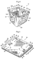
- an airtight container 11 in the present preferred embodiment includes a container unit 12 which contains a plurality of semiconductor wafers W (see FIG. 13) therein; two thin plate supporters 13 which are disposed on side walls opposite to each other inside of the container unit 12 so as to support, on both sides; the semiconductor wafers W contained inside of the container unit 12; a lid 14 which covers the container unit 12; a top flange 15 which is grasped by an arm of a conveyor (not shown) in a factory; and carrying grips 16 which are gripped by a worker when the airtight container 11 is manually carried by the worker.
- the container unit 12 is formed into a cubic shape as a whole.
- the container unit 12 is constituted of four side walls 12A, 12B, 12C and 12D and a bottom plate 12E serving as peripheral walls and has an opening 12F formed at an upper portion thereof in a vertically set state (i.e., in a state shown in FIG. 4).
- a vertically set state i.e., in a state shown in FIG. 4.
- the container unit 12 is laterally set.
- Outside of the side wall 12B serving as a bottom in the laterally set state is disposed a positioning means (not shown) for the airtight container 11.
- Outside of the side wall 12A serving as a top in the laterally set state is detachably attached the top flange 15.
- Outside of the side walls 12C and 12D serving as lateral walls in the laterally set state are detachably attached the carrying grips 16.
- a lid receiver 18, to which the lid 14 is fitted is disposed at an upper end of each of the side walls 12A, 12B, 12C and 12D of the container unit 12 in the vertically set state.
- the lid receiver 18 is formed by enlarging the upper end of the container unit 12 to the dimension of the lid 14.
- the lid 14 is adapted to be fitted to the inside of a vertical plate 18A of the lid receiver 18 and to abut against a horizontal plate 18B, to be thus fixed to the lid receiver 18.
- first fitted portions 20 for fixing the lid 14 onto a side of the container unit 12 in engagement with a locking member of a simplified attaching/detaching mechanism 32, described later.
- the first fitted portion 20 is formed by engraving the vertical plate 18A into a rectangular shape.
- a lid locking member of the simplified attaching/detaching mechanism 32 is designed to be fitted at an upper surface inside of the first fitted portion 20.
- a second fitted portion 21 is formed in the vicinity of each of the first fitted portions 20.
- the second fitted portions 21 are fitted with a simplified attaching/detaching mechanism for the lid, having another structure.
- the lid 14 includes a main body 30, a cover plate (not shown) and the simplified attaching/detaching mechanism 32.
- the main body 30 is a lower plate for covering the lower side, and is formed into a shallow dish of a substantial rectangle.
- An inside plate 30A serving as a bottom plate of the main body 30 and a cover plate serving as an upper plate for covering the upper side of the main body 30 define therein a wide space for supporting the thin plate.
- a gasket receiver 31 Around a lower portion of the main body 30 is secured a gasket receiver 31. At the gasket receiver 31 is received the gasket, which is fitted to the seal groove 18C in a state in which the main body 30 is disposed in the lid receiver 18 of the container unit 12, thereby sealing the inside of the container unit 12.
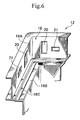
- disposing portions 33 At ends on both sides in a lateral direction in the main body 30 of the lid 14 (i.e., on both sides in upper left and lower right directions in FIG. 5) are provided disposing portions 33, to which the simplified attaching/detaching mechanism 32 is fixed, respectively.
- rotary support shafts 34 At the disposing portion 33 are provided rotary support shafts 34, stoppers 35, locking claws 36, base end lower cams 37, tip cams 38 and the like.
- openings 39 At both ends in a lengthwise direction at the disposing portion 33 (i.e., at both ends in upper right and lower left directions in FIG. 5) are formed openings 39, into or from which the locking members of the simplified attaching/detaching mechanism 32 are inserted or detached.
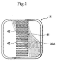
- the support groove 41 is constituted of a slit opened toward the container unit 12 at the inside plate 30A.
- the plurality of elongated support grooves 41 are formed in parallel to each other (in the same number as that of semiconductor wafers W contained inside of the container unit 12).
- the support grooves 41 are located at intervals of the semiconductor wafers W contained inside of the container unit 12. The semiconductor wafers W are fitted into the support grooves 41 one by one, to be thus supported therein.
- a V-shaped groove 42 which positions and supports the semiconductor wafer W fitted with the edge of the semiconductor wafer W.
- the thickness of the inside plate 30A is set according to the depth of the support groove 41.
- a projection protruding according to the depth of the support groove 41 may be formed at the upper surface corresponding to the support groove 41 at the inside plate 30A.
- the airtight container 11 such configured as described above is used in the following manner.
- the semiconductor wafers W are contained inside of the container unit 12, to be then covered with the lid 14.
- the lid 14 is fitted in the lid receiver 18 in the container unit 12, and then, is fixed to the container unit 12 by the simplified attaching/detaching mechanism 32.
- the upper edge of each of the semiconductor wafers W contained inside of the container unit 12 is fitted to the corresponding support groove 41 on the side of the inside plate 30A of the lid 14.
- the upper edge of each of the semiconductor wafers W is fitted to the V-shaped groove 42 at the back of the support groove 41, to be thus fixed and supported in a precisely positioned state.
- the airtight container 11 can produce the following effects:
- the relief groove 62 has a hole formed at the inside plate 30A in the lid 14, to thus allow the plurality of semiconductor wafers W to be inserted. thereinto one by one or every two or more.
- the lateral width of the relief groove 62 is set according to the number of semiconductor wafers W to be inserted.
- the number of relief grooves 62 is determined according to the number of semiconductor wafers W to be contained.
- the relief grooves 62 are formed in parallel to each other in the number such determined as described above. Incidentally, in the case where the plurality of semiconductor wafers W are contained in one relief groove 62, the relief grooves 62 are arranged in parallel to each other in the number accordingly.
- the thin plate supporter 63 is a member for fitting and supporting the semiconductor wafer W inserted through the relief groove 62.
- the thin plate supporter 63 is secured to the cover plate 65 for covering the upper side of the lid 14.
- the thin plate supporter 63 mainly includes a base end supporter 66, an elastic support plate 67, an abutting piece 68, a connecting support plate 69 and a supporting rib 70.
- the semiconductor wafer W is fitted at the edges thereof to two abutting pieces 68, to be thus supported thereby.
- the two abutting pieces 68 are disposed in a manner corresponding to the relief groove 62, and therefore, support one by one the semiconductor wafers W fitted into the relief groove 62.
- the abutting piece 68 is elastically supported on both sides thereof by the elastic support plate 67 and the connecting support plate 69, thereby elastically supporting the semiconductor wafer W.
- the connecting support plate 69 is supported by the supporting rib 70 disposed at the cover plate 65, and therefore, stably supports the two abutting pieces 68. Consequently, the two abutting pieces 68 stably supported by the connecting support plate 69 supported by the supporting rib 70 elastically support the semiconductor wafer W.
- the thin plate supporter 63 may be divided into a plurality of parts. That is to say, the thin plate supporter 63 may be appropriately divided according to fixing modes.
- a seal receiving wall 72 is provided at the inside plate 30A in such a manner as to surround the relief groove 62.
- a hook supporter 73 for supporting the base end supporter 66 of the thin plate supporter 63 is provided at the cover plate 65. The hook supporter 73 faces to the seal receiving wall 72.
- An annular seal 74 is interposed between the hook supporter 73 and the seal receiving wall 72, thereby air-tightly sealing the surroundings of the thin plate supporter 63.
- a space around the thin plate supporter 63 air-tightly sealed by the seal 74 serves as the thin plate support space, which is air-tightly separated from the outside and is opened toward the relief groove 62.
- reference numeral 75 designates another seal for air-tightly sealing a gap defined between the container unit 12 and the lid 14. The two seals 74 and 75 air-tightly seal the inside of the container unit 12 from the outside.
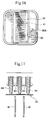
- the seal 74 may be replaced with an elastic film 81, as shown in FIG. 16.
- the elastic film 81 is attached in such a manner as to cover all of the support grooves 41, and then, is fixed via an elastic film presser 82.
- the elastic film 81 may be attached in such a manner as to cover all of the partition plates, as shown in FIGS. 17 and 18.
- An intermediate member 83 and a partition plate 84 shown in FIGS. 17 and 18 are members similar to the intermediate member 55 and the partition plate 56 shown in FIG. 11.
- the elastic film 81 is attached in such a manner as to cover all of the partition plates 84, and then, is fixed via the elastic film presser 82.
- the semiconductor wafer W flexes the elastic film 81, which thus abuts against the intermediate member 83, as shown in FIG. 18. Consequently, the semiconductor wafer W can be elastically supported in the state in which the inside of the container unit 12 is air-tightly sealed.
- the elastic film 81 is made of an expandable synthetic resin in such a manner as to be greatly flexed, as shown in FIG. 18.
- the elastic film 81 is made of polyurethane, a silicone rubber film or the like.
- the elasticity of the elastic film 81 may be adjusted by changing the material or thickness of the elastic film 81, thereby varying force supporting the semiconductor wafer W.
- the force supporting the semiconductor wafer W can be readily changed according to various conditions such as the size or conveyance mode of the semiconductor wafer W by adjusting the elasticity of the elastic film 81. In other words, an optimum supporting force can be readily achieved by adjusting the force supporting the semiconductor wafer W.
- This modification also can produce the same functions and effects as those produced in the above-described preferred embodiment.
Landscapes
- Engineering & Computer Science (AREA)
- Mechanical Engineering (AREA)
- Packaging Frangible Articles (AREA)
- Container, Conveyance, Adherence, Positioning, Of Wafer (AREA)
- Closures For Containers (AREA)
Applications Claiming Priority (1)
| Application Number | Priority Date | Filing Date | Title |
|---|---|---|---|
| JP2005086029A JP2006269771A (ja) | 2005-03-24 | 2005-03-24 | 気密容器 |
Publications (1)
| Publication Number | Publication Date |
|---|---|
| EP1715513A1 true EP1715513A1 (de) | 2006-10-25 |
Family
ID=36636391
Family Applications (1)
| Application Number | Title | Priority Date | Filing Date |
|---|---|---|---|
| EP06006044A Withdrawn EP1715513A1 (de) | 2005-03-24 | 2006-03-23 | Ein luftdicher Behälter |
Country Status (6)
| Country | Link |
|---|---|
| US (1) | US20060213796A1 (de) |
| EP (1) | EP1715513A1 (de) |
| JP (1) | JP2006269771A (de) |
| KR (1) | KR20060103149A (de) |
| CN (1) | CN1836983A (de) |
| TW (1) | TW200711026A (de) |
Families Citing this family (16)
| Publication number | Priority date | Publication date | Assignee | Title |
|---|---|---|---|---|
| JP4584023B2 (ja) * | 2005-05-17 | 2010-11-17 | 信越ポリマー株式会社 | 基板収納容器及びその製造方法 |
| JP4896053B2 (ja) * | 2008-02-27 | 2012-03-14 | ミライアル株式会社 | ウェハ収納容器 |
| US7971722B2 (en) * | 2008-08-08 | 2011-07-05 | Gudeng Precision Industral Co, Ltd | Wafer container with restrainer |
| CN102362340B (zh) * | 2009-05-13 | 2013-12-25 | 未来儿株式会社 | 半导体晶片收纳容器 |
| US20110259840A1 (en) * | 2010-04-23 | 2011-10-27 | Advanced Semiconductor Engineering, Inc. | Semiconductor package magazine |
| US8727278B2 (en) * | 2010-07-16 | 2014-05-20 | The Boeing Company | Article retention device |
| US9181035B2 (en) * | 2011-04-29 | 2015-11-10 | Kyoraku Co., Ltd. | Rectangular thin panel conveyance unit |
| CN102431723A (zh) * | 2011-09-30 | 2012-05-02 | 常熟市华海电子有限公司 | 一种便于芯片盛放的层夹板 |
| KR20150066540A (ko) * | 2012-10-12 | 2015-06-16 | 미라이얼 가부시키가이샤 | 기판 수납 용기 |
| JP6258069B2 (ja) * | 2014-02-26 | 2018-01-10 | 信越ポリマー株式会社 | 基板収納容器 |
| WO2016046985A1 (ja) * | 2014-09-26 | 2016-03-31 | ミライアル株式会社 | 基板収納容器 |
| JP6375577B2 (ja) * | 2015-03-30 | 2018-08-22 | 信越ポリマー株式会社 | 基板収納容器 |
| JP6396255B2 (ja) * | 2015-05-14 | 2018-09-26 | 信越ポリマー株式会社 | 基板収納容器 |
| WO2017136743A1 (en) * | 2016-02-05 | 2017-08-10 | Entegris, Inc. | Cushion retainer for substrate container |
| KR20250019627A (ko) * | 2022-05-31 | 2025-02-10 | 미라이얼 가부시키가이샤 | 기판수납용기 및 뚜껑측 기판지지부 |
| CN116884894B (zh) * | 2023-09-07 | 2023-11-28 | 苏州鸿安机械股份有限公司 | 一种晶圆生产装载设备 |
Citations (3)
| Publication number | Priority date | Publication date | Assignee | Title |
|---|---|---|---|---|
| US5255797A (en) * | 1992-02-26 | 1993-10-26 | Fluoroware, Inc. | Wafer carrier with wafer retaining cushions |
| US6267245B1 (en) * | 1998-07-10 | 2001-07-31 | Fluoroware, Inc. | Cushioned wafer container |
| US20030221985A1 (en) * | 2001-05-30 | 2003-12-04 | Toshitsugu Yajima | Precision substrate storage container and retaining member therefor |
Family Cites Families (1)
| Publication number | Priority date | Publication date | Assignee | Title |
|---|---|---|---|---|
| US6736268B2 (en) * | 1997-07-11 | 2004-05-18 | Entegris, Inc. | Transport module |
-
2005
- 2005-03-24 JP JP2005086029A patent/JP2006269771A/ja active Pending
-
2006
- 2006-02-21 TW TW095105718A patent/TW200711026A/zh unknown
- 2006-03-07 CN CNA2006100572152A patent/CN1836983A/zh active Pending
- 2006-03-14 US US11/374,139 patent/US20060213796A1/en not_active Abandoned
- 2006-03-22 KR KR1020060026140A patent/KR20060103149A/ko not_active Withdrawn
- 2006-03-23 EP EP06006044A patent/EP1715513A1/de not_active Withdrawn
Patent Citations (3)
| Publication number | Priority date | Publication date | Assignee | Title |
|---|---|---|---|---|
| US5255797A (en) * | 1992-02-26 | 1993-10-26 | Fluoroware, Inc. | Wafer carrier with wafer retaining cushions |
| US6267245B1 (en) * | 1998-07-10 | 2001-07-31 | Fluoroware, Inc. | Cushioned wafer container |
| US20030221985A1 (en) * | 2001-05-30 | 2003-12-04 | Toshitsugu Yajima | Precision substrate storage container and retaining member therefor |
Also Published As
| Publication number | Publication date |
|---|---|
| TW200711026A (en) | 2007-03-16 |
| KR20060103149A (ko) | 2006-09-28 |
| CN1836983A (zh) | 2006-09-27 |
| US20060213796A1 (en) | 2006-09-28 |
| JP2006269771A (ja) | 2006-10-05 |
Similar Documents
| Publication | Publication Date | Title |
|---|---|---|
| EP1715513A1 (de) | Ein luftdicher Behälter | |
| US8322533B2 (en) | Lid body for substrate storage container and substrate storage container | |
| EP1341226B1 (de) | Abdichtelement und substratspeicherbehälter mit dem abdichtelement | |
| US8528738B2 (en) | Reusable resilient cushion for wafer container | |
| US11161648B2 (en) | Panel storage container | |
| KR20060052189A (ko) | 수납 용기 | |
| MY131620A (en) | Wafer enclosure sealing arrangement for wafer containers | |
| JP2000315721A (ja) | 基板収納容器の識別構造及び基板収納容器の識別方法 | |
| TW448531B (en) | Thin-plate accommodating/transporting container | |
| JPH0945759A (ja) | パッケージ | |
| JP2003222992A (ja) | マスクケース | |
| CN109075112A (zh) | 用于衬底容器的缓冲保持器 | |
| JP7467367B2 (ja) | パネル収納容器 | |
| CN218827019U (zh) | 一种单片晶圆盒 | |
| JP4204284B2 (ja) | 基板収納容器 | |
| KR102942671B1 (ko) | 기판수납용기 및 그 뚜껑 | |
| JPH11154699A (ja) | 容器の封止構造 | |
| JP7380526B2 (ja) | シールガスケットの取り付け方法 | |
| KR200319007Y1 (ko) | 웨이퍼 수납용기의 기밀구조 | |
| JPH11154699A5 (de) | ||
| JP2007142192A (ja) | 薄板体収納容器 | |
| WO2026083709A1 (ja) | 基板収納容器 | |
| JP3856503B2 (ja) | 精密基板の収納容器および該収納容器を用いた収納方法 | |
| WO2024241560A1 (ja) | 基板収納容器 | |
| WO2026083716A1 (ja) | 基板収納容器 |
Legal Events
| Date | Code | Title | Description |
|---|---|---|---|
| PUAI | Public reference made under article 153(3) epc to a published international application that has entered the european phase |
Free format text: ORIGINAL CODE: 0009012 |
|
| AK | Designated contracting states |
Kind code of ref document: A1 Designated state(s): AT BE BG CH CY CZ DE DK EE ES FI FR GB GR HU IE IS IT LI LT LU LV MC NL PL PT RO SE SI SK TR |
|
| AX | Request for extension of the european patent |
Extension state: AL BA HR MK YU |
|
| 17P | Request for examination filed |
Effective date: 20070418 |
|
| 17Q | First examination report despatched |
Effective date: 20070518 |
|
| AKX | Designation fees paid |
Designated state(s): DE |
|
| STAA | Information on the status of an ep patent application or granted ep patent |
Free format text: STATUS: THE APPLICATION IS DEEMED TO BE WITHDRAWN |
|
| 18D | Application deemed to be withdrawn |
Effective date: 20080327 |