EP1715568A2 - Konstantspannungsschaltung mit möglicher Verkürzung der Startzeit, Halbleitervorrichtung mit dieser Schaltung sowie Steuerungsmethode der Schaltung - Google Patents
Konstantspannungsschaltung mit möglicher Verkürzung der Startzeit, Halbleitervorrichtung mit dieser Schaltung sowie Steuerungsmethode der Schaltung Download PDFInfo
- Publication number
- EP1715568A2 EP1715568A2 EP06252072A EP06252072A EP1715568A2 EP 1715568 A2 EP1715568 A2 EP 1715568A2 EP 06252072 A EP06252072 A EP 06252072A EP 06252072 A EP06252072 A EP 06252072A EP 1715568 A2 EP1715568 A2 EP 1715568A2
- Authority
- EP
- European Patent Office
- Prior art keywords
- voltage
- output
- switching
- regulator
- circuit
- Prior art date
- Legal status (The legal status is an assumption and is not a legal conclusion. Google has not performed a legal analysis and makes no representation as to the accuracy of the status listed.)
- Withdrawn
Links
Images

Classifications
-
- H—ELECTRICITY
- H02—GENERATION; CONVERSION OR DISTRIBUTION OF ELECTRIC POWER
- H02M—APPARATUS FOR CONVERSION BETWEEN AC AND AC, BETWEEN AC AND DC, OR BETWEEN DC AND DC, AND FOR USE WITH MAINS OR SIMILAR POWER SUPPLY SYSTEMS; CONVERSION OF DC OR AC INPUT POWER INTO SURGE OUTPUT POWER; CONTROL OR REGULATION THEREOF
- H02M1/00—Details of apparatus for conversion
- H02M1/36—Means for starting or stopping converters
-
- H—ELECTRICITY
- H02—GENERATION; CONVERSION OR DISTRIBUTION OF ELECTRIC POWER
- H02M—APPARATUS FOR CONVERSION BETWEEN AC AND AC, BETWEEN AC AND DC, OR BETWEEN DC AND DC, AND FOR USE WITH MAINS OR SIMILAR POWER SUPPLY SYSTEMS; CONVERSION OF DC OR AC INPUT POWER INTO SURGE OUTPUT POWER; CONTROL OR REGULATION THEREOF
- H02M3/00—Conversion of DC power input into DC power output
- H02M3/02—Conversion of DC power input into DC power output without intermediate conversion into AC
- H02M3/04—Conversion of DC power input into DC power output without intermediate conversion into AC by static converters
- H02M3/10—Conversion of DC power input into DC power output without intermediate conversion into AC by static converters using discharge tubes with control electrode or semiconductor devices with control electrode
- H02M3/145—Conversion of DC power input into DC power output without intermediate conversion into AC by static converters using discharge tubes with control electrode or semiconductor devices with control electrode using devices of a triode or transistor type requiring continuous application of a control signal
- H02M3/155—Conversion of DC power input into DC power output without intermediate conversion into AC by static converters using discharge tubes with control electrode or semiconductor devices with control electrode using devices of a triode or transistor type requiring continuous application of a control signal using semiconductor devices only
-
- G—PHYSICS
- G05—CONTROLLING; REGULATING
- G05F—SYSTEMS FOR REGULATING ELECTRIC OR MAGNETIC VARIABLES
- G05F1/00—Automatic systems in which deviations of an electric quantity from one or more predetermined values are detected at the output of the system and fed back to a device within the system to restore the detected quantity to its predetermined value or values, i.e. retroactive systems
- G05F1/10—Regulating voltage or current
- G05F1/46—Regulating voltage or current wherein the variable actually regulated by the final control device is DC
- G05F1/56—Regulating voltage or current wherein the variable actually regulated by the final control device is DC using semiconductor devices in series with the load as final control devices
-
- H—ELECTRICITY
- H02—GENERATION; CONVERSION OR DISTRIBUTION OF ELECTRIC POWER
- H02M—APPARATUS FOR CONVERSION BETWEEN AC AND AC, BETWEEN AC AND DC, OR BETWEEN DC AND DC, AND FOR USE WITH MAINS OR SIMILAR POWER SUPPLY SYSTEMS; CONVERSION OF DC OR AC INPUT POWER INTO SURGE OUTPUT POWER; CONTROL OR REGULATION THEREOF
- H02M3/00—Conversion of DC power input into DC power output
- H02M3/02—Conversion of DC power input into DC power output without intermediate conversion into AC
- H02M3/04—Conversion of DC power input into DC power output without intermediate conversion into AC by static converters
- H02M3/10—Conversion of DC power input into DC power output without intermediate conversion into AC by static converters using discharge tubes with control electrode or semiconductor devices with control electrode
- H02M3/145—Conversion of DC power input into DC power output without intermediate conversion into AC by static converters using discharge tubes with control electrode or semiconductor devices with control electrode using devices of a triode or transistor type requiring continuous application of a control signal
- H02M3/155—Conversion of DC power input into DC power output without intermediate conversion into AC by static converters using discharge tubes with control electrode or semiconductor devices with control electrode using devices of a triode or transistor type requiring continuous application of a control signal using semiconductor devices only
- H02M3/156—Conversion of DC power input into DC power output without intermediate conversion into AC by static converters using discharge tubes with control electrode or semiconductor devices with control electrode using devices of a triode or transistor type requiring continuous application of a control signal using semiconductor devices only with automatic control of output voltage or current, e.g. switching regulators
-
- H—ELECTRICITY
- H02—GENERATION; CONVERSION OR DISTRIBUTION OF ELECTRIC POWER
- H02M—APPARATUS FOR CONVERSION BETWEEN AC AND AC, BETWEEN AC AND DC, OR BETWEEN DC AND DC, AND FOR USE WITH MAINS OR SIMILAR POWER SUPPLY SYSTEMS; CONVERSION OF DC OR AC INPUT POWER INTO SURGE OUTPUT POWER; CONTROL OR REGULATION THEREOF
- H02M1/00—Details of apparatus for conversion
- H02M1/0045—Converters combining the concepts of switch-mode regulation and linear regulation, e.g. linear pre-regulator to switching converter, linear and switching converter in parallel, same converter or same transistor operating either in linear or switching mode
Definitions
- the present invention relates to a constant-voltage circuit, a semiconductor apparatus including the constant-voltage circuit, and a method of controlling the constant-voltage circuit, and more particularly to a constant-voltage circuit including a soft-start function capable of reducing time required for starting, a semiconductor apparatus including the constant-voltage circuit, and a method of controlling the constant-voltage circuit.
- a general method of reducing electricity consumption of electronic equipment is to keep the electronic equipment in a stand-by state while the electronic equipment is not operating so that operation of a circuit therein is stopped to cut electricity consumption.
- bringing the electronic equipment into the stand-by state may not achieve satisfactory electricity saving when the power supply circuit is not efficient.
- General power supply circuits used in electronic equipment include a switching regulator and a series regulator.
- the switching regulator is highly efficient with a rated load, the switching regulator has a large output voltage ripple and large operating noise, and internally consumes a relatively large amount of electricity. Therefore, the switching regulator significantly impairs efficiency under light load with a small output current. Further, the switching regulator requires a relatively long time for a rise of an output voltage after the power is turned on, and takes a relatively long time for responding to shifts in an input voltage and a load. Therefore, the switching regulator is defective in that the switching regulator has low stability of an output voltage.
- the series regulator has low efficiency with a large amount of load current as an output transistor consumes a large amount of electricity
- the series regulator has a small output voltage ripple and small operating noise, and a power supply control circuit internally consumes a small amount of electricity. Therefore, the series regulator may achieve higher efficiency than the switching regulator with a small amount of load current. Further, it is easy in the series regulator to reduce amounts of time required for a rise of an output voltage and for responding to shifts in an input voltage and a load. Further, the series regulator has high stability of an output voltage.
- a background power supply circuit includes both a switching regulator and a series regulator, and selectively uses one of the switching and series regulators according to electricity consumption so as to improve efficiency of a constant-voltage circuit.
- FIG. 1 illustrates a configuration of the constant-voltage circuit.
- a constant-voltage circuit 101 includes a switching regulator 102, a series regulator 103, and a control circuit unit 104.
- the switching regulator 102 and the series regulator 103 convert voltages input from a direct current power supply 110 to respective voltages.
- the control circuit unit 104 controls a switching operation for switching between the switching regulator 102 and the series regulator 103 so as to selectively operate one of the switching regulator 102 and the series regulator 103 according to a switch control signal Sc input from outside.
- the control circuit unit 104 firstly causes both the switching regulator 102 and the series regulator 103 to operate, and then causes a desired one of the switching regulator 102 and the series regulator 103 to continue operating.
- a general switching regulator includes a soft-start circuit for gradually raising an output voltage so that an excessive current does not flow into a switching transistor on startup.
- An example of the soft-start circuit gradually increases a reference voltage.
- Another example of the soft-start circuit uses a D/A converter to gradually increase a reference voltage.
- This patent specification describes a constant-voltage circuit, including a switching regulator including a function for performing a soft-start operation for raising an output voltage to a rated voltage at a constant speed when starting operation, configured to start operating according to a selection signal, and to convert an input voltage input to an input terminal to the rated voltage to output to an output terminal, and a series regulator including a function for regulating a current so that an output current does not exceed a predetermined value, configured to start operating according to the selection signal, and to convert the input voltage to the rated voltage to output to the output terminal.
- the series regulator simultaneously starts operating when the switching regulator starts operating, and automatically stops outputting a current to the output terminal when the soft-start operation of the switching regulator is completed.
- the selection signal is input from outside for exclusively causing one of the switching regulator and the series regulator to operate.
- This patent specification further describes a semiconductor apparatus provided with a predetermined function, including a constant-voltage circuit which includes a switching regulator including a function for performing a soft-start operation for raising an output voltage to a rated voltage at a constant speed when starting operation, configured to start operating according to a selection signal, and to convert an input voltage input to an input terminal to the rated voltage to output, and a series regulator including a function for regulating a current so that an output current does not exceed a predetermined value, configured to start operating according to the selection signal, and to convert the input voltage to the rated voltage to output.
- the series regulator simultaneously starts operating when the switching regulator starts operating, and automatically stops outputting a current when the soft-start operation of the switching regulator is completed.
- the selection signal is input from outside for exclusively causing one of the switching regulator and the series regulator to operate.
- This patent specification further describes a method of controlling a constant-voltage circuit including a function of performing a soft-start operation, which includes the steps of providing a switching regulator including the function of performing the soft-start operation and a series regulator, receiving a selection signal from outside for exclusively causing one of the switching regulator and the series regulator to operate, simultaneously activating the series regulator when the switching regulator starts operating, and causing the series regulator to automatically stop outputting a current to an output terminal when the soft-start operation of the switching regulator is completed.
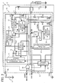
- a constant-voltage circuit 1 includes a switching regulator 2 and a series regulator 3.
- the switching regulator 2 includes a smoothing circuit unit and a switching control circuit unit.
- the switching regulator 2 further includes a switching transistor M1, a resistor R1, a resistor R2, a NMOS transistor M3, and an AND circuit 18.
- the smoothing circuit unit includes a switching transistor M2, a smoothing inductor L1, and a condenser C1.
- the switching control circuit unit includes a first reference voltage generation circuit 11, a first error amplification circuit 12, a triangular wave generation circuit 13, a PWM comparison circuit 14, an output control circuit 15, a first output current regulation circuit 16, and a soft-start circuit 17.
- the series regulator 3 includes an output voltage detection circuit unit and a control circuit unit.
- the series regulator 3 further includes a second reference voltage generation circuit 21, a second error amplification circuit 22, and a second output current regulation circuit 23.
- the output voltage detection circuit unit includes a resistor R3, a resistor R4, an output transistor M4, and a NMOS transistor M5.
- the control circuit unit includes a TR control circuit 24.
- the constant-voltage circuit 1 converts an input voltage Vin input to an input terminal IN from a direct current (DC) power source 5 such as a battery to a predetermined constant voltage to output from an output terminal OUT as an output voltage Vout.
- the output terminal OUT is connected to a ground voltage through a load 6 so as to provide the load 6 with the output voltage Vout.
- the switching regulator 2 converts the input voltage Vin to a predetermined voltage to output from the output terminal OUT as an output voltage Vo1.
- the series regulator 3 converts the input voltage Vin to a predetermined voltage to output from the output terminal OUT as an output voltage Vo2.
- the switching transistor M1 includes a PMOS transistor for controlling an output level of the input voltage Vin input to the input terminal IN.
- the switching transistor M2 includes a NMOS transistor for synchronization and rectification.
- the resistors R1 and R2 branch the output voltage Vout to generate and output a first branched voltage VFB1 for output voltage detection.
- the resistors R1 and R2 are included in a series circuit of which end is connected to the output terminal OUT. Another end of the series circuit is connected to a ground voltage under the control of the NMOS transistor M3. In other words, the NMOS transistor M3 controls the connection of the series circuit to the ground voltage.
- the first reference voltage generation circuit 11 generates and outputs a first reference voltage Vr1 according to an input signal.
- the first error amplification circuit 12 amplifiers and outputs a difference between the first branched voltage VFB1 and the first reference voltage Vr1.
- the triangular wave generation circuit 13 generates and outputs a predetermined triangular wave signal TW.
- the PWM comparison circuit 14 compares an output voltage Ver from the first error amplification circuit 12 with the triangular wave signal TW from the triangular wave generation circuit 13, and generates and outputs a pulse signal Spw for controlling pulse width modulation so that a pulse width according to the output voltage Ver is obtained.
- the output control circuit 15 generates a control signal PD for controlling switching of the switching transistor M1 to drive the switching transistor M1, and generates a control signal ND for controlling switching of the switching transistor M2 to drive the switching transistor M2.
- the first output current regulation circuit 16 detects a voltage drop when the switching transistor M1 is turned on, and causes the output control circuit 15 to turn off the switching transistor M1 and the switching transistor M2 when an output current from the switching transistor M1 exceeds a predetermined current.
- the soft-start circuit 17 gradually increases the first reference voltage Vr1 when the switching regulator 2 is started so that an excessive current does not flow into the switching transistor M1.
- the AND circuit 18 includes an input terminal in which a mode signal MODE is input from outside, and another input terminal in which a chip enable signal CE is input from outside.
- the second reference voltage generation circuit 21 generates and outputs a predetermined second reference voltage Vr2.
- the resistors R3 and R4 branch the output voltage Vout to generate and output a second branched voltage VFB2 for output voltage detection.
- the resistors R3 and R4 are included in a series circuit of which end is connected to the output terminal OUT. Another end of the series circuit is connected to a ground voltage under the control of the NMOS transistor M5. In other words, the NMOS transistor M5 controls the connection of the series circuit to the ground voltage.
- the output transistor M4 includes a PMOS transistor for controlling a current to be output to the output terminal OUT according to a signal input to a gate.
- the second error amplification circuit 22 controls operation of the output transistor M4 so that the second branched voltage VFB2 becomes equal to the second reference voltage Vr2.
- the second output current regulation circuit 23 controls operation of the output transistor M4 to regulate a current output from the output transistor M4 when the current becomes equal to or exceeds a predetermined value.
- the TR control circuit 24 controls operation of the NMOS transistor M5.
- the above circuits except the smoothing inductor L1 and the condenser C1 of the switching regulator 2 are integrated into a single integrated circuit (hereinafter referred to as IC).
- the IC includes the input terminal IN, the output terminal OUT, a Lx terminal, a GND terminal, a MODE terminal, and a CE terminal.
- the GND terminal is connected to a ground voltage.
- the MODE terminal receives the mode signal MODE from outside.
- the CE terminal receives the chip enable signal CE from outside.
- the load 6 may be integrated into the IC when the load 6 includes an integratable circuit, and the mode signal MODE may include a selection signal.
- the switching transistor M1 and the switching transistor M2 are serially connected between the input terminal IN and the ground voltage.
- a connection part of the switching transistor M1 and the switching transistor M2 is connected to the Lx terminal.
- the smoothing inductor L1 is arranged between the Lx terminal and the output terminal OUT, and is connected thereto.
- the condenser C1 is arranged between the output terminal OUT and a ground voltage, and is connected thereto.
- a serial circuit including the resistors R1 and R2, and the NMOS transistor M3 is arranged between the output terminal OUT and the GND terminal, and is connected thereto.
- a connection part between the resistors R1 and R2 is connected to an inverting input terminal of the first error amplification circuit 12.
- the first reference voltage Vr1 is input to a non-inverting input terminal of the first error amplification circuit 12.
- the output voltage Ver of the first error amplification circuit 12 is input to an inverting input terminal of a comparator included in the PWM comparison circuit 14.
- the triangular wave signal TW from the triangular wave generation circuit 13 is input to a non-inverting input terminal of the comparator.
- a pulse signal Spw from the PWM comparison circuit 14 is output to each of the output control circuit 15 and the first output current regulation circuit 16.
- the output control circuit 15 outputs the control signal PD for controlling switching of the switching transistor M1 to a gate of the switching transistor M1, and outputs the control signal ND for controlling switching of the switching transistor M2 to a gate of the switching transistor M2.
- the first reference voltage generation circuit 11 receives a signal SS1 from the soft-start circuit 17, and generates and outputs the first reference voltage Vr1 according to the signal SS1.
- the AND circuit 18 outputs an output signal to each gate of the first reference voltage generation circuit 11, the first error amplification circuit 12, the triangular wave generation circuit 13, the PWM comparison circuit 14, the first output current regulation circuit 16, the soft-start circuit 17, and the NMOS transistor M3.
- the output transistor M4 is arranged between the input terminal IN and the output terminal OUT, and is connected thereto. Further, the resistors R3 and R4, and the NMOS transistor M5 are serially arranged between the output terminal OUT and the GND terminal, and are connected thereto.
- An inverting input terminal of the second error amplification circuit 22 receives the second branched voltage VFB2.
- An output terminal of the second error amplification circuit 22 is connected to a gate of the output transistor M4.
- the chip enable signal CE input to the CE terminal is input to each of the second reference voltage generation circuit 21, the second error amplification circuit 22, the second output current regulation circuit 23, and the TR control circuit 24.
- the TR control circuit 24 receives the mode signal MODE, and further receives an operation completion signal SSE from the soft-start circuit 17. Further, the TR control circuit 24 is connected to a gate of the NMOS transistor M5 to control operation of the NMOS transistor M5 according to the chip enable signal CE and the operation completion signal SSE.
- the output voltage Vo1 is equal to the output voltage Vout
- the output voltage Vo1 represents a target voltage output from the switching regulator 2, and is not necessarily equal to the output voltage Vout.
- the output voltage Vo2 of the series regulator 3 is equal to the output voltage Vout
- the output voltage Vo2 represents a target voltage output from the series regulator 3, and is not necessarily equal to the output voltage Vout.
- the constant-voltage circuit 1 having the above configuration, when a level of the chip enable signal CE becomes low, a level of the output terminal of the AND circuit 18 becomes low regardless of the mode signal MODE. Further, in the case, the first reference voltage generation circuit 11, the first error amplification circuit 12, the triangular wave generation circuit 13, the PWM comparison circuit 14, the first output current regulation circuit 16, and the soft-start circuit 17 in the switching regulator 2 stop operating, and the NMOS transistor M3 is turned off and brought into a cutoff state. Further, when the first output current regulation circuit 16 stops operating, the output regulation circuit 15 also stops operating. As a result, output of the control signals PD and ND is stopped.
- the switching transistors M1 and M2 are each turned off and brought into the cutoff state, thereby causing the switching regulator 2 to stop operating. Further, when the level of the chip enable signal CE becomes low, the second reference voltage generation circuit 21, the second error amplification circuit 22, the second output current regulation circuit 23, and the TR control circuit 24 in the series regulator 3 stop operating. Since the TR control circuit 24 stops operating, the NMOS transistor M5 is turned off and brought into the cutoff state. As a result, the output transistor M4 is turned off and brought into the cutoff state, and the series regulator 3 stops operating.
- the second reference voltage generation circuit 21 the second error amplification circuit 22, the second output current regulation circuit 23, and the TR control circuit 24 in the series regulator 3 start operating regardless of the mode signal MODE.
- the mode signal MODE selectively causes one of the switching regulator 2 and the series regulator 3 to operate.
- the level of the mode signal MODE becomes high when to cause the switching regulator 2 to operate, and becomes low when to cause the series regulator 3 to operate.
- the level of the AND circuit 18 becomes high, the first reference voltage generation circuit 11, and first error amplification circuit 12, the triangular wave generation circuit 13, the PWM comparison circuit 14, the first output current regulation circuit 16, and the soft-start circuit 17 of the switching regulator 2 start operating, and the switching regulator 2 starts operating.
- the switching transistor M1 performs a switching operation.
- the smoothing inductor L1 is supplied with a current.
- the switching transistor M2 is off.
- the switching transistor M1 is turned off, the switching transistor M2 is turned on, and energy accumulated in the smoothing inductor L1 is released through switching transistor M2.
- the current generated at the time is smoothed by the condenser C1, and is output to the load 6 through the output terminal OUT.
- the output voltage Vout output from the output terminal OUT is branched by the resistors R1 and R2 for detecting output voltages, and the first branched voltage VFB1 is input to the inverting input terminal of the first error amplification circuit 12.
- the output voltage Ver of the first error amplification circuit 12 decreases, and a duration of a duty cycle of the pulse signal Spw from the PWM comparison circuit 14 becomes shorter. As a result, a period of time in which the switching transistor M1 is on becomes shorter, and the switching regulator 2 is controlled to reduce the output voltage Vo1.
- the output voltage Vo1 of the switching regulator 2 increases, and the duration of the duty cycle of the pulse signal Spw from the PWM comparison circuit 14 becomes longer. As a result, the period of time in which the switching transistor M1 is on becomes longer, and the switching regulator 2 is controlled so that the output voltage Vo1 has a value corresponding to the first reference voltage Vr1.
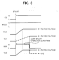
- FIG. 3 is a timing chart showing an exemplary waveform of each of the signals shown in FIG. 2. Operation of the soft-start circuit 17 is described in detail below referring to FIG. 3. Alternate long and short dashed lines indicate differences from the output voltage Vout as described before.
- the soft-start circuit 17 starts operating.
- the soft-start circuit 17 gradually increases the first reference voltage Vr1 by using the control signal SS1 until the output voltage Vo1 shifts to a predetermined rated voltage.
- the output voltage Vo1 of the switching regulator gradually increases until the output voltage Vo1 becomes equal to the predetermined rated-voltage as indicated by the alternate long and short dashed line in order to gradually increase the first reference voltage Vr1.
- the soft-start circuit 17 performs controlling so that an excessive current does not flow into the switching transistor M1.
- the soft-start circuit 17 keeps the operation completion signal SSE at a high level.
- the soft-start circuit 17 keeps the operation completion signal SSE at a low level.
- the series regulator 3 starts operating when the level of the chip enable signal CE becomes high. In other words, when the switching regulator 2 is operating, the series regulator 3 is also operating. At the time, the TR control circuit 24 turns off the NMOS transistor M5 to bring into the cutoff state when the operation completion signal SSE is kept at the low level. Further, the level of the output signal of the AND circuit 18 becomes low, and the switching regulator 2 stops operating. In other words, when the level of the mode signal MODE becomes low, the TR control circuit 24 turns on the NMOS transistor M5 to bring into conduction regardless of the operation completion signal SSE from the soft-start circuit 17.
- the TR control circuit 24 turns on the NMOS transistor M5, as described above, regardless of the operation completion signal SSE from the soft-start circuit 17 when the level of the chip enable signal CE is high and the level of the mode signal MODE is low. Further, the TR control circuit 24 turns on the NMOS transistor M5 only in a case the operation completion signal SSE from the soft-start circuit 17 is at the high level when the level of the chip enable signal CE is high and the level of the mode signal MODE is high. Further, the TR control circuit 24 turns off the NMOS transistor M5 regardless of the operation completion signal SSE from the soft-start circuit 17 when the level of the chip enable signal CE is low.
- the second error amplification circuit 22 amplifies a difference between the second reference voltage Vr2 and the second branched voltage VFB2, and outputs the difference to the gate of the output transistor M4 to control operation of the output transistor M4 so that the output voltage Vo2 becomes equal to the predetermined rated voltage.
- the output voltage Vo2 becomes equal to the second reference voltage Vr2 which is smaller than the predetermined rated voltage.
- the series regulator 3 starts operating immediately after the level of the chip enable signal CE becomes high, and, as a result, the output voltage Vo2 satisfies the above expression 1. Therefore, in the series regulator 3, a rise property of the output voltage Vout can be synchronized to a rise of the output voltage Vo2 of the series regulator 3 as shown in FIG. 3 since the condenser C1 connected to the output terminal OUT is charged with a current having a value regulated by the second output current regulation circuit 23 to raise the output voltage Vo2, and a time constant to be determined by the value of the current regulated by the second output current regulation circuit 23 and capacity of the condenser C1 is set such that the time constant is shorter than a duration of the soft-start operation. As a result, a length of time required for starting the constant-voltage circuit 2 can be reduced.
- the TR control circuit 24 turns off the NMOS transistor M5.
- the output voltage Vo2 of the series regulator 3 becomes equal to the second reference voltage Vr2 as indicated by the alternate long and short dashed line shown in FIG. 3, since the output voltage Vout has been increased to the rated voltage by the output voltage Vo1 of the switching regulator 2, the level of the output signal of the second error amplification circuit 22 becomes high, and as a result, turns off the output transistor M4.
- the series regulator 3 does not output any current, and electric power is supplied to the load 6 only from the switching regulator 2.
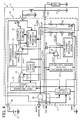
- a flywheel diode D1 may be used as shown in FIG. 4 instead of the switching transistor M2 shown in FIG. 2.
- the same reference numeral as the reference numeral in FIG. 2 represents the same component.
- the flywheel diode D1 is arranged outside the IC, the flywheel diode D1 is formed inside the IC when the flywheel diode D1 includes a diode suitable for integration, such as a PN junction type.
- the flywheel diode D1, the smoothing inductor L1, and the condenser C1 are included in a smoothing circuit unit.
- the switching regulator 2 and the series regulator 3 are simultaneously activated on startup, and the output voltage Vout is risen within a time period determined by the current regulated by the second output current regulation circuit 23 of the series regulator 3 and the time constant of the condenser C1 even when the soft-start circuit 17 takes a long operation period, the output voltage Vout can be risen to the rated voltage in a short time. Further, since the switching regulator 2 rises the output voltage Vo1 by using the soft-start circuit 17, the switching transistor M1 can be prevented from receiving an excessive current. As a result, the output voltage can be safely risen in a short time.
- the constant-voltage circuit 1 may be used in a semiconductor apparatus (not shown).
Landscapes
- Engineering & Computer Science (AREA)
- Power Engineering (AREA)
- Physics & Mathematics (AREA)
- Electromagnetism (AREA)
- General Physics & Mathematics (AREA)
- Radar, Positioning & Navigation (AREA)
- Automation & Control Theory (AREA)
- Dc-Dc Converters (AREA)
- Continuous-Control Power Sources That Use Transistors (AREA)
Applications Claiming Priority (1)
| Application Number | Priority Date | Filing Date | Title |
|---|---|---|---|
| JP2005123696A JP4570507B2 (ja) | 2005-04-21 | 2005-04-21 | 定電圧回路、定電圧回路を備えた半導体装置及び定電圧回路の制御方法 |
Publications (2)
| Publication Number | Publication Date |
|---|---|
| EP1715568A2 true EP1715568A2 (de) | 2006-10-25 |
| EP1715568A3 EP1715568A3 (de) | 2010-01-27 |
Family
ID=36589342
Family Applications (1)
| Application Number | Title | Priority Date | Filing Date |
|---|---|---|---|
| EP06252072A Withdrawn EP1715568A3 (de) | 2005-04-21 | 2006-04-13 | Konstantspannungsschaltung mit möglicher Verkürzung der Startzeit, Halbleitervorrichtung mit dieser Schaltung sowie Steuerungsmethode der Schaltung |
Country Status (6)
| Country | Link |
|---|---|
| US (1) | US7579817B2 (de) |
| EP (1) | EP1715568A3 (de) |
| JP (1) | JP4570507B2 (de) |
| KR (1) | KR100756615B1 (de) |
| CN (1) | CN100452629C (de) |
| TW (1) | TWI419454B (de) |
Families Citing this family (13)
| Publication number | Priority date | Publication date | Assignee | Title |
|---|---|---|---|---|
| JP4978283B2 (ja) * | 2007-04-10 | 2012-07-18 | セイコーエプソン株式会社 | モータ駆動制御回路、半導体装置、電子時計および発電装置付き電子時計 |
| TWI352268B (en) * | 2007-11-28 | 2011-11-11 | Realtek Semiconductor Corp | Apparatus and method for hybrid regulator |
| JP5091027B2 (ja) * | 2008-06-25 | 2012-12-05 | 株式会社リコー | スイッチングレギュレータ |
| US9093993B2 (en) * | 2008-07-31 | 2015-07-28 | System General Corp. | Power saving circuit for PWM circuit |
| JP4853511B2 (ja) * | 2008-12-04 | 2012-01-11 | 株式会社デンソー | スイッチング電源回路 |
| US7990196B2 (en) * | 2009-12-22 | 2011-08-02 | Toshiba America Electronic Components, Inc. | Signal driver with first pulse boost |
| KR20110106669A (ko) * | 2010-03-23 | 2011-09-29 | 삼성전자주식회사 | 고전압 전원 장치 |
| JP2012196050A (ja) * | 2011-03-16 | 2012-10-11 | Sanken Electric Co Ltd | ソフトスタート回路 |
| CN103529890B (zh) * | 2012-07-06 | 2016-08-03 | 国民技术股份有限公司 | 一种软启动装置及方法 |
| GB2508418A (en) * | 2012-11-30 | 2014-06-04 | Control Tech Ltd | Thyristor rectifier charge rate controller |
| CN104753331B (zh) * | 2015-04-21 | 2017-11-03 | 中国电子科技集团公司第三十八研究所 | 一种大功率发射机软启动装置及其软启动方法 |
| JP6836150B2 (ja) * | 2017-01-20 | 2021-02-24 | セイコーエプソン株式会社 | 半導体装置、電源装置、電子機器、及び、電源装置の制御方法 |
| CN117293938A (zh) * | 2022-06-17 | 2023-12-26 | 上海韦尔半导体股份有限公司 | 电力供给系统 |
Citations (2)
| Publication number | Priority date | Publication date | Assignee | Title |
|---|---|---|---|---|
| US20030067289A1 (en) * | 2001-09-21 | 2003-04-10 | Akira Morita | Power supply circuit and control method for the same |
| US20030234635A1 (en) * | 2002-06-25 | 2003-12-25 | Alcatel Canada Inc. | Quick-start dc-dc converter circuit and method |
Family Cites Families (27)
| Publication number | Priority date | Publication date | Assignee | Title |
|---|---|---|---|---|
| US4806842A (en) * | 1988-05-09 | 1989-02-21 | National Semiconductor Corporation | Soft start for five pin switching regulators |
| US4959606A (en) * | 1989-01-06 | 1990-09-25 | Uniphase Corporation | Current mode switching regulator with programmed offtime |
| US4940929A (en) * | 1989-06-23 | 1990-07-10 | Apollo Computer, Inc. | AC to DC converter with unity power factor |
| US5592072A (en) * | 1995-01-24 | 1997-01-07 | Dell Usa, L.P. | High performance dual section voltage regulator |
| US5726845A (en) * | 1996-02-28 | 1998-03-10 | Astec International Limited | Short circuit protection for power factor correction circuit |
| US5747976A (en) * | 1996-03-26 | 1998-05-05 | Raytheon Company | Constant on-time architecture for switching regulators |
| US5777462A (en) * | 1996-08-15 | 1998-07-07 | Hughes Electronics Corporation | Mode configurable DC power supply |
| JP3036457B2 (ja) * | 1997-02-27 | 2000-04-24 | 日本電気株式会社 | スイッチング電源装置 |
| JPH113126A (ja) * | 1997-04-17 | 1999-01-06 | Sony Corp | Dc−dcコンバータ |
| JPH10333760A (ja) * | 1997-05-30 | 1998-12-18 | Fujitsu Ltd | 電源回路 |
| KR100278096B1 (ko) * | 1997-07-10 | 2001-01-15 | 윤덕용 | 혼합형 레귤레이터 |
| DE19917204A1 (de) * | 1999-04-16 | 2000-10-19 | Bosch Gmbh Robert | Schaltungsanordnung zur Erzeugung einer stabilisierten Versorgungsspannung |
| US6100678A (en) * | 1999-08-26 | 2000-08-08 | Linear Technology Corporation | Single package pin providing soft-start and short-circuit timer functions in a voltage regulator controller |
| JP2001211640A (ja) * | 2000-01-20 | 2001-08-03 | Hitachi Ltd | 電子装置と半導体集積回路及び情報処理システム |
| JP2002112457A (ja) * | 2000-09-28 | 2002-04-12 | Citizen Watch Co Ltd | 電源供給装置 |
| JP4830238B2 (ja) | 2001-08-30 | 2011-12-07 | 富士電機株式会社 | Dc/dcコンバータ回路 |
| JP2003216247A (ja) * | 2002-01-24 | 2003-07-31 | Ricoh Co Ltd | 直流安定化電源装置 |
| JP2003216254A (ja) * | 2002-01-28 | 2003-07-31 | Fuji Electric Co Ltd | 半導体集積装置 |
| JP2003324939A (ja) | 2002-04-26 | 2003-11-14 | Matsushita Electric Ind Co Ltd | スタータ回路 |
| JP2004062331A (ja) | 2002-07-25 | 2004-02-26 | Ricoh Co Ltd | 直流電源装置 |
| JP4100997B2 (ja) * | 2002-08-23 | 2008-06-11 | 株式会社リコー | 電源供給装置及びその電源供給方法 |
| JP4107052B2 (ja) * | 2002-10-30 | 2008-06-25 | 株式会社デンソー | 多出力電源装置 |
| JP3972856B2 (ja) * | 2003-04-16 | 2007-09-05 | 富士電機ホールディングス株式会社 | 電源システム |
| JP3739760B2 (ja) * | 2003-06-04 | 2006-01-25 | ローム株式会社 | スイッチングレギュレータ |
| JP3851303B2 (ja) * | 2003-09-08 | 2006-11-29 | ローム株式会社 | 多出力型電源装置及びこれを用いた携帯機器 |
| JP4403843B2 (ja) * | 2004-03-19 | 2010-01-27 | 株式会社デンソー | 電源装置 |
| US7368896B2 (en) * | 2004-03-29 | 2008-05-06 | Ricoh Company, Ltd. | Voltage regulator with plural error amplifiers |
-
2005
- 2005-04-21 JP JP2005123696A patent/JP4570507B2/ja not_active Expired - Fee Related
-
2006
- 2006-04-11 TW TW095112853A patent/TWI419454B/zh not_active IP Right Cessation
- 2006-04-13 EP EP06252072A patent/EP1715568A3/de not_active Withdrawn
- 2006-04-20 CN CNB2006100754803A patent/CN100452629C/zh not_active Expired - Fee Related
- 2006-04-20 KR KR1020060035699A patent/KR100756615B1/ko not_active Expired - Fee Related
- 2006-04-21 US US11/408,028 patent/US7579817B2/en not_active Expired - Fee Related
Patent Citations (2)
| Publication number | Priority date | Publication date | Assignee | Title |
|---|---|---|---|---|
| US20030067289A1 (en) * | 2001-09-21 | 2003-04-10 | Akira Morita | Power supply circuit and control method for the same |
| US20030234635A1 (en) * | 2002-06-25 | 2003-12-25 | Alcatel Canada Inc. | Quick-start dc-dc converter circuit and method |
Also Published As
| Publication number | Publication date |
|---|---|
| EP1715568A3 (de) | 2010-01-27 |
| TWI419454B (zh) | 2013-12-11 |
| KR20060110821A (ko) | 2006-10-25 |
| JP4570507B2 (ja) | 2010-10-27 |
| US20060238178A1 (en) | 2006-10-26 |
| CN1866711A (zh) | 2006-11-22 |
| CN100452629C (zh) | 2009-01-14 |
| KR100756615B1 (ko) | 2007-09-10 |
| TW200705790A (en) | 2007-02-01 |
| JP2006304510A (ja) | 2006-11-02 |
| US7579817B2 (en) | 2009-08-25 |
Similar Documents
| Publication | Publication Date | Title |
|---|---|---|
| JP4907275B2 (ja) | 電源装置及びその動作制御方法 | |
| US7522432B2 (en) | Switching regulator and control circuit and method used therein | |
| US7804285B2 (en) | Control of operation of switching regulator to select PWM control or PFM control based on phase comparison | |
| KR100912865B1 (ko) | 스위칭 레귤레이터 및 그 스위칭 레귤레이터를 구비하는반도체 장치 | |
| JP4843490B2 (ja) | 電源装置およびそれを用いた電子機器 | |
| US7541788B2 (en) | Switching regulator and method for switching output voltage thereof | |
| US7262588B2 (en) | Method and apparatus for power supply controlling capable of effectively controlling switching operations | |
| US7928715B2 (en) | Switching regulator | |
| EP1690331B1 (de) | Leistungsschaltung und verfahren zur vergrösserung der ausgangsspannung einer leistungsschaltung | |
| US8044642B2 (en) | Power supply device capable of stably supplying output voltage with increased responsiveness | |
| US20090190379A1 (en) | Switching regulator with boosted auxiliary winding supply | |
| US11038420B2 (en) | Charge pump transient response optimization by controlled flying capacitor discharge during bypass to switching mode transition | |
| WO2008111347A1 (en) | Switching regulator and method of controlling the same | |
| US7579817B2 (en) | Constant-voltage circuit capable of reducing time required for starting, semiconductor apparatus including constant-voltage circuit, and control method of constant-voltage circuit | |
| JP4673350B2 (ja) | 直流電源装置 | |
| JP2010029009A (ja) | 電源回路及びその電源回路を使用したシステム電源装置 | |
| JP4983275B2 (ja) | Dc/dcコンバータ | |
| JP4878871B2 (ja) | 電源回路 | |
| CN120528232A (zh) | 软起动电路和dc-dc转换器 | |
| JP4690213B2 (ja) | Dc/dcコンバータ |
Legal Events
| Date | Code | Title | Description |
|---|---|---|---|
| PUAI | Public reference made under article 153(3) epc to a published international application that has entered the european phase |
Free format text: ORIGINAL CODE: 0009012 |
|
| 17P | Request for examination filed |
Effective date: 20060506 |
|
| AK | Designated contracting states |
Kind code of ref document: A2 Designated state(s): AT BE BG CH CY CZ DE DK EE ES FI FR GB GR HU IE IS IT LI LT LU LV MC NL PL PT RO SE SI SK TR |
|
| AX | Request for extension of the european patent |
Extension state: AL BA HR MK YU |
|
| PUAL | Search report despatched |
Free format text: ORIGINAL CODE: 0009013 |
|
| AK | Designated contracting states |
Kind code of ref document: A3 Designated state(s): AT BE BG CH CY CZ DE DK EE ES FI FR GB GR HU IE IS IT LI LT LU LV MC NL PL PT RO SE SI SK TR |
|
| AX | Request for extension of the european patent |
Extension state: AL BA HR MK YU |
|
| 17Q | First examination report despatched |
Effective date: 20100819 |
|
| AKX | Designation fees paid |
Designated state(s): DE FR GB |
|
| STAA | Information on the status of an ep patent application or granted ep patent |
Free format text: STATUS: THE APPLICATION IS DEEMED TO BE WITHDRAWN |
|
| 18D | Application deemed to be withdrawn |
Effective date: 20141101 |