EP1715677A2 - Capteur d'image à l'état solide et caméra - Google Patents
Capteur d'image à l'état solide et caméra Download PDFInfo
- Publication number
- EP1715677A2 EP1715677A2 EP06110771A EP06110771A EP1715677A2 EP 1715677 A2 EP1715677 A2 EP 1715677A2 EP 06110771 A EP06110771 A EP 06110771A EP 06110771 A EP06110771 A EP 06110771A EP 1715677 A2 EP1715677 A2 EP 1715677A2
- Authority
- EP
- European Patent Office
- Prior art keywords
- image pickup
- solid state
- pickup device
- state image
- signal
- Prior art date
- Legal status (The legal status is an assumption and is not a legal conclusion. Google has not performed a legal analysis and makes no representation as to the accuracy of the status listed.)
- Withdrawn
Links
- 239000007787 solid Substances 0.000 title claims description 43
- 238000009825 accumulation Methods 0.000 claims abstract description 23
- 239000003990 capacitor Substances 0.000 claims description 11
- 238000001514 detection method Methods 0.000 claims description 8
- 238000003491 array Methods 0.000 claims description 7
- 230000003287 optical effect Effects 0.000 claims description 3
- 238000010586 diagram Methods 0.000 description 11
- 238000006243 chemical reaction Methods 0.000 description 6
- 230000004888 barrier function Effects 0.000 description 2
- 230000000694 effects Effects 0.000 description 2
- 238000000034 method Methods 0.000 description 2
- 230000003071 parasitic effect Effects 0.000 description 2
- 238000012937 correction Methods 0.000 description 1
- 238000013144 data compression Methods 0.000 description 1
- 238000003384 imaging method Methods 0.000 description 1
- 239000004973 liquid crystal related substance Substances 0.000 description 1
- 230000001012 protector Effects 0.000 description 1
- 239000004065 semiconductor Substances 0.000 description 1
Images


Classifications
-
- G—PHYSICS
- G02—OPTICS
- G02B—OPTICAL ELEMENTS, SYSTEMS OR APPARATUS
- G02B7/00—Mountings, adjusting means, or light-tight connections, for optical elements
- G02B7/28—Systems for automatic generation of focusing signals
- G02B7/36—Systems for automatic generation of focusing signals using image sharpness techniques, e.g. image processing techniques for generating autofocus signals
-
- H—ELECTRICITY
- H04—ELECTRIC COMMUNICATION TECHNIQUE
- H04N—PICTORIAL COMMUNICATION, e.g. TELEVISION
- H04N23/00—Cameras or camera modules comprising electronic image sensors; Control thereof
- H04N23/60—Control of cameras or camera modules
- H04N23/67—Focus control based on electronic image sensor signals
- H04N23/672—Focus control based on electronic image sensor signals based on the phase difference signals
-
- H—ELECTRICITY
- H04—ELECTRIC COMMUNICATION TECHNIQUE
- H04N—PICTORIAL COMMUNICATION, e.g. TELEVISION
- H04N23/00—Cameras or camera modules comprising electronic image sensors; Control thereof
- H04N23/70—Circuitry for compensating brightness variation in the scene
- H04N23/76—Circuitry for compensating brightness variation in the scene by influencing the image signals
-
- H—ELECTRICITY
- H04—ELECTRIC COMMUNICATION TECHNIQUE
- H04N—PICTORIAL COMMUNICATION, e.g. TELEVISION
- H04N25/00—Circuitry of solid-state image sensors [SSIS]; Control thereof
- H04N25/50—Control of the SSIS exposure
- H04N25/53—Control of the integration time
Definitions
- the present invention relates to a solid state image pickup device, and more particularly to a solid state image pickup device for detecting focus (hereinafter, also referred to as AF) and a camera using the solid state image pickup device for detecting focus.
- AF solid state image pickup device for detecting focus
- the obtained image signal is inputted to an analog to digital converter (ADC) to be subjected to arithmetic operation processing by a microcomputer. If a distance to the subject of focus detection is obtained through the arithmetic operation processing by the microcomputer, a motor is driven to control a lens for focusing.
- the image signal outputted from the solid image pickup device is subjected to signal processing so that an input dynamic range of from the ADC can be effectively used.
- the signal processing includes level shift processing and gain processing. According to the level shift processing, a specific signal voltage outputted from the photosensor array is adjusted to an arbitrary output reference voltage. According to the gain processing, a gain is applied to a level-shifted signal. In the level shift processing, it is common to adjust a signal voltage of an optical black (OB) pixel arranged in the photosensor array to an arbitrary output reference voltage. This is referred to as dark reference output system.
- OB optical black
- a peak bottom reference output is used, in which a difference between a maximum output value and a minimum (bottom) output value is monitored to control an accumulation time while time the minimum output value is compared with an output reference voltage to determine the level shift amount.
- FIGS. 10A and 10B show conventional examples in which the peak monitor control and the dark reference output are combined
- FIGS. 11A and 11B show another conventional examples in which the peak bottom monitor control and the peak bottom reference output are combined.
- Each example shows an input signal (a) to an amplifier circuit, and output signal (b) obtained by subjecting the input signal (a) to the level shift processing and the gain processing.
- the peak monitor control and the dark reference output are combined, accumulation ends when the maximum value outputted from the photosensor array reaches a full accumulation level. After the accumulation end, the signal voltage of the OB pixel is level-shifted to coincide with the output reference voltage, and applied with a gain.
- accumulation ends when a voltage difference between the maximum output value and the minimum output value of the photosensor array reaches the full accumulation level. After the full accumulation, the minimum output value of the photosensor array is level-shifted to coincide with the output reference voltage, and applied with a gain.
- the present invention has been made in view of the above-mentioned problems, and has an object to obtain a large output in amplitude even from a low-contrast object without using a bottom detecting circuit.
- a maximum value signal outputted from a photosensor array pair is level-shifted to coincide with an output reference voltage.
- the signal is level-shifted based on a peak reference output, and a gain is applied thereto to be outputted.
- FIGS. 9A and 9B show an effect of the present invention.
- An example shown in FIGS. 9A and 9B are cases where the peak monitor control and the peak reference output described above are combined for detecting focus of a low-contrast object.
- FIG. 9A in a case of the low-contrast object, output small in amplitude is obtained from the photosensor arrays after accumulation end.
- applying a gain to the maximum value signal outputted from the photosensor array pair with reference to the output reference voltage can produce an output signal of large amplitude without exceeding a dynamic range of a gain amplifier.
- an output of large amplitude can be obtained from a low-contrast object without using a bottom detecting circuit.
- a capturing rate (a success rate of focus detection) can be increased.
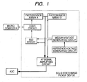
- FIG. 1 is a block diagram showing a solid state image pickup device for detecting focus according to a first embodiment of the present invention and an external control block.
- photosensor arrays are image pickup elements each for outputting an image signal of an object.
- the photosensor arrays are provided in a pair, and a distance between peak signals outputted from both of the photosensor arrays is obtained to detect focus.
- An AF signal amplifying circuit level-shifts an output from the photosensor array and applies a gain to'the level-shifted output.
- a reference voltage generating circuit generates a band gap reference voltage.
- a median voltage generating circuit generates, based on the band gap reference voltage, median voltages such as an accumulation end voltage and an output reference voltage in the solid state image pickup device.
- An auto gain control (AGC) circuit monitors a maximum output from the photosensor array and outputs an accumulation end detection signal.
- a logic circuit controls a driving of the photosensor array.
- An external microcomputer controls the solid state image pickup device, and an output from the solid state image pickup device is inputted to an external ADC.
- FIG. 2 shows an example of a circuit diagram of the AF signal amplifying circuit of FIG. 1.
- the AF signal amplifying circuit includes: an input terminal 1 to which the output from the photosensor array is inputted; a capacitor 2 for level shift; a switch 3 for level shift; an input terminal 4 at an output reference voltage; variable resistors 5 and 6 for determining an amount of gain; an operational amplifier 7; and an output terminal 8.
- the level shift means according to the present invention has a simple structure composed of a capacitor and a switch. This simple structure can reduce an area for layout.
- FIG. 3 shows a driving sequence based on the dark reference output in the AF signal amplifying circuit of FIG. 2
- FIG. 4 shows a driving sequence based on the peak reference output in the AF signal amplifying circuit of FIG. 2.
- the level shift means follows the sequence described below. First, the sequence based on the dark reference output is described. In the dark reference output, a reference voltage is set to a dark reference output voltage Vd.
- the Vd is generally set to a voltage close to a ground voltage (GND) to expand an output dynamic range.
- a reference voltage is set to a peak reference output voltage Vp.
- the Vp is generally set to a voltage close to VDD to expand an output dynamic range.
- a switch is turned on at a timing when a voltage Vpeak of peak output is inputted to the amplifier circuit input of FIG. 2.
- the image output Vn obtained from a low-contrast object is small in amplitude as shown in FIG. 9A, and average values of the Vn are distributed around the accumulation end voltage level. Accordingly, a difference between each of the average values of the Vn and Vob is large while a difference between each of the average values of the Vn and Vpeak is small.
- a large gain must be applied.
- the value of Vn-Vop with no gain applied is already so large that the gain cannot be increased as much as is sufficient.
- a signal output applied with a large gain exceeds the upper limit of output of the amplifier circuit to thereby saturate the output of the AF signal amplifying circuit.
- the operational amplifier and the variable resistors are used to form the noninverting amplifier.
- the noninverting amplifier may be replaced with an inverting amplifier.
- Vd needs to be set close to a power source voltage
- Vp needs to be set close to a ground voltage (GND).
- FIG. 5 shows the AGC circuit of FIG. 1.
- the AGC circuit includes: an input terminal 9 at output voltage of a photodiode; an operational amplifier 10; an NMOS 11 connected to a source through a drain; a constant-current power supplies 12a and 12b; and a switch 13.
- the input terminal 9, the operational amplifier 10, the NMOS 11, the constant-current power supplies 12a and 12b, and the switch 13 are provided for each pixel of the photosensor array.
- the input terminal 9, the operational amplifier 10, the NMOS 11, the constant-current power supply 12 each connected to switches 13A and 13B, respectively, are not shown in FIG. 5.
- FIG. 5 also shows an input terminal 14 at an accumulation end level, a comparator 15, and a terminal 16 for outputting an accumulation end judgment result.
- Pixel signal output and auto gain control (AGC) operation are described below.
- Output from the photodiode is inputted to the operational amplifier to drive a gate of the NMOS forming a source follower. Variations in threshold of the source follower can be corrected because the output from the source follower is fed back to the operational amplifier.
- the constant-current power supply 12b is turned on and the constant-current power supply 12b is turned off to input pixel signals to the AF signal amplifying circuit.
- the constant-current power supply 12b is turned off and the constant-current power supply 12a is turned on for the auto gain control (AGC) operation.
- the constant-current power supply 12a serves as a common power source to drive the source of the NMOS through the switch, which makes it possible to obtain a maximum voltage of each pixel as an output from the source follower. Also, AGC can be performed on all the effective pixels or on the pixels in a center portion through on and off of the switch. When the maximum voltage outputted from each of the pixels is inputted to the comparator and reaches the accumulation end voltage level, the detection signal outputted from the comparator is highlighted.
- FIG. 6 is a diagram showing an AF signal amplifying circuit according to a second embodiment of the present invention.
- FIG. 6 shows a switch 17 which operates at the same timing of the switch 3.
- the AF signal amplifying circuit according to the second embodiment can follow the operation sequence same as that of the first embodiment.
- the AF signal amplifying circuit according to the second embodiment is different from that of the first embodiment in that the switch 17 is additionally provided to obtain a unity gain outputted from the operational amplifier. A difference between the unity gain outputted from the operational amplifier and the output reference voltage is recorded to thereby eliminate a DC offset held by the operational amplifier.
- the operational amplifier and a variable resistor are used to form the noninverting amplifier.
- the noninverting amplifier may be replaced with an inverting amplifier.
- Vd needs to be set close to a power source voltage
- Vp needs to be set close to a ground voltage (GND).
- FIG. 7 a diagram showing an AF signal amplifying circuit according to a third embodiment of the present invention.
- FIG. 7 shows variable capacitors 18 and 19 for determining an amount of gain, and a switch 20 which operates at the same timing of the switch 3.
- a current flows between the output terminal of the operational amplifier and the input terminal 4. This current is driven by the operational amplifier and therefore relates to current consumption of the operational amplifier.
- resistance values of the variable resistors 5 and 6 of FIG. 2 must be raised in order to reduce the current consumption of the operational amplifier.
- a resistor element generally has a parasitic capacitance owing to a layout. Therefore, a greater resistance value increases an area for a layout, which increases the parasitic capacitance.
- variable capacitor are used to set the gain for the operational amplifier so as to prevent the current from flowing between the output terminal of the operational amplifier and the input terminal 4 to thereby reduce the current consumption.
- the AF signal amplifying circuit according to the third embodiment can follow the operation sequence same as that of the first embodiment.
- the AF signal amplifying circuit according to the third embodiment is different from that of the first embodiment in that a switch 20 is additionally provided to reset a feedback capacitance.
- the switch 20 operates at the same timing of the switch 3.
- the operational amplifier and a variable capacitor are used to form the noninverting amplifier.
- the noninverting amplifier may be replaced with an inverting amplifier.
- the Vd needs to be set close to a power source voltage
- the Vp needs to be set close to a ground voltage (GND).
- the third embodiment and the second embodiment may be used in combination. That is, it is possible to employ such a circuit structure that the variable capacitors are used to set a gain while a difference between the unity gain outputted from the operational amplifier and the output reference voltage is recorded to thereby eliminate an offset held by the operational amplifier.
- FIG. 8 is a block diagram showing an embodiment in which the solid state image pickup element is used for a lens shutter digital compact camera (image pickup device).
- FIG. 8 shows: a barrier 201 for serving as a lens protector and a main switch; a lens 202 for forming an optical image of an object on a solid state image pickup element 204; a diaphragm 203 for varying light quantity of light that has passed through the lens 202; and the solid state image pickup element 204 for capturing an image signal which corresponds to the object formed by the lens 202.
- a solid state image pickup device 205 for AE&AF has a structure in which a photometric AE sensor circuit is added to the solid state image pickup device for detecting focus explained in the first embodiment.
- the image signal processing circuit 206 processes a signal sent from the solid state image pickup element 204, and an A/D converter 207 performs analog-digital conversion on an image signal, an AE signal, and an AF signal.
- a signal processing unit 208 makes various corrections on image data outputted from the A/D converter 207 and performs data compression.
- a timing generator 209 issues various timing signals to the solid state image pickup element 204, the image signal processing circuit 206, the A/D converter 207, the signal processing unit 208, and the like.
- a unit controlling whole and arithmetic operation 210 performs various arithmetic operations and controls the whole of the camera, and a memory unit 211 temporarily stores image data.
- An I/F unit controlling recording medium 212 records on and reads out from a recording medium, and a recording medium 213 is a removable recording medium such as a semiconductor memory for recording and reading image data.
- An external I/F unit 214 is used for communicating with an external computer and the like.
- the barrier 201 is opened to turn on the main power source, subsequently a power source of a control system is turned on, and a power source of an imaging system circuit such as the A/D converter 207 is turned on.
- the unit controlling whole and arithmetic operation 210 calculates a distance to an object with a triangle focus detection method based on a signal outputted from an AF circuit block of the solid state image pickup device 205. Then, a lens extension amount for extending the lens 202 is determined, and the lens is driven to a predetermined position for focusing.
- the signal outputted from the solid state image pickup device 205 is subjected to analog-digital conversion by the A/D converter 207 to be inputted to the signal processing unit 208.
- the unit controlling whole and arithmetic operation 210 calculates an exposure based on the signal as data thus obtained to thereby control the exposure. Based on the result of the metering obtained though the calculation of the exposure, the unit controlling whole and arithmetic operation 210 adjusts the diaphragm 203 and a shutter speed.
- the solid state image pickup element 204 starts making a formal exposure.
- an image signal outputted from the solid state image pickup element 204 is subjected to analog-digital conversion by the A/D converter 207, passes though the signal processing unit 208, and is written into the memory unit 211 by the unit controlling whole and arithmetic operation 210.
- the signal stored as data in the memory unit 211 is controlled by the unit controlling whole and arithmetic operation 210 to pass through the I/F controlling recording medium 212 before being recorded on the removable recording medium 213.
- the data may pass through the external I/F unit 214 to be directly inputted to a computer or the like.
- the solid state image pickup device for detecting focus is applied not only to a digital compact camera, but also to a silver-halide film camera, and further to a pint adjuster for a liquid crystal projector and the like.
- a solid-state image pickup device wherein, in order to obtain an output of large amplitude from a low-contrast object without using a bottom detecting circuit to thereby increase a capturing rate, an accumulation end is determined when a maximum value signal in a photosensor array reaches a predetermined accumulation end level, and an amplifier circuit unit is provided for amplifying a signal, which is outputted from each of the pixels of the photosensor array, with reference to the maximum value signal of the photosensor array and for outputting the signal.
Landscapes
- Engineering & Computer Science (AREA)
- Multimedia (AREA)
- Signal Processing (AREA)
- Physics & Mathematics (AREA)
- Computer Vision & Pattern Recognition (AREA)
- General Physics & Mathematics (AREA)
- Optics & Photonics (AREA)
- Automatic Focus Adjustment (AREA)
- Studio Devices (AREA)
- Focusing (AREA)
- Transforming Light Signals Into Electric Signals (AREA)
Applications Claiming Priority (1)
| Application Number | Priority Date | Filing Date | Title |
|---|---|---|---|
| JP2005123527A JP4804027B2 (ja) | 2005-04-21 | 2005-04-21 | 焦点検出用固体撮像装置 |
Publications (2)
| Publication Number | Publication Date |
|---|---|
| EP1715677A2 true EP1715677A2 (fr) | 2006-10-25 |
| EP1715677A3 EP1715677A3 (fr) | 2011-09-14 |
Family
ID=36764676
Family Applications (1)
| Application Number | Title | Priority Date | Filing Date |
|---|---|---|---|
| EP06110771A Withdrawn EP1715677A3 (fr) | 2005-04-21 | 2006-03-07 | Capteur d'image à l'état solide et caméra |
Country Status (4)
| Country | Link |
|---|---|
| US (2) | US7692713B2 (fr) |
| EP (1) | EP1715677A3 (fr) |
| JP (1) | JP4804027B2 (fr) |
| CN (1) | CN100481892C (fr) |
Families Citing this family (20)
| Publication number | Priority date | Publication date | Assignee | Title |
|---|---|---|---|---|
| JP4804027B2 (ja) * | 2005-04-21 | 2011-10-26 | キヤノン株式会社 | 焦点検出用固体撮像装置 |
| EP1788797B1 (fr) * | 2005-11-18 | 2013-06-26 | Canon Kabushiki Kaisha | Capteur d'image à l'état solide |
| JP5110820B2 (ja) | 2006-08-02 | 2012-12-26 | キヤノン株式会社 | 光電変換装置、光電変換装置の製造方法及び撮像システム |
| JP4194633B2 (ja) * | 2006-08-08 | 2008-12-10 | キヤノン株式会社 | 撮像装置及び撮像システム |
| JP4208929B2 (ja) | 2007-02-27 | 2009-01-14 | キヤノン株式会社 | 焦点検出装置 |
| JP2009021809A (ja) * | 2007-07-11 | 2009-01-29 | Canon Inc | 撮像装置の駆動方法、撮像装置、及び撮像システム |
| JP5164531B2 (ja) | 2007-11-13 | 2013-03-21 | キヤノン株式会社 | 固体撮像装置 |
| JP5014114B2 (ja) * | 2007-12-28 | 2012-08-29 | キヤノン株式会社 | 撮像装置及び撮像システム |
| JP5111157B2 (ja) * | 2008-02-27 | 2012-12-26 | キヤノン株式会社 | 光電変換装置及び光電変換装置を用いた撮像システム |
| JP5311954B2 (ja) * | 2008-09-30 | 2013-10-09 | キヤノン株式会社 | 固体撮像装置の駆動方法 |
| JP5241454B2 (ja) * | 2008-12-01 | 2013-07-17 | キヤノン株式会社 | 固体撮像装置及びそれを用いた撮像システム |
| JP2011004390A (ja) * | 2009-05-18 | 2011-01-06 | Canon Inc | 撮像装置、撮像システム、及び撮像装置の駆動方法 |
| JP5868056B2 (ja) | 2011-07-27 | 2016-02-24 | キヤノン株式会社 | 光電変換装置、焦点検出装置及び撮像システム |
| JP5864990B2 (ja) | 2011-10-03 | 2016-02-17 | キヤノン株式会社 | 固体撮像装置およびカメラ |
| JP6108884B2 (ja) | 2013-03-08 | 2017-04-05 | キヤノン株式会社 | 光電変換装置及び撮像システム |
| JP6161454B2 (ja) | 2013-07-25 | 2017-07-12 | キヤノン株式会社 | 光電変換装置、その製造方法及びカメラ |
| US9362320B2 (en) * | 2014-06-03 | 2016-06-07 | Taiwan Semiconductor Manufacturing Company, Ltd. | Integrated circuit having a level shifter and method of making the same |
| JP7154795B2 (ja) | 2018-03-29 | 2022-10-18 | キヤノン株式会社 | 撮像装置、撮像システム、および移動体 |
| EP3861718A1 (fr) * | 2018-10-04 | 2021-08-11 | Raytheon Company | Mise a zéro automatique de pixels d'injection directe mis en tampon |
| CN111565263A (zh) * | 2019-01-29 | 2020-08-21 | 广州印芯半导体技术有限公司 | 图像传感器及其像素阵列电路 |
Citations (2)
| Publication number | Priority date | Publication date | Assignee | Title |
|---|---|---|---|---|
| US4902886A (en) * | 1989-01-23 | 1990-02-20 | Hewlett-Packard Company | Noise reduction for photodiode arrays |
| JPH04251811A (ja) | 1991-01-28 | 1992-09-08 | Canon Inc | 画像出力装置 |
Family Cites Families (21)
| Publication number | Priority date | Publication date | Assignee | Title |
|---|---|---|---|---|
| JPS6145685A (ja) | 1984-08-09 | 1986-03-05 | Canon Inc | 撮像装置 |
| JPH0672974B2 (ja) * | 1987-02-24 | 1994-09-14 | コニカ株式会社 | カメラの焦点検出装置 |
| US5182658A (en) * | 1988-07-27 | 1993-01-26 | Canon Kabushiki Kaisha | Image pickup apparatus for controlling accumulation time in photoelectric elements |
| US5900927A (en) * | 1993-10-13 | 1999-05-04 | Fuji Photo Film Co., Ltd. | Variable target autofocusing and range finder for measuring distance to a subject |
| JPH07298145A (ja) * | 1994-04-28 | 1995-11-10 | Canon Inc | 光電変換装置 |
| JPH0875995A (ja) * | 1994-09-07 | 1996-03-22 | Nikon Corp | 焦点検出装置 |
| US5617093A (en) * | 1994-09-30 | 1997-04-01 | Imp, Inc. | Switched capacitor analog circuits with low input capacitance |
| JP3808912B2 (ja) * | 1995-03-14 | 2006-08-16 | ペンタックス株式会社 | 焦点検出センサ装置 |
| US6025875A (en) * | 1995-10-23 | 2000-02-15 | National Semiconductor Corporation | Analog signal sampler for imaging systems |
| US6215961B1 (en) * | 1996-01-29 | 2001-04-10 | Minolta Co., Ltd. | Camera |
| JPH09274133A (ja) * | 1996-01-31 | 1997-10-21 | Canon Inc | 相関器と画像相関器、信号加算器、画像処理回路及びこれらを用いた自動焦点カメラ |
| US5917960A (en) | 1996-01-31 | 1999-06-29 | Canon Kabushiki Kaisha | Image correlator, an image processing apparatus using the same, and a signal adder used in the image correlator |
| US6577344B2 (en) * | 1996-09-27 | 2003-06-10 | Canon Kabushiki Kaisha | Focus state detection apparatus with image sensing device controls |
| US6035138A (en) * | 1998-01-29 | 2000-03-07 | Canon Kabushiki Kaisha | Sensor apparatus applied to distance measuring apparatus, and method for controlling sensor apparatus |
| US6973265B2 (en) * | 2001-09-27 | 2005-12-06 | Canon Kabushiki Kaisha | Solid state image pick-up device and image pick-up apparatus using such device |
| JP2003107340A (ja) * | 2001-09-27 | 2003-04-09 | Canon Inc | 測光測距用固体撮像装置及びそれを用いた撮像装置 |
| JP3754961B2 (ja) * | 2002-02-22 | 2006-03-15 | キヤノン株式会社 | 固体撮像装置およびカメラ |
| US6871018B2 (en) * | 2003-02-18 | 2005-03-22 | Pentax Corporation | Focus detection device |
| JP4804027B2 (ja) * | 2005-04-21 | 2011-10-26 | キヤノン株式会社 | 焦点検出用固体撮像装置 |
| EP1788797B1 (fr) * | 2005-11-18 | 2013-06-26 | Canon Kabushiki Kaisha | Capteur d'image à l'état solide |
| US7679422B1 (en) * | 2006-02-09 | 2010-03-16 | Cypress Semiconductor Corporation | Configurable switched capacitor block |
-
2005
- 2005-04-21 JP JP2005123527A patent/JP4804027B2/ja not_active Expired - Fee Related
-
2006
- 2006-03-07 EP EP06110771A patent/EP1715677A3/fr not_active Withdrawn
- 2006-03-16 US US11/376,204 patent/US7692713B2/en not_active Expired - Fee Related
- 2006-04-14 CN CNB2006100754220A patent/CN100481892C/zh not_active Expired - Fee Related
-
2010
- 2010-02-18 US US12/707,746 patent/US8243190B2/en not_active Expired - Fee Related
Patent Citations (2)
| Publication number | Priority date | Publication date | Assignee | Title |
|---|---|---|---|---|
| US4902886A (en) * | 1989-01-23 | 1990-02-20 | Hewlett-Packard Company | Noise reduction for photodiode arrays |
| JPH04251811A (ja) | 1991-01-28 | 1992-09-08 | Canon Inc | 画像出力装置 |
Also Published As
| Publication number | Publication date |
|---|---|
| US8243190B2 (en) | 2012-08-14 |
| CN100481892C (zh) | 2009-04-22 |
| CN1856041A (zh) | 2006-11-01 |
| US20100141818A1 (en) | 2010-06-10 |
| EP1715677A3 (fr) | 2011-09-14 |
| JP4804027B2 (ja) | 2011-10-26 |
| US7692713B2 (en) | 2010-04-06 |
| JP2006301341A (ja) | 2006-11-02 |
| US20060238633A1 (en) | 2006-10-26 |
Similar Documents
| Publication | Publication Date | Title |
|---|---|---|
| US8243190B2 (en) | Solid state image pickup device and camera with focus detection using level shifting | |
| JP4185949B2 (ja) | 光電変換装置及び撮像装置 | |
| US7394492B2 (en) | Solid state image pickup device, method of driving solid state image pickup device, and camera using the solid state image pickup device | |
| US8106955B2 (en) | Solid-state image sensing device and image sensing system | |
| US10194103B2 (en) | Solid-state imaging device and method of driving solid-state imaging device with clipping level set according to transfer operation frequency | |
| CN108702470B (zh) | 摄像元件和电子设备 | |
| US8319869B2 (en) | Solid-state imaging device | |
| EP1981260A2 (fr) | Appareil de conversion photoélectrique et système de capture d'image | |
| US20080062296A1 (en) | Photoelectric conversion device and imaging device | |
| JP2008067344A (ja) | 光電変換装置及びその制御方法並びに撮像装置 | |
| US8948584B2 (en) | Photoelectric conversion device and camera system | |
| EP1943831B1 (fr) | Capteur d'image | |
| JP2005214639A (ja) | 赤外線固体撮像素子 | |
| JP4590458B2 (ja) | 光電変換装置、撮像装置及び撮像システム | |
| JP4280446B2 (ja) | 固体撮像装置及びそれを用いた撮像装置 | |
| JP2004356866A (ja) | 撮像装置 | |
| JP4931231B2 (ja) | 撮像装置及びその制御方法 | |
| JP2010268271A (ja) | 撮像装置 | |
| JP5142680B2 (ja) | 光電変換装置及び撮像システム | |
| JPS63272185A (ja) | 焦点検出用光電変換装置 | |
| JP2008042305A (ja) | 撮像装置 | |
| JP5127467B2 (ja) | 撮像システム、及び撮像システムの制御方法 | |
| JP2001028712A (ja) | 固体撮像装置 | |
| JP2011004199A (ja) | 増幅部制御装置、及び、増幅部制御プログラム | |
| US20120033122A1 (en) | Imaging apparatus and semiconductor device |
Legal Events
| Date | Code | Title | Description |
|---|---|---|---|
| PUAI | Public reference made under article 153(3) epc to a published international application that has entered the european phase |
Free format text: ORIGINAL CODE: 0009012 |
|
| AK | Designated contracting states |
Kind code of ref document: A2 Designated state(s): AT BE BG CH CY CZ DE DK EE ES FI FR GB GR HU IE IS IT LI LT LU LV MC NL PL PT RO SE SI SK TR |
|
| AX | Request for extension of the european patent |
Extension state: AL BA HR MK YU |
|
| PUAL | Search report despatched |
Free format text: ORIGINAL CODE: 0009013 |
|
| AK | Designated contracting states |
Kind code of ref document: A3 Designated state(s): AT BE BG CH CY CZ DE DK EE ES FI FR GB GR HU IE IS IT LI LT LU LV MC NL PL PT RO SE SI SK TR |
|
| AX | Request for extension of the european patent |
Extension state: AL BA HR MK YU |
|
| RIC1 | Information provided on ipc code assigned before grant |
Ipc: H04N 5/243 20060101ALI20110808BHEP Ipc: G02B 7/34 20060101ALI20110808BHEP Ipc: H04N 5/232 20060101AFI20110808BHEP |
|
| 17P | Request for examination filed |
Effective date: 20120314 |
|
| 17Q | First examination report despatched |
Effective date: 20120404 |
|
| AKX | Designation fees paid |
Designated state(s): DE FR GB IT NL |
|
| STAA | Information on the status of an ep patent application or granted ep patent |
Free format text: STATUS: THE APPLICATION HAS BEEN WITHDRAWN |
|
| 18W | Application withdrawn |
Effective date: 20130517 |