EP1717339A2 - Appareil de depôt en continu - Google Patents
Appareil de depôt en continu Download PDFInfo
- Publication number
- EP1717339A2 EP1717339A2 EP06112340A EP06112340A EP1717339A2 EP 1717339 A2 EP1717339 A2 EP 1717339A2 EP 06112340 A EP06112340 A EP 06112340A EP 06112340 A EP06112340 A EP 06112340A EP 1717339 A2 EP1717339 A2 EP 1717339A2
- Authority
- EP
- European Patent Office
- Prior art keywords
- mask
- transport
- substrate
- coating
- stations
- Prior art date
- Legal status (The legal status is an assumption and is not a legal conclusion. Google has not performed a legal analysis and makes no representation as to the accuracy of the status listed.)
- Withdrawn
Links
- 238000000576 coating method Methods 0.000 title claims description 112
- 239000011248 coating agent Substances 0.000 title claims description 87
- 239000000758 substrate Substances 0.000 claims abstract description 229
- 239000000969 carrier Substances 0.000 claims abstract description 41
- 238000000034 method Methods 0.000 claims abstract description 27
- 239000000463 material Substances 0.000 claims abstract description 19
- 238000000151 deposition Methods 0.000 claims abstract description 12
- 230000008021 deposition Effects 0.000 claims abstract description 9
- 230000008569 process Effects 0.000 claims abstract description 9
- 238000010924 continuous production Methods 0.000 claims abstract description 4
- 238000012546 transfer Methods 0.000 claims description 39
- 238000004140 cleaning Methods 0.000 claims description 36
- 230000008859 change Effects 0.000 claims description 13
- 238000002347 injection Methods 0.000 claims description 10
- 239000007924 injection Substances 0.000 claims description 10
- 238000000678 plasma activation Methods 0.000 claims description 10
- 238000003860 storage Methods 0.000 claims description 9
- 230000000903 blocking effect Effects 0.000 claims description 7
- 238000001771 vacuum deposition Methods 0.000 claims description 7
- 230000015654 memory Effects 0.000 claims description 6
- 230000005525 hole transport Effects 0.000 claims description 4
- 238000001994 activation Methods 0.000 claims description 3
- 230000004913 activation Effects 0.000 claims description 3
- 230000007246 mechanism Effects 0.000 claims description 3
- 238000007740 vapor deposition Methods 0.000 claims description 3
- CBENFWSGALASAD-UHFFFAOYSA-N Ozone Chemical compound [O-][O+]=O CBENFWSGALASAD-UHFFFAOYSA-N 0.000 claims description 2
- 238000005229 chemical vapour deposition Methods 0.000 claims 4
- 238000005240 physical vapour deposition Methods 0.000 claims 4
- 208000028659 discharge Diseases 0.000 claims 3
- 239000012159 carrier gas Substances 0.000 claims 2
- 238000004544 sputter deposition Methods 0.000 claims 2
- 238000010884 ion-beam technique Methods 0.000 claims 1
- 238000004519 manufacturing process Methods 0.000 description 11
- 238000011109 contamination Methods 0.000 description 4
- 238000013461 design Methods 0.000 description 4
- 238000003780 insertion Methods 0.000 description 4
- 230000037431 insertion Effects 0.000 description 4
- 238000000926 separation method Methods 0.000 description 4
- 230000008901 benefit Effects 0.000 description 3
- 230000000873 masking effect Effects 0.000 description 3
- 230000015572 biosynthetic process Effects 0.000 description 2
- 238000001704 evaporation Methods 0.000 description 2
- 230000008020 evaporation Effects 0.000 description 2
- 230000006870 function Effects 0.000 description 2
- 230000001965 increasing effect Effects 0.000 description 2
- 230000001939 inductive effect Effects 0.000 description 2
- 239000000243 solution Substances 0.000 description 2
- 230000003068 static effect Effects 0.000 description 2
- 238000002207 thermal evaporation Methods 0.000 description 2
- XAGFODPZIPBFFR-UHFFFAOYSA-N aluminium Chemical compound [Al] XAGFODPZIPBFFR-UHFFFAOYSA-N 0.000 description 1
- 229910052782 aluminium Inorganic materials 0.000 description 1
- 239000000872 buffer Substances 0.000 description 1
- 230000003139 buffering effect Effects 0.000 description 1
- 238000006243 chemical reaction Methods 0.000 description 1
- 125000004122 cyclic group Chemical group 0.000 description 1
- 230000002950 deficient Effects 0.000 description 1
- 230000001419 dependent effect Effects 0.000 description 1
- 239000007772 electrode material Substances 0.000 description 1
- 238000005516 engineering process Methods 0.000 description 1
- 230000007613 environmental effect Effects 0.000 description 1
- 239000011261 inert gas Substances 0.000 description 1
- 238000009434 installation Methods 0.000 description 1
- 238000012432 intermediate storage Methods 0.000 description 1
- 238000010849 ion bombardment Methods 0.000 description 1
- 238000005457 optimization Methods 0.000 description 1
- 238000012545 processing Methods 0.000 description 1
- 238000004064 recycling Methods 0.000 description 1
- 238000007789 sealing Methods 0.000 description 1
- 238000000638 solvent extraction Methods 0.000 description 1
- 230000007704 transition Effects 0.000 description 1
- 238000009489 vacuum treatment Methods 0.000 description 1
- 238000009423 ventilation Methods 0.000 description 1
Images

Classifications
-
- H—ELECTRICITY
- H05—ELECTRIC TECHNIQUES NOT OTHERWISE PROVIDED FOR
- H05B—ELECTRIC HEATING; ELECTRIC LIGHT SOURCES NOT OTHERWISE PROVIDED FOR; CIRCUIT ARRANGEMENTS FOR ELECTRIC LIGHT SOURCES, IN GENERAL
- H05B33/00—Electroluminescent light sources
- H05B33/10—Apparatus or processes specially adapted to the manufacture of electroluminescent light sources
-
- C—CHEMISTRY; METALLURGY
- C23—COATING METALLIC MATERIAL; COATING MATERIAL WITH METALLIC MATERIAL; CHEMICAL SURFACE TREATMENT; DIFFUSION TREATMENT OF METALLIC MATERIAL; COATING BY VACUUM EVAPORATION, BY SPUTTERING, BY ION IMPLANTATION OR BY CHEMICAL VAPOUR DEPOSITION, IN GENERAL; INHIBITING CORROSION OF METALLIC MATERIAL OR INCRUSTATION IN GENERAL
- C23C—COATING METALLIC MATERIAL; COATING MATERIAL WITH METALLIC MATERIAL; SURFACE TREATMENT OF METALLIC MATERIAL BY DIFFUSION INTO THE SURFACE, BY CHEMICAL CONVERSION OR SUBSTITUTION; COATING BY VACUUM EVAPORATION, BY SPUTTERING, BY ION IMPLANTATION OR BY CHEMICAL VAPOUR DEPOSITION, IN GENERAL
- C23C14/00—Coating by vacuum evaporation, by sputtering or by ion implantation of the coating forming material
- C23C14/04—Coating on selected surface areas, e.g. using masks
- C23C14/042—Coating on selected surface areas, e.g. using masks using masks
-
- C—CHEMISTRY; METALLURGY
- C23—COATING METALLIC MATERIAL; COATING MATERIAL WITH METALLIC MATERIAL; CHEMICAL SURFACE TREATMENT; DIFFUSION TREATMENT OF METALLIC MATERIAL; COATING BY VACUUM EVAPORATION, BY SPUTTERING, BY ION IMPLANTATION OR BY CHEMICAL VAPOUR DEPOSITION, IN GENERAL; INHIBITING CORROSION OF METALLIC MATERIAL OR INCRUSTATION IN GENERAL
- C23C—COATING METALLIC MATERIAL; COATING MATERIAL WITH METALLIC MATERIAL; SURFACE TREATMENT OF METALLIC MATERIAL BY DIFFUSION INTO THE SURFACE, BY CHEMICAL CONVERSION OR SUBSTITUTION; COATING BY VACUUM EVAPORATION, BY SPUTTERING, BY ION IMPLANTATION OR BY CHEMICAL VAPOUR DEPOSITION, IN GENERAL
- C23C14/00—Coating by vacuum evaporation, by sputtering or by ion implantation of the coating forming material
- C23C14/06—Coating by vacuum evaporation, by sputtering or by ion implantation of the coating forming material characterised by the coating material
- C23C14/14—Metallic material, boron or silicon
- C23C14/20—Metallic material, boron or silicon on organic substrates
-
- C—CHEMISTRY; METALLURGY
- C23—COATING METALLIC MATERIAL; COATING MATERIAL WITH METALLIC MATERIAL; CHEMICAL SURFACE TREATMENT; DIFFUSION TREATMENT OF METALLIC MATERIAL; COATING BY VACUUM EVAPORATION, BY SPUTTERING, BY ION IMPLANTATION OR BY CHEMICAL VAPOUR DEPOSITION, IN GENERAL; INHIBITING CORROSION OF METALLIC MATERIAL OR INCRUSTATION IN GENERAL
- C23C—COATING METALLIC MATERIAL; COATING MATERIAL WITH METALLIC MATERIAL; SURFACE TREATMENT OF METALLIC MATERIAL BY DIFFUSION INTO THE SURFACE, BY CHEMICAL CONVERSION OR SUBSTITUTION; COATING BY VACUUM EVAPORATION, BY SPUTTERING, BY ION IMPLANTATION OR BY CHEMICAL VAPOUR DEPOSITION, IN GENERAL
- C23C14/00—Coating by vacuum evaporation, by sputtering or by ion implantation of the coating forming material
- C23C14/22—Coating by vacuum evaporation, by sputtering or by ion implantation of the coating forming material characterised by the process of coating
- C23C14/56—Apparatus specially adapted for continuous coating; Arrangements for maintaining the vacuum, e.g. vacuum locks
- C23C14/568—Transferring the substrates through a series of coating stations
Definitions
- the present invention relates to a device according to the preamble of claim 1 and a method for producing substrates provided with organic electroluminescent materials (OLED).
- OLED organic electroluminescent materials
- OLED displays In which organic electroluminescent materials are deposited between electrodes on a flat transparent substrate in order to generate by means of the control via the electrodes light emissions that can be used for image display ,
- JP 2003332052 A becomes an annular arrangement different Coating stations, for example, proposed for the deposition of red, green and blue emitting electroluminescent materials, wherein a separate cleaning station for the necessary for structuring the coatings masks outside the ring at a discharge station is proposed.
- a separate cleaning station for the necessary for structuring the coatings masks outside the ring at a discharge station is proposed.
- Such a system configuration requires a great deal of effort for the separate transport path for the cleaned masks to the infeed station and with regard to the separate arrangement of the cleaning stations.
- WO 03/090260 A2 describes a device for depositing multilayer coatings on substrates, wherein the substrates are passed through the coater on a substantially linear path several times to deposit the different layers.
- a device for producing organic electroluminescent light emitting devices for mass production in which the substrate to be coated is arranged on a carrier which is guided along a track arrangement through a vacuum coating system, for example, and in which the carriers with the substrate are in adjacent coating chambers can dive to perform various coating processes there.
- the cost of lowering the substrates in the individual coating chambers both in terms of time during the coating process and structurally very high.
- all processes such as substrate cleaning, mask arrangement for the structuring and cleaning of the masks and the coatings in the various chambers must be carried out one after the other.
- OLED organic electroluminescent materials
- the proposed solution is characterized in that the coating system or device is constructed according to a dual-chamber principle, i. that the entire vacuum space of the vacuum coating system is preferably divided into two parts along the longitudinal axis, wherein a first part of the vacuum space is used to transport the carriers loaded with the substrates for coating the substrates from the loading station to the unloading station by the coating machine and the other , Second part of the system for recycling and cleaning of the substrate carrier and in particular the masks necessary for structuring serves.
- This has the advantage that a very compact system with real continuous operation as a so-called in-line system can be realized, both a stockpile for carriers and masks by guiding carriers and / or masks in endless loops is largely avoided or throughput and efficiency is significantly increased.
- the double chambers may be configured as universally usable modules, so that corresponding process tools and other facilities can be arranged as needed in the corresponding double-chamber modules. This also facilitates the conversion significantly.
- such a structure allows for a continuous transport of substrates and / or masks for microstructuring the coatings in a vacuum. This avoids contamination of the carriers or masks by the environment.
- lock chambers and / or lock devices as well as closing devices between the individual chambers or chamber modules can be provided so that certain areas can be sealed off to avoid contamination or in the case of partial ventilation of the plant.
- a plurality of second endless loops are provided for the transport of masks, which serve for structuring or microstructuring of the coatings.
- the corresponding transport arrangements of the second endless loops for the mask transport are also located with a first section in the part of the vacuum space in which the substrate transport takes place from the entry area into the discharge area and with a second section for the return transport in the second part of the vacuum space.
- At least one transport branch can be provided, in which the transport device for the substrate carriers and / or the transport arrangement for the masks are not formed in the manner of a circulating loop, but in the double chambers parallel transport sections are provided in the same direction and / or opposite direction.
- This can be advantageous, in particular, in the introduction and discharge area, since in this way both parts of the vacuum double chambers can be used for transporting the substrates to the substrate carriers for the first mask application station or for a corresponding removal, thereby significantly increasing the efficiency. Accordingly, more substrates can be introduced into the coating process shortly after one another, which further increases the efficiency of the plant.
- the transport devices for the carriers and the transport arrangements for the masks partly use the same means of transport and handling devices, so that at least part of the transport takes place together.
- the substrate carriers preferably also serve as mask carriers for the at least partial return transport of the masks.
- the change from the first section of the transport device or the transport arrangement to the second section of the transport device or transport arrangements takes place in the endless loops and vice versa in the substrate loading stations and / or Substratentladestationen in which the substrates are arranged on the carriers or removed from these and / or in the mask application stations and / or mask removal stations at which the masks are assigned to the substrates or are removed therefrom or removed therefrom.
- a rotation module which performs both the mask change for two adjacent coating areas in one station as well as the transfer of the masks from the coating section into the cleaning section and vice versa, wherein on the rotation module corresponding mask application and / or removal stations and Masks and masking and holding elements for the masks are provided.
- the rotary module comprises a rotary mechanism with a Turntable on which two images are provided with transfer positions for substrate carrier both from the first section and from the second section of the transport device, wherein by rotation of the turntable by 180 °, the recordings in transfer positions of the respective other transport section and rotation by 90 ° in transfer positions for transfer into an adjacently arranged mask and / or substrate carrier change region can be brought.
- the masks are removed from the substrate carriers, then the substrate carriers are assigned to the respective other waiting mask and moved further after application in the transport system.
- mask and / or substrate carrier storage along the transport path for the substrate carrier and / or masks may be provided to replace substrate carrier and / or masks or to make at the different duration of handling processes to optimize the throughput and efficiency of the device.
- the memories can also be used for equipping the system.
- buffers which may have one or in particular a plurality of memory locations, are associated with the transfer devices, mask application and / or mask removal station and / or the rotation modules.
- Substratzin- or mask transfer units that provide appropriate rotational and / or translational movements for the respective handling options, the corresponding substrate carriers and / or masks can be easily removed from the transport process and reintroduced and also between storage units, such as several together arranged memory to be exchanged.
- mask and / or substrate carrier storage and additional mask and / or substrate carrier cleaning stations may be provided in side branches outside the actual transport path, so that by short-term removal from the actual Transport path cleaning of the masks and / or substrate support can be made. This can in particular be done in addition to the cleaning, which can take place during the return transport process in the second section or in the second part of the vacuum chamber.
- the endless loops can be realized by a single continuously operating transport device or by a plurality of handling devices and transport means, in which, for example, the substrates and / or carriers or the masks are transferred from one device to the other. Accordingly, the transport of the masks and / or substrate carriers can take place completely continuously, ie without stopping, or discontinuously with intermediate stops and / or any desired combinations thereof. A temporary return transport in individual stations is thus possible and conceivable.
- the coating or general treatment of the substrates can be done dynamically, ie during transport, or static, in which the substrate is not moved. Consequently, there are three basic possibilities for the coating or treatment types that can be combined with each other, namely continuously dynamic, cyclic dynamic or static.
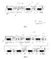
- Fig. 1 is a plan view of a device according to the invention.
- Fig. 2 is a plan view of a second embodiment of a device according to the invention.
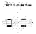
- Fig. 3 is a partial view of the device of Fig. 2 with corresponding carriers and masks;
- FIG. 4 shows a schematic representation of a part of the method sequence or operation of the device from FIGS. 2 and 3;
- Fig. 5 is a plan view of a rotary module in another embodiment of the invention.
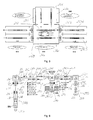
- Fig. 6 is a plan view of a third embodiment of the device according to the invention in the design for the production of white OLEDs.
- Fig. 7 is a plan view of a fourth embodiment of a device according to the invention in the design for an RGB OLED coating.
- the device 1 shows a device according to the invention with a configuration for producing white light-emitting organic LEDs (OLEDs).
- the device 1 comprises a plurality of successively arranged vacuum double chambers 2, which are each divided into two parts (halves) 3 and 4 and form a vacuum space with their adjacent chambers.
- the vacuum space is also divided by the Masêtbringungsstation 14 and the mask removal station 13 in the embodiment shown in Fig. 1 in two areas, which also have a division into several areas can.
- the subdivision by the mask application and removal stations 13 and 14 is just as little as the longitudinal division into the parts 3 and 4 to understand that there are different vacuum conditions.
- a separation can take place in that sluices or closure elements 20 are provided, which allow a separation or partitioning off of individual regions of the vacuum space.
- the vacuum space is constructed of similar modules which are differently equipped according to their use as mask application and removal stations or substrate loading and unloading stations, coating stations and the like.
- the device 1 has an overall linear structure, wherein at one end of a Substratseinschleus adopted 5 and at the opposite end a Substratausschleus driving 6 are provided. In addition to the linear structure, of course, another structure with corresponding curves or a transport around the corner is possible.
- substrate insertion device 5 and the Substratausschleus driving 6 a substrate to be coated by environmental conditions or other vacuum treatment plant in the vacuum space of the device 1 are introduced or discharged again.
- Substrate insertion device 5 is followed, after an unspecified lock or closure device, by substrate charging station 7, in which the substrate to be coated is placed on a support 40 (see FIG. 3), on which the substrate strikes during the coating process or during the transport through the device 1 is located.
- the substrate loading station 7 provides a transfer device, as shown in the partial image at the bottom right of FIG. 1, which allows a change of the carrier 40 from the part 4 of the vacuum space in the part 3 of the vacuum space and vice versa.
- the carrier 40 in the substrate loading station changes its transport direction from the Carrier return transport direction in the substrate transport direction.
- the substrate loading station can also be provided in the substrate inserting device, so that the handling of the substrate during positioning on the substrate carrier can easily take place in air and not in vacuum.
- the substrate-inserting device would only be followed by a transfer module in which the returned substrate carrier is transferred from the part 4 into the part 3 and subsequently transported into the substrate-inserting device for loading. Accordingly, the discharge area could be designed.
- the mask application station 8 follows, in which a mask (shadow mask) (see FIG. 3) is placed on or assigned to the substrate arranged in or on the carrier 40 in order to structurise the coating in the subsequent coating in that the substrate is not coated in the areas covered by the mask, while coating takes place in the other areas.
- a mask shadow mask
- the mask is aligned or adjusted here so that the structuring can be carried out in a location-specific manner.
- the mask application station 8 also comprises a transfer device, not shown, by means of which a mask can be transferred from the part 4 of the vacuum space into the part 3 of the vacuum space, wherein at the same time the mask likewise changes the transport direction from a return transport direction into a substrate transport direction.
- a transfer device not shown, by means of which a mask can be transferred from the part 4 of the vacuum space into the part 3 of the vacuum space, wherein at the same time the mask likewise changes the transport direction from a return transport direction into a substrate transport direction.
- the mask application station 8 is adjoined by a multiplicity of vacuum double chambers 2, which are equipped in or on the part 3 for corresponding coating processes.
- coating areas 9, 10 and 11 are provided, in which corresponding auxiliary layers, such as Hole injection layer HIL, hole transport layer HTL and electron blocking layer EBL in the region 9 and the light-emitting material in the region 10 and other auxiliary layers, such as electron injection layer EIL, electron transport layer ETL and hole blocking layer HBL in the region 11 are applied.
- auxiliary layers such as Hole injection layer HIL, hole transport layer HTL and electron blocking layer EBL in the region 9 and the light-emitting material in the region 10 and other auxiliary layers, such as electron injection layer EIL, electron transport layer ETL and hole blocking layer HBL in the region 11 are applied.
- the carrier After having passed through the coating regions 9 to 11 with the substrate and the mask attached thereto, the carrier passes into the adjoining mask removal station 13 where the mask is removed from the substrate.
- the mask removal station 13 also has a transfer device, by means of which the removed mask is transferred into the part 4 of the vacuum space in order to be transported back to the mask application station 8 counter to the substrate transport direction, which runs from left to right in the embodiment of FIG ,
- a mask cleaning station 12 is provided in one of the vacuum double chambers 2, which performs a cleaning of the mask and removal of the applied in the coating stations 9 to 11 coating materials directly on the return transport of the mask. In this way, the mask can be immediately used again in the mask application station 8.
- the cleaning can be done in any suitable way.
- the carrier moves with the substrate into the mask application station 14 located downstream of the mask removal station 13, in which, similar to the mask application station 8, a new mask is again applied to the substrate to provide a correspondingly adapted mask for subsequent electrode application by thermal evaporation ,
- the corresponding mask is transferred from the part 4 of the vacuum space to the part 3 of the vacuum space, the mask changing its transport direction.
- an orientation of the mask is carried out in the mask application station 14 as well as in the mask application station 8, so that the structuring of the coating material to be applied exactly in the areas where the structures are necessary.
- the vacuum double chambers 2 following the mask application station 14 are equipped in the region 15 in such a way that thermal evaporation of electrode material onto the substrate can take place.
- thermal evaporation of electrode material onto the substrate can take place.
- other vapor deposition methods are also applicable.
- the substrate on the support and the mask arranged thereon pass into the mask removal station 17, in which the mask is again removed from the substrate and transferred to the part 4 of the vacuum space, so that the mask is transported back against the substrate transport direction and can be cleaned in the cleaning station 16, to then immediately available again in the mask application station.
- the substrate is removed from the carrier and fed to the substrate discharge station 6 while the carrier is transported into the part 4 of the vacuum space and moved back to the substrate loading station 7.
- the carrier in the mask removal station 17 picks up the mask for the return transport and emits it again in the mask application station 14.
- the carrier picks up the mask of the preceding coating process in order to transport it to the mask receiving station 8.
- the exemplary embodiment of FIG. 1 there are three endless loops, namely a first endless loop for the carrier of the substrate extending from the substrate loading station 7 in part 3 of the vacuum space (upper row in the picture) via the mask application station 8 and the coating stations 9 to 11 and the Mask removal station 13 and mask receiving station 14 and the coating station 15 moves to the Substratentladestation 18, there to change its transport direction and then against the Substrattransportides turn to the Substratladestation 7 to be transported.
- there are two second endless loops with respect to the mask transport on the one hand for the mask for the coating processes in the coating stations 9 to 11 and on the other hand for the mask for the coating process in the coating station 15.
- the mask for the coating process in the coating stations 9 11 moves from the mask application station 8 via the coating stations 9 to 11 to the mask removal station 13 where the mask changes its transport direction and is transported back in the part 4 of the vacuum space via the mask cleaning station 12 to the mask application station 8.
- the other mask of the coating station coating process 15 moves from mask application station 14 in part 3 of the vacuum space via coating station 15 to mask removal station 17, where it also changes the direction of transport and is transported back in part 4 via cleaning station 16 to mask application station 14.
- endless loops related to the moving objects ie from the perspective of the carrier or the masks resulting endless loops can be formed by a variety of handling and transfer devices.
- a single continuous conveyor is provided.
- a transfer device is, for example, for the Substratlade- and Unloading stations 7 and 18 and the Maskenaufbringungs- and -ab shakingstationen 8, 13, 14 and 17, a simple rotating mechanism conceivable in which a support plate 70 is rotated about an axis 80 and rotated by 180 °, so that the support plate 70th points once with its corresponding side in the direction of the part 3 of the vacuum space and the other time after the rotation by 180 ° to part 4 of the vacuum space shows.
- the axis of rotation 80 of the pivotable support plate 70 is thus also arranged perpendicular to the image plane.
- FIG. 1 A corresponding representation is shown in the lower right part of Fig. 1, wherein the support plate 70 has a central axis 80 about which the support plate 70 is pivotable according to the double arrow, so that the substrate support 40 are rotated between the part 3 and 4 of the vacuum space can.
- FIG. 2 shows a further embodiment of a device according to the invention for the production of so-called RGB displays, in which pixels of red, blue or green emitting electroluminescent materials have to be prepared separately from each other in a structured manner. Accordingly, different maskings for the red, green and blue emitting electroluminescent materials to be deposited with corresponding mask deposition and removal stations 124, 125, 126, 127, 128, 129 must be provided. Accordingly, the coating station 121 for the red-emitting electroluminescent materials, a cleaning station 130 and, for the green coating station 122, a cleaning station 131 and the blue coating station a cleaning station 132 assigned to the corresponding masks.
- the coating stations 121, 122 and 123 together form the coating area 110 for the electroluminescent material.
- the coating regions 109 and 111 corresponding to the coating regions 9 and 11 of the embodiment of Fig. 1 are also provided in which the respective auxiliary layers such as hole-inducing layer, hole transporting layer, EBL layer, electron-inducing layer, electron-transporting layer and HBL layer be applied.
- Cleaning stations 112 and 133 are also assigned to these coating stations 109 and 111 for the masks used there.
- a plasma activation station 119 is provided at the beginning of the device 100, in which the substrate or its surface is plasma-activated for the subsequent coating.
- the device 100 is also divided into two with its vacuum space along the longitudinal axis, into the part 103 and the part 104, wherein in part 103 or correspondingly at the parts 103 of the vacuum double chambers 102 provided there, the corresponding substrate treatment and coating stations 109, 110, 111, 115 and 119 are provided, while the or the parts 104, the cleaning stations 112, 130, 131, 132, 133 and 116 are assigned or arranged on this or in this.
- corresponding closure and closing devices 120 are also provided in the embodiment of the device 100, for example between the plasma activation station 119 and the coating station 109 for separating the corresponding atmospheres and formation of a lock area are provided for the substrates.
- the device 106 has second endless loops for the respective masks, the first mask in the mask application station 108 being placed on the substrate relative to the substrate and aligned with the substrate during passage of the plasma activation station 119 and the coating station 109 in the respective areas to protect and release only previously defined areas.
- this mask is removed from the substrate or carrier and transported back to the mask application station 108 in the vacuum subspace 104, passing through the mask cleaning station 112.
- the mask deposition and alignment station 108 may also be provided between the plasma activation station 119 and the coating station 109.
- other processing techniques for cleaning and / or activation for the Surface in particular surface activation techniques conceivable, such as UV, ozone treatment or ion bombardment.
- the second endless loop of the second type for transporting a corresponding mask is provided for the coating area 121, wherein the mask is applied and adjusted in the mask application station 114 and removed from the substrate or carrier in the mask removal station 124 and cleaned in the cleaning station 130.
- the third, fourth, fifth and sixth endless loops of the second type are assigned to the coating stations 122, 123, 111 and 115, wherein the mask for the subsequent coating process is applied to the substrate or the carrier in the respective mask application stations 125, 127, 129 and 135 and are aligned, while in the arranged after the respective coating stations Maskabdgingstationen 126, 128, 134 and 117, the corresponding masks are removed again.
- FIGS. 3 and 4 This mode of operation is illustrated by the schematic representations of FIGS. 3 and 4, wherein in FIG. 3 for a partial section of the device 100 from FIG. 2 the transport or movement flow for the carrier 40 and the masks 50 and 51 or 52 is shown. As can be seen clearly in FIG. 3, both the first and the second endless loops always move simultaneously several carriers and masks, so that a high throughput is ensured by the coating system.
- the schematically illustrated first endless loop 140 and the second endless loops 150 can preferably have identical transport means and handling devices for realizing the transport device for the carrier or the transport arrangement for the masks.
- the transfer of the masks when changing from the red coating station 121 to the green coating station 122 in the mask removal station 124 and the mask receiving station 125 is schematically illustrated by, for example, rotatable support plates 70 as shown in FIG.
- the carrier with the mask is transferred from the red coating area 121 by rotation of the carrier plate 70 from the first part 103 of the vacuum space into the second part 104 of the vacuum space, in order to dispense the mask for the red coating area.
- the carrier plate 70 is then rotated back so that the carrier 40 (not shown) arranged on the carrier plate 70 with the substrate arranged thereon again lies in the region of the first part 103 of the vacuum chamber.
- a rotation module 260 with a rotation region 262 and a mask change region 261 is provided.
- the substrate carriers 266 are introduced with correspondingly coated masks, while in the part 204 the substrate carriers 267 are transferred with cleaned masks of the adjacent coating area, the transport directions being opposite.
- this is rotated by 90 °, so that the substrate support 266,267 can be transferred by linear movement in the adjacent mask exchange region 261.
- There mask masking systems 264 and 265 are arranged on the outer walls, which take over the masks of the substrate carriers 266.267.
- the substrate carriers are again moved onto the turntable 263, rotated there through 180 °, and reinserted into the mask exchange area 261. There, the substrate carrier 266 then takes over the clean mask of the subsequent coating area, while the substrate carrier 267 moves with the coated mask into the cleaning area of the other coating area after a further rotation through 90 °.
- a mask cleaning station can be connected to the side of the rotation region 262 opposite the mask change region 261, for example when using the rotation module in the insertion region.
- FIG. 6 shows a schematic representation of another Device according to the invention for the production of white, organic light emitting diodes (White OLED).
- the device 200 shown in Figure 6 in turn has a plurality of successively arranged vacuum double chambers 202, which are separated from each other only in some places by a rotary module 260 and two turning modules 275 and some shut-off 220.
- the device With the exception of the rotation module 260, which replaces the mask application and removal stations of FIG. 1, the device corresponds in its coating regions to the device of FIG. 1, so that the same final numbers have been chosen for the reference symbols for identical or comparable components.
- the device 200 of Figure 6 differs from the device 1 of Figure 1 in that different substrate insertion and withdrawal means 270, 290 are provided.
- the substrate inserter 270 has a robot 273 which transfers the substrates to the substrate carriers in a transfer module 274.
- the transfer module is designed so that the substrate carriers can be rotated therein about an axis perpendicular to the image plane and can perform linear movements, so that the substrate carriers can be taken over and transferred to the transport sections 278 and 279 of the vacuum double chambers 202.
- the peculiarity of the substrate inserter 270 is that both transport sections 278 and 279 in the vacuum double chamber 202 can serve to supply substrates to the two mask application stations 271. This means that in the parallel transport sections 278 and 279 both a rectified and an opposite transport is possible, in contrast to the antiparallel transport in the coating areas.
- substrate cleaning stations 272 are provided, which serve to clean the substrate carrier.
- the substrate inserter 270 may operate with the turn module 275 at a much higher clock frequency than the transport device in the area of the coating areas.
- the rotary module 260 Furthermore, in the region of the rotary module 260, two substrate carrier stores 281 and 282 are provided, which are connected to one another and to the rotary module 260 by a substrate carrier transfer module 283.
- This memory unit 280 thus enables intermediate buffering of the substrate carriers, in order to enable optimization of the throughput of substrates by the coating installation. There is also the possibility of replacing defective substrate carriers.
- the storage unit can serve for equipping the system with substrate carriers.
- the rotary module 260 functions as described with reference to FIG.
- the substrate discharge area 290 has, similar to the substrate slip area, a turning module 275, mask removal stations and / or latches 276 and a substrate carrier handling module 274 that interacts with a robot 273.
- the substrate transfer module 274 and the robot 273 are arranged in a so-called glove box with inert atmosphere.
- Substratausschleus conjugate- or Memory units 276 are arranged, for the substrate carrier in both directions by mobile, so that there is a quick rejection the substrates is possible.
- the transport speed in the individual areas and sections may be different in order to allow optimal use of the entire device.
- the speed in the transport branches of the substrate inserter 270 and the substrate ejector 290 may be different than the transport speeds in the coating areas 209 to 211 and 215a and 215b, respectively.
- the transport speeds in the coating areas may be different or in the sections, d. H. in one part 203 of the vacuum double chamber and the other part 204 of the vacuum double chamber.
- the transport speed in the coating part can be different from the transport speed in the area of the return transport. This allows for optimized utilization of the entire device.
- the apparatus 200 of FIG. 6 functions to feed the substrates onto the substrate carriers provided in the substrate transfer unit 274 via the robot 273. From there, the substrate carriers equipped with the substrates are transported via a lock (not shown in detail) in the transport sections 278 or 279 of the substrate inserter 270 in the direction of the mask application stations 271. There, the masks recirculated from the part 204 via the cleaning stations 212 are applied to the substrate.
- the substrate provided with the mask is introduced with the substrate carrier via the turning module 275 into the part 203 of the vacuum chamber arrangements, for example by a corresponding rotation of substrate carrier receptacles.
- a recycled substrate support with a cleaned mask may be transferred from the portion 204 to the substrate inserter 270, and then the mask is removed and intermediately stored in the mask application station 271 until the substrate carrier returns to the substrate from the substrate transfer module 274.
- the coating regions 209, 210a, 210b, 210c, and 211 here by way of example in this order, a hole injection layer, a hole transport layer, a red emitting layer, a green emitting layer, a blue emitting layer, a hole blocking layer and an electron injection layer be applied.
- the substrate with the mask disposed thereon is received in the rotation module 260, where the mask in the mask removal station 265 is removed to be transported back in the vacuum chamber portion 204, while the coated substrate in the mask application station 264 assumes a new mask is required for the subsequent coating process in the coating chambers 215a and 215b.
- a substrate carrier transfer module 283 is provided, which operates two substrate carrier stores 281 and 282. Accordingly, substrate carriers can be exchanged here.
- the substrate with the new mask is further passed through portion 203 of the vacuum chamber through the coating stations 215a and 215b where LiF evaporation followed by aluminum evaporation and deposition occurs. Thereafter, the substrates are transferred on the substrate carriers with the masks in a turning module 275 of Substratausschleus coupled 290, from where they get into the mask removal station 276 and the substrate carrier in the substrate transfer unit 274, 273 is discharged. This takes place in an inert gas atmosphere in a so-called glove box.
- FIG. 7 shows a fourth embodiment 300, in which similar or identical components again have the same final numbers as the preceding embodiments.
- the device 300 is a coating system for the production of so-called RGB-OLED systems, in which so differently colored LEDs are deposited side by side.
- This system thus essentially corresponds the plant concept of embodiment 100, with the difference that the mask application and removal stations 113 and 114 or 124, 125, 126, 127, 128, 129, as well as 130, 134 and 135 have been replaced by corresponding rotary modules 360.
- These comprise a rotation region 362, a mask exchange region 361 with mask application station 364 and mask removal or intermediate storage station 365.
- substrate carrier transfer units 383 with one or two substrate carrier stores 381, 382 are provided on the mask exchange areas 361.
- Substrate injection with the substrate sluice device 305 after transfer by the robot 373 and substrate discharge with the substrate sluice device 306 and transfer to the robot 373 is similar to the embodiment of FIG. 2. However, only transfer modules 390 or transfer modules are provided here, which merely transfer the transfer Allow substrate carrier from the part 304 in the part 303 of the vacuum chambers. Substrate application occurs in substrate inserter 305, while substrate removal occurs in substrate ejector 306.
Landscapes
- Chemical & Material Sciences (AREA)
- Engineering & Computer Science (AREA)
- Chemical Kinetics & Catalysis (AREA)
- Materials Engineering (AREA)
- Mechanical Engineering (AREA)
- Metallurgy (AREA)
- Organic Chemistry (AREA)
- Manufacturing & Machinery (AREA)
- Electroluminescent Light Sources (AREA)
- Physical Vapour Deposition (AREA)
Priority Applications (5)
| Application Number | Priority Date | Filing Date | Title |
|---|---|---|---|
| EP06112340A EP1717339A2 (fr) | 2005-04-20 | 2006-04-06 | Appareil de depôt en continu |
| TW095112732A TW200702472A (en) | 2005-04-20 | 2006-04-10 | Continuous OLED coating machine |
| US11/406,806 US20070009652A1 (en) | 2005-04-20 | 2006-04-19 | Continuous OLED coating machine |
| KR1020060035463A KR100800236B1 (ko) | 2005-04-20 | 2006-04-19 | 연속 oled 코팅 장치 |
| JP2006116398A JP2006302898A (ja) | 2005-04-20 | 2006-04-20 | Oled連続コーティングマシン |
Applications Claiming Priority (2)
| Application Number | Priority Date | Filing Date | Title |
|---|---|---|---|
| EP05008669A EP1715078A1 (fr) | 2005-04-20 | 2005-04-20 | Dispositif de revêtement en continue pour la production de OLED |
| EP06112340A EP1717339A2 (fr) | 2005-04-20 | 2006-04-06 | Appareil de depôt en continu |
Publications (1)
| Publication Number | Publication Date |
|---|---|
| EP1717339A2 true EP1717339A2 (fr) | 2006-11-02 |
Family
ID=37024932
Family Applications (1)
| Application Number | Title | Priority Date | Filing Date |
|---|---|---|---|
| EP06112340A Withdrawn EP1717339A2 (fr) | 2005-04-20 | 2006-04-06 | Appareil de depôt en continu |
Country Status (5)
| Country | Link |
|---|---|
| US (1) | US20070009652A1 (fr) |
| EP (1) | EP1717339A2 (fr) |
| JP (1) | JP2006302898A (fr) |
| KR (1) | KR100800236B1 (fr) |
| TW (1) | TW200702472A (fr) |
Cited By (7)
| Publication number | Priority date | Publication date | Assignee | Title |
|---|---|---|---|---|
| EP2085494A1 (fr) | 2008-02-01 | 2009-08-05 | Applied Materials, Inc. | Dispositif de revêtement de type double doté d'une plaque de séparation améliorée |
| EP2098609A1 (fr) | 2008-03-05 | 2009-09-09 | Applied Materials, Inc. | Appareil de refroidissement avec module de rotation |
| EP2098608A1 (fr) | 2008-03-05 | 2009-09-09 | Applied Materials, Inc. | Appareil de revêtement avec module rotatif |
| DE102011006676A1 (de) * | 2011-04-01 | 2012-10-04 | Von Ardenne Anlagentechnik Gmbh | Verfahren zur Reduzierung der Gaslast von Substratträgern bei Vakuumprozessen |
| DE102011050016A1 (de) * | 2011-04-29 | 2012-10-31 | Waldorf Technik Gmbh & Co. Kg | Vorrichtung und Verfahren zur Herstellung von beschichteten Spritzgussteilen |
| DE102011050015A1 (de) * | 2011-04-29 | 2012-10-31 | Waldorf Technik Gmbh & Co. Kg | Vorrichtung zur Herstellung von beschichteten Spritzgussteilen |
| US9353436B2 (en) | 2008-03-05 | 2016-05-31 | Applied Materials, Inc. | Coating apparatus with rotation module |
Families Citing this family (76)
| Publication number | Priority date | Publication date | Assignee | Title |
|---|---|---|---|---|
| EP1983072A1 (fr) * | 2007-04-20 | 2008-10-22 | Applied Materials, Inc. | Dispositif et procédé de traitement pour traiter un substrat |
| EP2141733A1 (fr) * | 2008-03-14 | 2010-01-06 | Intevac, Inc. | Système et procédé pour traiter des substrats avec un masque détachable |
| KR101476445B1 (ko) * | 2008-06-09 | 2014-12-24 | 엘지디스플레이 주식회사 | 유기전계발광표시장치 |
| CN101635253A (zh) * | 2008-06-14 | 2010-01-27 | 因特维克有限公司 | 利用可拆除掩模处理基板的系统和方法 |
| JPWO2009153856A1 (ja) * | 2008-06-17 | 2011-11-24 | キヤノンアネルバ株式会社 | 防着カバー付きキャリアおよび防着カバー着脱装置 |
| US9051650B2 (en) * | 2009-01-16 | 2015-06-09 | Marca Machinery, Llc | In-line metallizer assemblies and part-coating conveyor systems incorporating the same |
| US20170038658A1 (en) | 2011-09-30 | 2017-02-09 | View, Inc. | Particle removal during fabrication of electrochromic devices |
| US9007674B2 (en) | 2011-09-30 | 2015-04-14 | View, Inc. | Defect-mitigation layers in electrochromic devices |
| US9664974B2 (en) * | 2009-03-31 | 2017-05-30 | View, Inc. | Fabrication of low defectivity electrochromic devices |
| US8802200B2 (en) * | 2009-06-09 | 2014-08-12 | Samsung Display Co., Ltd. | Method and apparatus for cleaning organic deposition materials |
| US9174250B2 (en) * | 2009-06-09 | 2015-11-03 | Samsung Display Co., Ltd. | Method and apparatus for cleaning organic deposition materials |
| JP5328726B2 (ja) | 2009-08-25 | 2013-10-30 | 三星ディスプレイ株式會社 | 薄膜蒸着装置及びこれを利用した有機発光ディスプレイ装置の製造方法 |
| JP5677785B2 (ja) * | 2009-08-27 | 2015-02-25 | 三星ディスプレイ株式會社Samsung Display Co.,Ltd. | 薄膜蒸着装置及びこれを利用した有機発光表示装置の製造方法 |
| JP5611718B2 (ja) * | 2009-08-27 | 2014-10-22 | 三星ディスプレイ株式會社Samsung Display Co.,Ltd. | 薄膜蒸着装置及びこれを利用した有機発光表示装置の製造方法 |
| US8876975B2 (en) | 2009-10-19 | 2014-11-04 | Samsung Display Co., Ltd. | Thin film deposition apparatus |
| US9325007B2 (en) * | 2009-10-27 | 2016-04-26 | Applied Materials, Inc. | Shadow mask alignment and management system |
| KR101084184B1 (ko) | 2010-01-11 | 2011-11-17 | 삼성모바일디스플레이주식회사 | 박막 증착 장치 |
| US20110262625A1 (en) * | 2010-01-11 | 2011-10-27 | Hyun-Sook Park | Thin film deposition apparatus |
| KR101174875B1 (ko) | 2010-01-14 | 2012-08-17 | 삼성디스플레이 주식회사 | 박막 증착 장치, 이를 이용한 유기 발광 디스플레이 장치의 제조방법 및 이에 따라 제조된 유기 발광 디스플레이 장치 |
| KR101193186B1 (ko) | 2010-02-01 | 2012-10-19 | 삼성디스플레이 주식회사 | 박막 증착 장치, 이를 이용한 유기 발광 디스플레이 장치의 제조방법 및 이에 따라 제조된 유기 발광 디스플레이 장치 |
| KR101156441B1 (ko) | 2010-03-11 | 2012-06-18 | 삼성모바일디스플레이주식회사 | 박막 증착 장치 |
| KR101202348B1 (ko) * | 2010-04-06 | 2012-11-16 | 삼성디스플레이 주식회사 | 박막 증착 장치 및 이를 이용한 유기 발광 표시 장치의 제조 방법 |
| KR101801351B1 (ko) * | 2010-04-28 | 2017-11-27 | 삼성디스플레이 주식회사 | 박막 증착 장치, 이를 이용한 유기 발광 표시 장치의 제조 방법 및 이를 이용하여 제조된 유기 발광 표시 장치 |
| US8894458B2 (en) | 2010-04-28 | 2014-11-25 | Samsung Display Co., Ltd. | Thin film deposition apparatus, method of manufacturing organic light-emitting display device by using the apparatus, and organic light-emitting display device manufactured by using the method |
| KR101223723B1 (ko) | 2010-07-07 | 2013-01-18 | 삼성디스플레이 주식회사 | 박막 증착 장치, 이를 이용한 유기 발광 디스플레이 장치의 제조방법 및 이에 따라 제조된 유기 발광 디스플레이 장치 |
| KR101678056B1 (ko) | 2010-09-16 | 2016-11-22 | 삼성디스플레이 주식회사 | 박막 증착 장치, 이를 이용한 유기 발광 디스플레이 장치의 제조방법 및 이에 따라 제조된 유기 발광 디스플레이 장치 |
| KR101723506B1 (ko) | 2010-10-22 | 2017-04-19 | 삼성디스플레이 주식회사 | 유기층 증착 장치 및 이를 이용한 유기 발광 디스플레이 장치의 제조 방법 |
| KR101738531B1 (ko) | 2010-10-22 | 2017-05-23 | 삼성디스플레이 주식회사 | 유기 발광 디스플레이 장치의 제조 방법 및 이에 따라 제조된 유기 발광 디스플레이 장치 |
| KR20120045865A (ko) | 2010-11-01 | 2012-05-09 | 삼성모바일디스플레이주식회사 | 유기층 증착 장치 |
| KR101739012B1 (ko) * | 2010-11-22 | 2017-05-23 | 주식회사 원익아이피에스 | 기판처리시스템 |
| KR20120065789A (ko) | 2010-12-13 | 2012-06-21 | 삼성모바일디스플레이주식회사 | 유기층 증착 장치 |
| KR101760897B1 (ko) | 2011-01-12 | 2017-07-25 | 삼성디스플레이 주식회사 | 증착원 및 이를 구비하는 유기막 증착 장치 |
| US20120237682A1 (en) * | 2011-03-18 | 2012-09-20 | Applied Materials, Inc. | In-situ mask alignment for deposition tools |
| KR101923174B1 (ko) | 2011-05-11 | 2018-11-29 | 삼성디스플레이 주식회사 | 정전 척, 상기 정전 척을 포함하는 박막 증착 장치 및 이를 이용한 유기 발광 표시 장치의 제조 방법 |
| KR101852517B1 (ko) | 2011-05-25 | 2018-04-27 | 삼성디스플레이 주식회사 | 유기층 증착 장치 및 이를 이용한 유기 발광 디스플레이 장치의 제조 방법 |
| KR101840654B1 (ko) | 2011-05-25 | 2018-03-22 | 삼성디스플레이 주식회사 | 유기층 증착 장치 및 이를 이용한 유기 발광 디스플레이 장치의 제조 방법 |
| KR101857249B1 (ko) | 2011-05-27 | 2018-05-14 | 삼성디스플레이 주식회사 | 패터닝 슬릿 시트 어셈블리, 유기막 증착 장치, 유기 발광 표시장치제조 방법 및 유기 발광 표시 장치 |
| KR101826068B1 (ko) | 2011-07-04 | 2018-02-07 | 삼성디스플레이 주식회사 | 유기층 증착 장치 |
| KR20130004830A (ko) | 2011-07-04 | 2013-01-14 | 삼성디스플레이 주식회사 | 유기층 증착 장치 및 이를 이용한 유기 발광 표시 장치의 제조 방법 |
| KR101242456B1 (ko) * | 2011-07-13 | 2013-03-12 | 주식회사 선익시스템 | 셔틀을 구비한 인라인 증착 시스템 |
| KR20130069037A (ko) | 2011-12-16 | 2013-06-26 | 삼성디스플레이 주식회사 | 유기층 증착 장치, 이를 이용한 유기 발광 표시 장치의 제조 방법 및 유기 발광 표시 장치 |
| KR101576702B1 (ko) * | 2012-06-08 | 2015-12-10 | 코오롱인더스트리 주식회사 | 유리섬유시트의 수지조성물 도포장치 |
| KR101868513B1 (ko) * | 2012-06-20 | 2018-06-20 | 주식회사 원익아이피에스 | 분리 이송 장치, 이를 포함하는 반도체 제조 장치 및 인라인 시스템 |
| KR102015872B1 (ko) * | 2012-06-22 | 2019-10-22 | 삼성디스플레이 주식회사 | 유기층 증착 장치, 이를 이용한 유기 발광 디스플레이 장치의 제조 방법 및 이에 따라 제조된 유기 발광 디스플레이 장치 |
| KR101959975B1 (ko) * | 2012-07-10 | 2019-07-16 | 삼성디스플레이 주식회사 | 유기층 증착 장치, 이를 이용한 유기 발광 디스플레이 장치의 제조 방법 및 이에 따라 제조된 유기 발광 디스플레이 장치 |
| KR101958344B1 (ko) * | 2012-07-10 | 2019-03-18 | 삼성디스플레이 주식회사 | 유기층 증착 장치, 이를 이용한 유기 발광 디스플레이 장치의 제조 방법 및 이에 따라 제조된 유기 발광 디스플레이 장치 |
| KR102013315B1 (ko) * | 2012-07-10 | 2019-08-23 | 삼성디스플레이 주식회사 | 유기 발광 디스플레이 장치의 제조 방법 및 이에 따라 제조된 유기 발광 디스플레이 장치 |
| US9496524B2 (en) | 2012-07-10 | 2016-11-15 | Samsung Display Co., Ltd. | Organic layer deposition apparatus, method of manufacturing organic light-emitting display apparatus using the same, and organic light-emitting display apparatus manufactured using the method |
| KR101959974B1 (ko) | 2012-07-10 | 2019-07-16 | 삼성디스플레이 주식회사 | 유기층 증착 장치, 이를 이용한 유기 발광 디스플레이 장치의 제조 방법 및 이에 따라 제조된 유기 발광 디스플레이 장치 |
| KR20140010303A (ko) * | 2012-07-16 | 2014-01-24 | 삼성디스플레이 주식회사 | 유기층 증착 장치, 이를 이용한 유기 발광 디스플레이 장치의 제조 방법 및 이에 따라 제조된 유기 발광 디스플레이 장치 |
| KR102048051B1 (ko) * | 2012-09-04 | 2019-11-25 | 삼성디스플레이 주식회사 | 증착 환경 검사용 마스크 조립체 및 이를 포함하는 증착 설비 |
| KR102013318B1 (ko) | 2012-09-20 | 2019-08-23 | 삼성디스플레이 주식회사 | 유기층 증착 장치, 이를 이용한 유기 발광 표시 장치의 제조 방법 및 유기 발광 표시 장치 |
| KR102052069B1 (ko) * | 2012-11-09 | 2019-12-05 | 삼성디스플레이 주식회사 | 유기층 증착 장치, 이를 이용한 유기 발광 디스플레이 장치의 제조 방법 및 이에 따라 제조된 유기 발광 디스플레이 장치 |
| CN104781448B (zh) * | 2012-11-15 | 2018-04-03 | 应用材料公司 | 用于维护边缘排除屏蔽件的方法和系统 |
| JP5968770B2 (ja) * | 2012-11-30 | 2016-08-10 | 長州産業株式会社 | 真空成膜装置 |
| KR101404986B1 (ko) * | 2012-12-28 | 2014-06-11 | 주식회사 선익시스템 | 인라인 기판처리 시스템 |
| KR102081284B1 (ko) | 2013-04-18 | 2020-02-26 | 삼성디스플레이 주식회사 | 증착장치, 이를 이용한 유기발광 디스플레이 장치 제조 방법 및 유기발광 디스플레이 장치 |
| KR102075527B1 (ko) * | 2013-05-16 | 2020-02-11 | 삼성디스플레이 주식회사 | 유기층 증착 장치 및 이를 이용한 유기 발광 디스플레이 장치의 제조 방법 |
| KR102108361B1 (ko) | 2013-06-24 | 2020-05-11 | 삼성디스플레이 주식회사 | 증착률 모니터링 장치, 이를 구비하는 유기층 증착 장치, 증착률 모니터링 방법, 및 이를 이용한 유기 발광 디스플레이 장치의 제조 방법 |
| KR102162797B1 (ko) | 2013-12-23 | 2020-10-08 | 삼성디스플레이 주식회사 | 유기 발광 디스플레이 장치의 제조 방법 |
| JP6741594B2 (ja) * | 2014-02-04 | 2020-08-19 | アプライド マテリアルズ インコーポレイテッドApplied Materials,Incorporated | キャリアによって支持された基板上に一又は複数の層を堆積させるためのシステム、及び当該システムを使用する方法 |
| WO2015149848A1 (fr) * | 2014-04-02 | 2015-10-08 | Applied Materials, Inc. | Système de traitement de substrat, module de rotation à vide pour un système de traitement de substrat et procédé de fonctionnement d'un système de traitement de substrat |
| JP6937549B2 (ja) * | 2016-06-10 | 2021-09-22 | 株式会社ジャパンディスプレイ | 発光素子の製造装置 |
| US20170250379A1 (en) * | 2016-11-28 | 2017-08-31 | Applied Materials, Inc. | Evaporation source having multiple source ejection directions |
| JP6833610B2 (ja) * | 2017-05-24 | 2021-02-24 | アプライド マテリアルズ インコーポレイテッドApplied Materials,Incorporated | 有機材料用の蒸発源、有機材料用の蒸発源を有する装置、有機材料用の蒸発源を含む蒸発堆積装置を有するシステム、及び有機材料用の蒸発源を操作するための方法 |
| KR20190087996A (ko) * | 2017-09-05 | 2019-07-25 | 어플라이드 머티어리얼스, 인코포레이티드 | 마스크 디바이스를 핸들링하는 방법들, 마스크 디바이스를 교환하기 위한 장치, 마스크 교환 챔버, 및 진공 시스템 |
| CN110581055A (zh) * | 2018-05-29 | 2019-12-17 | 深圳市永盛隆科技有限公司 | 一种设备前端模块及生产线 |
| KR102663899B1 (ko) | 2018-09-28 | 2024-05-09 | 삼성디스플레이 주식회사 | 표시 패널 |
| KR20210136207A (ko) * | 2020-05-06 | 2021-11-17 | 삼성디스플레이 주식회사 | 증착 시스템 |
| CN111663104A (zh) * | 2020-06-24 | 2020-09-15 | 武汉华星光电半导体显示技术有限公司 | 蒸镀系统及蒸镀方法 |
| JP7596670B2 (ja) * | 2020-08-24 | 2024-12-10 | 東京エレクトロン株式会社 | 基板を処理する装置、及び基板を処理する方法 |
| KR102794853B1 (ko) * | 2021-12-30 | 2025-04-16 | 주식회사 선익시스템 | 인라인 증착 시스템 및 인라인 증착 시스템의 기판 얼라인 방법 |
| KR102751571B1 (ko) * | 2021-12-30 | 2025-01-09 | 주식회사 선익시스템 | 인라인 증착 시스템 및 인라인 증착 시스템의 기판 얼라인 방법 |
| JP2024000850A (ja) * | 2022-06-21 | 2024-01-09 | 株式会社ジャパンディスプレイ | 蒸着装置及び蒸着方法 |
| US20240153803A1 (en) * | 2022-11-07 | 2024-05-09 | Applied Materials, Inc. | Semiconductor process equipment |
| CN116445881A (zh) * | 2023-04-13 | 2023-07-18 | 沈阳爱科斯科技有限公司 | 连续镀膜生产线 |
Family Cites Families (7)
| Publication number | Priority date | Publication date | Assignee | Title |
|---|---|---|---|---|
| US5474611A (en) * | 1992-05-20 | 1995-12-12 | Yoichi Murayama, Shincron Co., Ltd. | Plasma vapor deposition apparatus |
| JPH10214682A (ja) * | 1997-01-30 | 1998-08-11 | Mitsubishi Chem Corp | 有機電界発光素子の製造装置及び製造方法 |
| KR100408161B1 (ko) * | 2001-03-09 | 2003-12-01 | 정광호 | 양산용 다층 박막 제작장치 |
| JP3843225B2 (ja) * | 2001-07-12 | 2006-11-08 | 日本政策投資銀行 | 有機el素子の製造装置 |
| JP2003142260A (ja) * | 2001-10-31 | 2003-05-16 | Seiko Epson Corp | 有機el素子の製造方法及び製造装置 |
| KR100434746B1 (ko) * | 2002-03-07 | 2004-06-07 | 이재선 | El막 형성장치 |
| US8808457B2 (en) * | 2002-04-15 | 2014-08-19 | Samsung Display Co., Ltd. | Apparatus for depositing a multilayer coating on discrete sheets |
-
2006
- 2006-04-06 EP EP06112340A patent/EP1717339A2/fr not_active Withdrawn
- 2006-04-10 TW TW095112732A patent/TW200702472A/zh unknown
- 2006-04-19 US US11/406,806 patent/US20070009652A1/en not_active Abandoned
- 2006-04-19 KR KR1020060035463A patent/KR100800236B1/ko not_active Expired - Fee Related
- 2006-04-20 JP JP2006116398A patent/JP2006302898A/ja not_active Withdrawn
Cited By (9)
| Publication number | Priority date | Publication date | Assignee | Title |
|---|---|---|---|---|
| EP2085494A1 (fr) | 2008-02-01 | 2009-08-05 | Applied Materials, Inc. | Dispositif de revêtement de type double doté d'une plaque de séparation améliorée |
| EP2098609A1 (fr) | 2008-03-05 | 2009-09-09 | Applied Materials, Inc. | Appareil de refroidissement avec module de rotation |
| EP2098608A1 (fr) | 2008-03-05 | 2009-09-09 | Applied Materials, Inc. | Appareil de revêtement avec module rotatif |
| WO2009109464A1 (fr) * | 2008-03-05 | 2009-09-11 | Applied Materials Inc. | Appareil de revêtement avec module de rotation |
| US9353436B2 (en) | 2008-03-05 | 2016-05-31 | Applied Materials, Inc. | Coating apparatus with rotation module |
| DE102011006676A1 (de) * | 2011-04-01 | 2012-10-04 | Von Ardenne Anlagentechnik Gmbh | Verfahren zur Reduzierung der Gaslast von Substratträgern bei Vakuumprozessen |
| DE102011050016A1 (de) * | 2011-04-29 | 2012-10-31 | Waldorf Technik Gmbh & Co. Kg | Vorrichtung und Verfahren zur Herstellung von beschichteten Spritzgussteilen |
| DE102011050015A1 (de) * | 2011-04-29 | 2012-10-31 | Waldorf Technik Gmbh & Co. Kg | Vorrichtung zur Herstellung von beschichteten Spritzgussteilen |
| EP2518102A3 (fr) * | 2011-04-29 | 2015-05-20 | Waldorf Technik GmbH & Co. KG | Dispositif et procédé destinés à la fabrication de pièces moulées d'emballage revêtues |
Also Published As
| Publication number | Publication date |
|---|---|
| KR20060110806A (ko) | 2006-10-25 |
| US20070009652A1 (en) | 2007-01-11 |
| TW200702472A (en) | 2007-01-16 |
| KR100800236B1 (ko) | 2008-02-01 |
| JP2006302898A (ja) | 2006-11-02 |
Similar Documents
| Publication | Publication Date | Title |
|---|---|---|
| KR100800236B1 (ko) | 연속 oled 코팅 장치 | |
| EP0312694B1 (fr) | Appareil suivant le principe à carrousel pour revêtir des substrats | |
| DE102011017648B4 (de) | Dünnfilm-Abscheidungsvorrichtung, Verfahren zur Herstellung einer organischen lichtemittierenden Anzeigevorrichtung unter Verwendung der Dünnfilmabscheidungsvorrichtung und durch das Verfahren hergestellte organische lichtemittierende Anzeigevorrichtung | |
| DE112009002468T5 (de) | Organische Dünnschicht-Niederschlagsvorrichtung, organische EL-Element-Herstellungsvorrichtung und organisches Dünnschicht-Niederschlagsverfahren | |
| EP0354294B1 (fr) | Appareillage de type carrousel pour le revêtement de substrats | |
| EP1715078A1 (fr) | Dispositif de revêtement en continue pour la production de OLED | |
| DE102012222673A1 (de) | Gerät zur Abscheidung organischer Schichten, Verfahren zum Fertigen von Geräten mit organischer lichtemittierender Anzeige unter Verwendung desselben und Gerät mit organischer lichtemittierender Anzeige | |
| DE102012222927A1 (de) | Gerät zur Abscheidung organischer Schichten, Verfahren zum Fertigen von Geräten mit organischer lichtemittierender Anzeige unter Verwendung desselben und unter Verwendung des Verfahrens gefertigte Geräte mit organischer lichtemittierender Anzeige | |
| DE102008049241A1 (de) | Vorrichtung zum Aufbringen jeweils eines Mehrfachdrucks auf Packmittel | |
| KR20100132517A (ko) | 회전 모듈을 갖는 코팅 장치 | |
| DE112009003614T5 (de) | Substratbearbeitungssystem | |
| DE112006001996B4 (de) | Vakuumbearbeitungsvorrichtung | |
| KR20120039944A (ko) | 기판 증착 시스템 및 증착 방법 | |
| DE19722408C1 (de) | Vorrichtung und Verfahren zum getrennten Transportieren von Substraten | |
| DE102016203435A1 (de) | Abschnitt einer Verpackungslinie für Getränkebehältnisse und Verfahren zum Umgang mit Getränkebehältnissen während ihres Transportes entlang einer Verpackungslinie | |
| US9496317B2 (en) | Method of manufacturing organic light emitting display apparatus | |
| DE112007001872T5 (de) | Abscheidungsvorrichtung, Abscheidungssystem und Abscheidungsverfahren | |
| DE102011075092B4 (de) | Verfahren zur Herstellung eines organischen lichtemittierenden Leuchtmittels | |
| DE102013223214A1 (de) | Gerät zur Abscheidung organischer Schichten und Verfahren zur Herstellung einer organischen lichtemittierenden Anzeigevorrichtung unter Verwendung des Geräts zur Abscheidung organischer Schichten | |
| DE102014107918B4 (de) | Verfahren zur Herstellung einer organischen lichtemittierenden Anzeigevorrichtung mittels einer Vorrichtung zur Abscheidung einer organischen Schicht | |
| JP2004241319A (ja) | 成膜装置 | |
| DE112007001873T5 (de) | Abscheidungsvorrichtung, Abscheidungssystem und Abscheidungsverfahren | |
| DE102013212210A1 (de) | Organische lichtemittierende Anzeigevorrichtung und Verfahren zu ihrer Herstellung | |
| US20140329349A1 (en) | Organic layer deposition apparatus, and method of manufacturing organic light-emitting display apparatus by using the same | |
| DE102005061680B3 (de) | Einrichtung und Verfahren zur gleichzeitigen Übertragung einer Mehrzahl von elektronischen Bauteilen |
Legal Events
| Date | Code | Title | Description |
|---|---|---|---|
| PUAI | Public reference made under article 153(3) epc to a published international application that has entered the european phase |
Free format text: ORIGINAL CODE: 0009012 |
|
| 17P | Request for examination filed |
Effective date: 20060505 |
|
| AK | Designated contracting states |
Kind code of ref document: A2 Designated state(s): AT BE BG CH CY CZ DE DK EE ES FI FR GB GR HU IE IS IT LI LT LU LV MC NL PL PT RO SE SI SK TR |
|
| AX | Request for extension of the european patent |
Extension state: AL BA HR MK YU |
|
| RAP1 | Party data changed (applicant data changed or rights of an application transferred) |
Owner name: APPLIED MATERIALS GMBH & CO. KG |
|
| STAA | Information on the status of an ep patent application or granted ep patent |
Free format text: STATUS: THE APPLICATION HAS BEEN WITHDRAWN |
|
| 18W | Application withdrawn |
Effective date: 20090313 |