EP1717352A2 - Appareil pour le revêtement électrolytique - Google Patents
Appareil pour le revêtement électrolytique Download PDFInfo
- Publication number
- EP1717352A2 EP1717352A2 EP06005414A EP06005414A EP1717352A2 EP 1717352 A2 EP1717352 A2 EP 1717352A2 EP 06005414 A EP06005414 A EP 06005414A EP 06005414 A EP06005414 A EP 06005414A EP 1717352 A2 EP1717352 A2 EP 1717352A2
- Authority
- EP
- European Patent Office
- Prior art keywords
- plate
- anode
- solution tank
- cathode
- electroplating
- Prior art date
- Legal status (The legal status is an assumption and is not a legal conclusion. Google has not performed a legal analysis and makes no representation as to the accuracy of the status listed.)
- Withdrawn
Links
- 238000009713 electroplating Methods 0.000 title claims abstract description 68
- 230000005611 electricity Effects 0.000 claims description 6
- 235000012431 wafers Nutrition 0.000 description 22
- 238000007789 sealing Methods 0.000 description 11
- 239000012212 insulator Substances 0.000 description 10
- 239000004020 conductor Substances 0.000 description 5
- 238000000034 method Methods 0.000 description 5
- 238000005516 engineering process Methods 0.000 description 4
- 239000011810 insulating material Substances 0.000 description 4
- UFHFLCQGNIYNRP-UHFFFAOYSA-N Hydrogen Chemical compound [H][H] UFHFLCQGNIYNRP-UHFFFAOYSA-N 0.000 description 3
- NIXOWILDQLNWCW-UHFFFAOYSA-N acrylic acid group Chemical group C(C=C)(=O)O NIXOWILDQLNWCW-UHFFFAOYSA-N 0.000 description 3
- 229910052739 hydrogen Inorganic materials 0.000 description 3
- 239000001257 hydrogen Substances 0.000 description 3
- PXHVJJICTQNCMI-UHFFFAOYSA-N Nickel Chemical compound [Ni] PXHVJJICTQNCMI-UHFFFAOYSA-N 0.000 description 2
- -1 acryl Chemical group 0.000 description 2
- 238000009434 installation Methods 0.000 description 2
- 239000011229 interlayer Substances 0.000 description 2
- 239000000463 material Substances 0.000 description 2
- 230000007246 mechanism Effects 0.000 description 2
- 239000004065 semiconductor Substances 0.000 description 2
- 239000000758 substrate Substances 0.000 description 2
- 229910000831 Steel Inorganic materials 0.000 description 1
- 239000000919 ceramic Substances 0.000 description 1
- 238000001312 dry etching Methods 0.000 description 1
- 230000005684 electric field Effects 0.000 description 1
- 239000002657 fibrous material Substances 0.000 description 1
- 239000011521 glass Substances 0.000 description 1
- 239000012774 insulation material Substances 0.000 description 1
- 230000010354 integration Effects 0.000 description 1
- 239000007769 metal material Substances 0.000 description 1
- 229910052759 nickel Inorganic materials 0.000 description 1
- 230000003647 oxidation Effects 0.000 description 1
- 238000007254 oxidation reaction Methods 0.000 description 1
- 239000011295 pitch Substances 0.000 description 1
- 239000010959 steel Substances 0.000 description 1
- 238000003756 stirring Methods 0.000 description 1
Images



Classifications
-
- C—CHEMISTRY; METALLURGY
- C25—ELECTROLYTIC OR ELECTROPHORETIC PROCESSES; APPARATUS THEREFOR
- C25D—PROCESSES FOR THE ELECTROLYTIC OR ELECTROPHORETIC PRODUCTION OF COATINGS; ELECTROFORMING; APPARATUS THEREFOR
- C25D17/00—Constructional parts, or assemblies thereof, of cells for electrolytic coating
- C25D17/10—Electrodes, e.g. composition, counter electrode
-
- C—CHEMISTRY; METALLURGY
- C25—ELECTROLYTIC OR ELECTROPHORETIC PROCESSES; APPARATUS THEREFOR
- C25D—PROCESSES FOR THE ELECTROLYTIC OR ELECTROPHORETIC PRODUCTION OF COATINGS; ELECTROFORMING; APPARATUS THEREFOR
- C25D17/00—Constructional parts, or assemblies thereof, of cells for electrolytic coating
- C25D17/008—Current shielding devices
-
- C—CHEMISTRY; METALLURGY
- C25—ELECTROLYTIC OR ELECTROPHORETIC PROCESSES; APPARATUS THEREFOR
- C25D—PROCESSES FOR THE ELECTROLYTIC OR ELECTROPHORETIC PRODUCTION OF COATINGS; ELECTROFORMING; APPARATUS THEREFOR
- C25D17/00—Constructional parts, or assemblies thereof, of cells for electrolytic coating
- C25D17/001—Apparatus specially adapted for electrolytic coating of wafers, e.g. semiconductors or solar cells
-
- C—CHEMISTRY; METALLURGY
- C25—ELECTROLYTIC OR ELECTROPHORETIC PROCESSES; APPARATUS THEREFOR
- C25D—PROCESSES FOR THE ELECTROLYTIC OR ELECTROPHORETIC PRODUCTION OF COATINGS; ELECTROFORMING; APPARATUS THEREFOR
- C25D17/00—Constructional parts, or assemblies thereof, of cells for electrolytic coating
- C25D17/06—Suspending or supporting devices for articles to be coated
-
- C—CHEMISTRY; METALLURGY
- C25—ELECTROLYTIC OR ELECTROPHORETIC PROCESSES; APPARATUS THEREFOR
- C25D—PROCESSES FOR THE ELECTROLYTIC OR ELECTROPHORETIC PRODUCTION OF COATINGS; ELECTROFORMING; APPARATUS THEREFOR
- C25D17/00—Constructional parts, or assemblies thereof, of cells for electrolytic coating
- C25D17/10—Electrodes, e.g. composition, counter electrode
- C25D17/12—Shape or form
-
- C—CHEMISTRY; METALLURGY
- C25—ELECTROLYTIC OR ELECTROPHORETIC PROCESSES; APPARATUS THEREFOR
- C25D—PROCESSES FOR THE ELECTROLYTIC OR ELECTROPHORETIC PRODUCTION OF COATINGS; ELECTROFORMING; APPARATUS THEREFOR
- C25D7/00—Electroplating characterised by the article coated
- C25D7/12—Semiconductors
- C25D7/123—Semiconductors first coated with a seed layer or a conductive layer
Definitions
- the present invention relates to an electroplating apparatus for performing electroplating and anodic oxidation on surfaces of, for example, wafers, glass substrates, and ceramic substrates.
- wiring pitches are required to be reduced to accomplish high integration and performance.
- an interlayer insulated film is formed, and then dry etching process is performed on the interlayer insulated film to form wiring grooves into which wiring material is electroplated and filled.
- a cathode plate which is the object to be electroplated, and an anode plate are placed to face each other in a solution tank inside which electroplating solution is poured.
- a power source is connected to the cathode plate and the anode plate in order to generate electric field between the cathode plate and the anode plate to electroplate a surface of the cathode plate.
- an electroplating apparatus is rotated by 90 degrees after a cathode plate and an anode plate are installed vertically. Then, the cathode plate in a lower position and the anode plate in a higher position are held horizontally to prevent bubbles from going directly along the surface of the cathode plate.
- a method requires another device to rotate the electroplating apparatus. Accordingly, there is a problem that the whole electroplating apparatus becomes large and complicated.
- an object of the present invention to provide an electroplating apparatus which is able to form an electroplating film with an even thickness all over a surface to be electroplated so as to improve quality of the electroplating film, as well as to downsize and simplify the whole electroplating apparatus.
- an electroplating apparatus including a solution tank which has at least a bottom plate and a side plate, and inside which electroplating solution is poured, and a cathode plate and an anode plate which are horizontally placed so as to face each other in the electroplating solution in the solution tank.
- a solution tank which has at least a bottom plate and a side plate, and inside which electroplating solution is poured, and a cathode plate and an anode plate which are horizontally placed so as to face each other in the electroplating solution in the solution tank.
- one plate of the cathode plate and the anode plate is an object to be electroplated and placed in a lower position than the other plate.
- an opening through which the cathode plate and the anode plate are inserted into the solution tank is provided in the side plate of the solution tank.
- a shield plate which is detachable shields the opening of the solution tank.
- the cathode plate and the anode plate are installed, the cathode plate and the anode plate are inserted into the solution tank through the opening provided in the side plate of the solution tank. Accordingly, it is easy to install the cathode plate and the anode plate horizontally and parallel each other in the solution tank.
- the one plate of the cathode plate and the anode plate which is an object to be electroplated, is placed in the lower position than the other plate. Therefore, it is possible to let bubbles which are mainly composed of hydrogen and generated from a surface to be electroplated of the one plate, go up directly to outside without going along the surface to be electroplated of the one plate.
- the object to be electroplated may be connected to a negative electrode of a power source in order that the surface of the object to be electroplated is electroplated.
- the object to be electroplated may be also connected to a positive electrode of the power source in order that an anodic film, which is an oxide film, is formed on the surface of the object to be electroplated.
- a slot which holds the cathode plate and/or the anode plate horizontally may be provided in the side plate of the solution tank.
- a plurality of the slots which hold the cathode plate and/or the anode plate horizontally may be vertically arranged in the side plate of the solution tank in order to adjust a height of the cathode plate and/or the anode plate.
- the slots may be used to adjust a height of the other plate.
- a conductive member which conducts electricity to the other plate may be inserted downward from above toward inside of the solution tank into the other plate so as to be electrically connected to the other plate.
- the conductive member may be supported in the solution tank in such a manner that a height of the conductive member is adjustable corresponding to the height of the other plate.
- the conductive member is inserted downward from above toward inside of the solution tank.
- an end of the conductive member can be electrically connected to the other plate, which is placed in the higher of two positions of the cathode plate and the anode plate.
- the height of the conductive member in the higher position is changed, the height of the conductive member is adjusted corresponding to the height of the other plate in the higher position. Consequently, it is easy to engage and electrically connect the conductive member to the other plate in the higher position.
- the one plate may be cantilevered and attached to the shield plate.
- the one plate is attached to the shield plate in advance and then installed in the solution tank. Accordingly, the one plate can be easily cantilevered and attached to the shield plate. Thus, a worker does not need to bother to extend his/her hand into the opening of the solution tank to install the one plate in the lower position. Moreover, to install the shield plate to the solution tank, only one edge of the one plate in the lower position needs to be cantilevered.
- the other edge of the one plate in the lower position can be, for example, hung on a portion of the solution tank which faces the shield plate or engaged in a slot formed in the solution tank so that both sides of the one plate can be supported. Therefore, the one plate in the lower position is stably held in the solution tank.
- a bolt having a head may be attached to the lower side of the other end of the one plate in the lower position in order to support the other end of the one plate with the head of the bolt being touched on the bottom of the solution tank.
- a conductive member which conducts electricity to the one plate may pass through the shield plate horizontally toward inside of the solution tank so as to be electrically connected to the one plate.
- the conductive member passes through the shield plate horizontally toward inside of the solution tank. Therefore, it is easy to electrically connect the conductive member to the one plate, which is placed in the lower of two positions of the cathode plate and the anode plate.
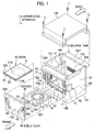
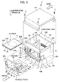
- an electroplating apparatus 1 generally includes a solution tank 10, an anode 20, a cathode 30, and a shield plate 40. Electroplating solution is poured and filled inside the solution tank 10.
- the solution tank 10 has a bottom plate 10A, a first side plate 10B as a front plate (hereafter referred as a side plate 10B), a second side plate 10C as a back plate (hereafter referred as a side plate 10C), a third side plate 10D as a left side plate (hereafter referred as a side plate 10D), a fourth side plate 10E as a right side plate (hereafter referred as a side plate 10E), and a top plate 10F which is fastened to brackets 10B1 and 10C1 respectively provided on upper ends of the side plates 10B and 10C, with bolts 11, 11, 11, and 11 (see FIG. 2). Additionally, as shown in FIG.
- a right vertical plate 14 (hereafter referred as a vertical plate 14) erected on the bottom plate 10A, a horizontal plate 13 extending horizontally from a lower portion of the vertical plate 14, and a left vertical plate 12 (hereafter referred as a vertical plate 12) erected on a left end of the horizontal plate 13 are formed inside the solution tank 10.
- a plurality of circulation holes 14A, 14A, ..., and 14A are cut through the vertical plate 14.
- a plurality of circulation holes 13A, 13A, ..., and 13A are also cut through the horizontal plate 13.
- a drain hole 10A1 is cut through the bottom plate 10A.
- a pump attachment opening 15 to which a pump (not shown) is to be attached is cut through the side plate 10C of the solution tank 10 between the side plate 10E and the vertical plate 14.
- a cover plate 16 shown in FIG. 5 is placed between upper ends of the vertical plate 12 and the vertical plate 14.
- electroplating solution is poured from the pump in direction indicated by an arrow A as shown in FIG. 3.
- the poured electroplating solution circulates in direction indicated by an arrow B through circulation holes 14A and in direction indicated by an arrow B' over the top of the vertical plate 14, so as to be poured into a space surrounded by the vertical plates 12 and 14 and the horizontal plate 13.
- the electroplating solution poured into the space circulates in direction indicated by an arrow C through circulation holes 13A and in direction indicated by an arrow D over the top of the vertical plate 12, so as to be poured under the horizontal plate 13.
- the electroplating solution is drained outside in direction indicated by an arrow F through the drain hole 10A1.
- the pump circulates the electroplating solution in predetermined direction in order to prevent the electroplating solution from staying.
- the pump prevents "residues" which are generated while a wafer (a cathode plate) 31, which will be described later, is being electroplated, from sticking on the wafer 31.
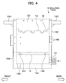
- an opening 17 is formed in a substantially two-tiered shape in the side plate 10B of the solution tank 10. Additionally, the opening 17 includes a narrow portion 17A which is horizontally narrower and a wide portion 17B which is horizontally wider and connected to a lower side of the narrow portion 17A. Moreover, a plurality of slots 18A, 18A, ..., and 18A are vertically arranged along right and left peripheries of the narrow portion 17A of the opening 17.
- the slots are formed in substantially U-shapes, and a pair of the slots face each other on the right and left peripheries.
- a plurality of slots 18B, 18B, ..., and 18B which extend and elongate in horizontal direction are formed in the side plate 10C of the solution tank 10 at positions respectively corresponding to the pairs of the slots 18A, 18A, ..., and 18A in the side plate 10B.
- a sealing member 19 formed as a substantially quadrangular frame is attached to the side plate 10B of the solution tank 10 so as to surround the periphery of the opening 17.
- holding members 51 and 51 which form parts of lock mechanisms 50 and 50 respectively are fixed and attached to a corner between the side plate 10B and the side plate 10D and a corner between the side plate 10B and the side plate 10E.
- the anode 20 includes an anode cartridge pan 21 which is made of insulation material such as acrylic and formed in a quadrangular shape having a quadrangular recess 21A, an anode plate 22 which is made of metallic material such as steel and nickel and formed in a quadrangular shape so as to fit in the recess 21 A of the anode cartridge pan 21, an anode cartridge holder 23 which is made of insulating material such as acrylic in order to hold the anode plate 22 between the anode cartridge holder 23 and the anode cartridge pans 21, an anode bag 24 which is made of fibrous material such as cloths and lined on a surface (a lower side in FIG.
- anode bag holder 25 which is made of insulating material such as acrylic to hold the anode bag 24 between the anode bag holder 25 and the anode cartridge holder 23.
- first engaging protrusions 23A and 23A formed in substantially quadrangular shapes are protruded on both sides of the front end of the anode cartridge holder 23.
- a back end of the anode cartridge holder 23 is a second engaging protrusion 23B which is protruded backward through between the anode cartridge pan 21 and the anode bag holder 25.
- the first engaging protrusions 23A and 23A are engaged in the pair of the slots 18A and 18A (See FIG. 5) while the second engaging protrusion 23B (see FIG. 8) is engaged in the slot 18B.
- the anode 20 is installed.
- the anode 20 is horizontally and stably held by three points support in the electroplating solution in the solution tank 10.
- the anode bag 24 prevents "residue", which is generated while the wafer 31 is being electroplated, from adhering to the anode plate 22.
- a conductive rod (a conductive member) 26 on an anode side is inserted from above into a circular hole 21B which is cut through the anode cartridge pan 21. Accordingly, an end (a lower end) of the conductive rod 26 on the anode side electrically contacts with the anode plate 22. Then, the conductive rod 26 on the anode side is screwed into a screw hole (not shown) which is cut through the cover plate 16. Thus, a worker can rotate the conductive rod 26 on the anode side in order to adjust the height of the end of the conductive rod 26 on the anode side corresponding to the height of the anode 20.
- a cathode 30 is substantially similar to the cathode cartridge described in JP 2003-301299A .
- the cathode 30 is placed horizontally and parallel to the anode 20 in a lower position than the anode 20.
- the cathode 30 includes the wafer 31, which is an object to be electroplated, a cathode conductor 32 which is a conductive member to conduct electricity to the surface 31A of the wafer 31, a first insulator 33 which is made of insulating material such as acryl to cover the frontside (the side of the surface 31A) of the wafer 31 and hold the cathode conductor 32, and a second insulator 34 which is made of insulating material such as acryl to cover the backside (the opposite side of the surface 31A) of the wafer 31 and hold the wafer 31.
- the cathode conductor 32 includes a conductive ring plate 32A and a conductive rod 32B on the cathode side which is electrically connected to the conductive ring
- a front edge of the first insulator 33 of the cathode 30 is fastened and attached to a shield plate 40, which will be described later, in the manner of a cantilever.
- the conductive rod 32B of the cathode conductor 32 passes through the shield plate 40 horizontally toward inside of the solution tank 10 to be electrically connected to the wafer 31 through the conductive ring plate 32A.
- insert holes 33A and 40A through which the conductive rod 32B is inserted are respectively provided in the first insulator 33 and the shield plate 40.
- the conductive rod 32B protrudes outside from the shield plate 40 through the insert holes 33A and 40A.
- a cylindrical sealing member 70 see FIG.
- the shield plate 40 which is formed as a substantially quadrangular board member, is affixed to an outer periphery of the sealing member 19 to shield the opening 17.
- a lever member 52 which forms a part of the lock mechanism 50 is provided on each of the right and left sides of the shield plate 40 so as to be rotatable. Then, an end of the lever member 52 is latched to the holding member 51 so as to strongly press the shield plate 40 toward the sealing member 19. Accordingly, it is possible to fluid-tightly seal the opening 17 with the shield plate 40 and prevent the electroplating solution from leaking from the opening 17.
- the number "60" in FIG. 5 shows a mixing tool which is able to move back and forth on the upper end of the solution tank 10.
- the mixing tool 60 generally includes a support plate 62 which has rotatable rollers 61 and 61 on front and rear sides, vertical panels 63 and 63 which vertically hang down from the support plate 62, and a connecting rod 64 which connects the lower ends of the vertical panels 63 and 63.
- an operation plate 65 which is operated from outside to move the mixing tool 60 back and forth is provided to the support plate 62.
- an actuator (not shown) actuates the operation plate 65 to move back and forth so as to cause the vertical panels 63 and 63 and the connecting rod 64 to stir the electroplating solution in order to prevent the electroplating solution from staying in the solution tank 10.
- the conductive rod 26 on the anode side is connected to a positive electrode of a power source.
- the conductive rod 32B on the cathode side is connected to a negative electrode of the power source. Accordingly, an electroplating film is formed on the surface 31A of the wafer 31 of the cathode 30.
- the cathode 30 in a lower position is placed horizontally and parallel to the anode 20 in a higher position. Therefore, it is possible to let bubbles which are mainly composed of hydrogen and generated from the surface 31A of the wafer 31 of the cathode 30, go up from the surface 31A of the wafer 31 to escape outside. Thus, the bubbles do not go along the surface 31A of the wafer 31. As a result, it is possible to equalize the thickness of the electroplating film formed on all over the surface to be electroplated to improve quality of the electroplating film.
- the opening 17 through which the anode 20 and the cathode 30 are inserted into the solution tank 10 is formed in the side plate 10B of the solution tank 10. Accordingly, it is easy to insert the anode 20 and the cathode 30 horizontally into the solution tank 10 through the opening 17.
- a large scale device which rotates the entire solution tank by 90 degrees as described in the well-known method is not necessary. As a result, it is possible to downsize and simplify the whole electroplating apparatus.
- the slots 18A are provided in the side plate 10B of the solution tank 10.
- the slot 18B is provided in the side plate 10C of the solution tank 10 at a height corresponding to the slots 18A. Accordingly, the anode 20 is engaged in the slots 18A and 18B so as to be held horizontally in the solution tank 10. Thus, it is easy to install the anode 20.
- the plurality of slots 18A, 18A, ..., and 18A and the plurality of slots 18B, 18B, ..., and 18B are respectively arranged in the side plate 10B and the side plate 10C of the solution tank 10 in vertical direction. Therefore, it is possible to change the installation position of the anode 20 corresponding to the height of the slot 18A and 18B in order to change a distance between the anode 20 and the cathode 30. As a result, it is possible to appropriately control the thickness of the electroplating film formed on the surface 31A of the wafer 31 of the cathode 30.
- the conductive rod 26 is inserted downward from above toward inside of the solution tank 10 into the anode 20 which is placed in the higher of two positions of the anode 20 and the cathode 30, so as to be electrically connected to the anode 20.
- the conductive rod 26 is supported in the solution tank 10 in such a way that the height of the conductive rod 26 can be adjusted corresponding to the height of the anode 20. Therefore, it is easy to adjust the height of the conductive rod 26 depending on the height of the anode 20 in order to engage the conductive rod 26 in the anode plate 22.
- the cathode 30 is cantilevered and attached to the shield plate 40. Therefore, to install the cathode 30, the shield plate 40 to which the cathode 30 has been attached in advance, is installed into the solution tank 10. Thus, the worker does not need to bother to extend his/her hand into the opening 17 of the solution tank 10 to install the cathode 30. As a result, it is possible to easily install the cathode 30.
- the conductive rod 32B of the cathode conductor 32 passes through the shield plate 40 horizontally so as to be electrically connected to the cathode 30 which is placed in the lower of two positions of the anode 20 and the cathode 30. Therefore, it is easy to electrically connect the conductive rod 32B to the wafer 31 of the cathode 30 through the conductive ring plate 32A.
- anode 20 is installed in the solution tank 10 in such a way that the height of the anode 20 can be changed and the cathode 30 is attached to the shield plate 40.
- the present invention is not limited to this.
- the anode 20 may be attached to the shield plate 40, and the cathode 30 may be installed in the solution tank 10 in such a way that the height of the cathode 30 can be changed.
- an anode plate may be an object to be electroplated and placed in a lower position than a cathode plate.
- an anodic film which is an oxide film, may be formed on a surface of the anode plate.
- the sealing member 70 also has a function to prevent a problem that the electroplating solution infiltrates into a portion other than the surface 31A of the wafer 31 in combination with the ring sealing members.
- the connecting rod 64 of the mixing tool 60 is formed as a round rod.
- the present invention is not limited to this.
- the cross section of the connecting rod 64 of the mixing tool 60 may be formed in a quadrangle, a triangle, or other shape.
- a thickness of an electroplating film formed on a surface to be electroplated of an object to be electroplated can be equalized all over the surface so as to improve quality of the electroplating film.
- a large scale device which rotates the solution tank by 90 degrees is not required. As a result, a whole electroplating apparatus is possible to be downsized and simplified.
Landscapes
- Chemical & Material Sciences (AREA)
- Engineering & Computer Science (AREA)
- Chemical Kinetics & Catalysis (AREA)
- Electrochemistry (AREA)
- Materials Engineering (AREA)
- Metallurgy (AREA)
- Organic Chemistry (AREA)
- Life Sciences & Earth Sciences (AREA)
- Sustainable Development (AREA)
- Electroplating Methods And Accessories (AREA)
Applications Claiming Priority (1)
| Application Number | Priority Date | Filing Date | Title |
|---|---|---|---|
| JP2005125538A JP2006299367A (ja) | 2005-04-22 | 2005-04-22 | 電気めっき試験器 |
Publications (2)
| Publication Number | Publication Date |
|---|---|
| EP1717352A2 true EP1717352A2 (fr) | 2006-11-02 |
| EP1717352A3 EP1717352A3 (fr) | 2007-01-17 |
Family
ID=36809576
Family Applications (1)
| Application Number | Title | Priority Date | Filing Date |
|---|---|---|---|
| EP06005414A Withdrawn EP1717352A3 (fr) | 2005-04-22 | 2006-03-16 | Appareil pour le revêtement électrolytique |
Country Status (6)
| Country | Link |
|---|---|
| US (1) | US20060237304A1 (fr) |
| EP (1) | EP1717352A3 (fr) |
| JP (1) | JP2006299367A (fr) |
| KR (1) | KR20060111385A (fr) |
| CN (1) | CN1865519B (fr) |
| TW (1) | TW200637935A (fr) |
Cited By (1)
| Publication number | Priority date | Publication date | Assignee | Title |
|---|---|---|---|---|
| WO2010086111A3 (fr) * | 2009-01-27 | 2010-10-07 | Fraunhofer-Gesellschaft zur Förderung der angewandten Forschung e.V. | Procédé de production de structures superficielles métallico-cristallines lors d'un dépôt électrolytique |
Families Citing this family (6)
| Publication number | Priority date | Publication date | Assignee | Title |
|---|---|---|---|---|
| EP2246460A1 (fr) * | 2009-04-28 | 2010-11-03 | Golden Eagle Trading Ltd | Installation de traitement de surface de pièces |
| JP6226229B2 (ja) * | 2013-08-19 | 2017-11-08 | 株式会社山本鍍金試験器 | めっき装置及びこれを用いたセンサ装置 |
| WO2019175990A1 (fr) * | 2018-03-13 | 2019-09-19 | 株式会社山本鍍金試験器 | Dispositif de placage et système de placage |
| CN110565154B (zh) * | 2019-09-06 | 2024-07-09 | 陕西汉和新材料科技有限公司 | 一种新型铜箔防氧化电镀阳极板 |
| JP7316908B2 (ja) * | 2019-10-30 | 2023-07-28 | 株式会社荏原製作所 | アノード組立体 |
| CN112853445B (zh) * | 2021-01-08 | 2022-08-26 | 上海戴丰科技有限公司 | 一种阳极可侧向抽拉式晶圆水平电镀池及晶圆水平电镀装置 |
Citations (1)
| Publication number | Priority date | Publication date | Assignee | Title |
|---|---|---|---|---|
| JP2003301299A (ja) | 2002-04-12 | 2003-10-24 | Yamamoto Mekki Shikenki:Kk | 電気めっき試験器の陰極カートリッジ |
Family Cites Families (14)
| Publication number | Priority date | Publication date | Assignee | Title |
|---|---|---|---|---|
| SE7603626L (sv) * | 1975-03-27 | 1977-01-04 | Otto Alfred Becker | Anordning for att galvanisera metallytor, serskilt vid snittkantytor hos genom stapling tillskurna platar |
| US4129494A (en) * | 1977-05-04 | 1978-12-12 | Norman Telfer E | Electrolytic cell for electrowinning of metals |
| US4459194A (en) * | 1983-03-10 | 1984-07-10 | At&T Technologies, Inc. | Electroplating apparatus |
| US5039381A (en) * | 1989-05-25 | 1991-08-13 | Mullarkey Edward J | Method of electroplating a precious metal on a semiconductor device, integrated circuit or the like |
| US5242563A (en) * | 1992-03-12 | 1993-09-07 | The United States Of America As Represented By The Secretary Of The Navy | Molten salt reactor for potentiostatic electroplating |
| US5312532A (en) * | 1993-01-15 | 1994-05-17 | International Business Machines Corporation | Multi-compartment eletroplating system |
| DE19729893C2 (de) * | 1997-07-12 | 1999-04-29 | Mc Micro Compact Car Ag | Lenksäule in einem Kraftfahrzeug |
| US6017437A (en) * | 1997-08-22 | 2000-01-25 | Cutek Research, Inc. | Process chamber and method for depositing and/or removing material on a substrate |
| US6416647B1 (en) * | 1998-04-21 | 2002-07-09 | Applied Materials, Inc. | Electro-chemical deposition cell for face-up processing of single semiconductor substrates |
| US6143146A (en) * | 1998-08-25 | 2000-11-07 | Strom; Doug | Filter system |
| US6217727B1 (en) * | 1999-08-30 | 2001-04-17 | Micron Technology, Inc. | Electroplating apparatus and method |
| US6627052B2 (en) * | 2000-12-12 | 2003-09-30 | International Business Machines Corporation | Electroplating apparatus with vertical electrical contact |
| JP3827627B2 (ja) * | 2002-08-13 | 2006-09-27 | 株式会社荏原製作所 | めっき装置及びめっき方法 |
| US20050189228A1 (en) * | 2004-02-27 | 2005-09-01 | Taiwan Semiconductor Manufacturing Co., Ltd. | Electroplating apparatus |
-
2005
- 2005-04-22 JP JP2005125538A patent/JP2006299367A/ja active Pending
-
2006
- 2006-03-16 EP EP06005414A patent/EP1717352A3/fr not_active Withdrawn
- 2006-03-16 TW TW095108977A patent/TW200637935A/zh unknown
- 2006-03-17 US US11/377,415 patent/US20060237304A1/en not_active Abandoned
- 2006-04-19 KR KR1020060035497A patent/KR20060111385A/ko not_active Ceased
- 2006-04-21 CN CN2006100745166A patent/CN1865519B/zh not_active Expired - Lifetime
Patent Citations (1)
| Publication number | Priority date | Publication date | Assignee | Title |
|---|---|---|---|---|
| JP2003301299A (ja) | 2002-04-12 | 2003-10-24 | Yamamoto Mekki Shikenki:Kk | 電気めっき試験器の陰極カートリッジ |
Cited By (1)
| Publication number | Priority date | Publication date | Assignee | Title |
|---|---|---|---|---|
| WO2010086111A3 (fr) * | 2009-01-27 | 2010-10-07 | Fraunhofer-Gesellschaft zur Förderung der angewandten Forschung e.V. | Procédé de production de structures superficielles métallico-cristallines lors d'un dépôt électrolytique |
Also Published As
| Publication number | Publication date |
|---|---|
| JP2006299367A (ja) | 2006-11-02 |
| TW200637935A (en) | 2006-11-01 |
| US20060237304A1 (en) | 2006-10-26 |
| KR20060111385A (ko) | 2006-10-27 |
| CN1865519B (zh) | 2010-08-11 |
| EP1717352A3 (fr) | 2007-01-17 |
| CN1865519A (zh) | 2006-11-22 |
Similar Documents
| Publication | Publication Date | Title |
|---|---|---|
| EP0606610B1 (fr) | Système de dépÔt électrolytique à plusieurs compartiments | |
| CN210176983U (zh) | 电镀设备 | |
| EP1717352A2 (fr) | Appareil pour le revêtement électrolytique | |
| US9920448B2 (en) | Inert anode electroplating processor and replenisher with anionic membranes | |
| CN1831209B (zh) | 电镀装置 | |
| JP2019014955A (ja) | レギュレーションプレート、アノードホルダ、及び基板ホルダ | |
| TWI681080B (zh) | 鍍覆裝置 | |
| KR20210010397A (ko) | 전기 화학 증착 시스템 | |
| KR102890634B1 (ko) | 기판 홀더 및 그것을 구비한 기판 도금 장치, 그리고 전기 접점 | |
| EP1438446B1 (fr) | Systeme et procede de placage electrolytique | |
| KR20040108578A (ko) | 액체 탱크 | |
| KR102898833B1 (ko) | 애노드 조립체 | |
| KR20190056460A (ko) | 인쇄회로기판의 도금편차 개선을 위한 지그장치 | |
| CN111699285B (zh) | 电解研磨用电极框架及包括其的电解研磨装置 | |
| JPWO2017037757A1 (ja) | 表面処理装置 | |
| KR101415680B1 (ko) | 전해도금장치용 차폐박스 및 전해도금장치용 전극판 | |
| KR20190064659A (ko) | 동축 전해 셀들을 위한 전극 지지 구조체 | |
| JP4424486B2 (ja) | カソード電極組立体、カソード電極装置、及び、メッキ装置 | |
| JP2022122494A (ja) | 陽極化成装置及び陽極化成方法 | |
| CN222182492U (zh) | 一种水平旋转晶圆电镀设备和晶圆电镀装置 | |
| CN222557118U (zh) | 一种电镀载具及电镀设备 | |
| CN117344364A (zh) | 电镀装置及晶圆的电镀方法 | |
| CN214177657U (zh) | 一种pcb板加工固定装置 | |
| JP2006328470A (ja) | 電気めっき装置 | |
| WO2025227581A1 (fr) | Appareil d'électroplacage, dispositif d'électroplacage, appareil d'anode d'électroplacage et appareil d'électroplacage |
Legal Events
| Date | Code | Title | Description |
|---|---|---|---|
| PUAI | Public reference made under article 153(3) epc to a published international application that has entered the european phase |
Free format text: ORIGINAL CODE: 0009012 |
|
| AK | Designated contracting states |
Kind code of ref document: A2 Designated state(s): AT BE BG CH CY CZ DE DK EE ES FI FR GB GR HU IE IS IT LI LT LU LV MC NL PL PT RO SE SI SK TR |
|
| AX | Request for extension of the european patent |
Extension state: AL BA HR MK YU |
|
| PUAL | Search report despatched |
Free format text: ORIGINAL CODE: 0009013 |
|
| AK | Designated contracting states |
Kind code of ref document: A3 Designated state(s): AT BE BG CH CY CZ DE DK EE ES FI FR GB GR HU IE IS IT LI LT LU LV MC NL PL PT RO SE SI SK TR |
|
| AX | Request for extension of the european patent |
Extension state: AL BA HR MK YU |
|
| AKX | Designation fees paid | ||
| STAA | Information on the status of an ep patent application or granted ep patent |
Free format text: STATUS: THE APPLICATION IS DEEMED TO BE WITHDRAWN |
|
| 18D | Application deemed to be withdrawn |
Effective date: 20070718 |
|
| REG | Reference to a national code |
Ref country code: DE Ref legal event code: 8566 |