EP1717857A2 - Dispositf semi-conducteur et méthode de fabrication associée - Google Patents
Dispositf semi-conducteur et méthode de fabrication associée Download PDFInfo
- Publication number
- EP1717857A2 EP1717857A2 EP06252231A EP06252231A EP1717857A2 EP 1717857 A2 EP1717857 A2 EP 1717857A2 EP 06252231 A EP06252231 A EP 06252231A EP 06252231 A EP06252231 A EP 06252231A EP 1717857 A2 EP1717857 A2 EP 1717857A2
- Authority
- EP
- European Patent Office
- Prior art keywords
- semiconductor apparatus
- resin
- sealing resin
- resin layer
- conductive film
- Prior art date
- Legal status (The legal status is an assumption and is not a legal conclusion. Google has not performed a legal analysis and makes no representation as to the accuracy of the status listed.)
- Granted
Links
Images


Classifications
-
- H—ELECTRICITY
- H10—SEMICONDUCTOR DEVICES; ELECTRIC SOLID-STATE DEVICES NOT OTHERWISE PROVIDED FOR
- H10W—GENERIC PACKAGES, INTERCONNECTIONS, CONNECTORS OR OTHER CONSTRUCTIONAL DETAILS OF DEVICES COVERED BY CLASS H10
- H10W99/00—Subject matter not provided for in other groups of this subclass
-
- H—ELECTRICITY
- H10—SEMICONDUCTOR DEVICES; ELECTRIC SOLID-STATE DEVICES NOT OTHERWISE PROVIDED FOR
- H10W—GENERIC PACKAGES, INTERCONNECTIONS, CONNECTORS OR OTHER CONSTRUCTIONAL DETAILS OF DEVICES COVERED BY CLASS H10
- H10W42/00—Arrangements for protection of devices
- H10W42/20—Arrangements for protection of devices protecting against electromagnetic or particle radiation, e.g. light, X-rays, gamma-rays or electrons
- H10W42/261—Arrangements for protection of devices protecting against electromagnetic or particle radiation, e.g. light, X-rays, gamma-rays or electrons characterised by their shapes or dispositions
- H10W42/276—Arrangements for protection of devices protecting against electromagnetic or particle radiation, e.g. light, X-rays, gamma-rays or electrons characterised by their shapes or dispositions the arrangements being on an external surface of the package, e.g. on the outer surface of an encapsulation
-
- H—ELECTRICITY
- H10—SEMICONDUCTOR DEVICES; ELECTRIC SOLID-STATE DEVICES NOT OTHERWISE PROVIDED FOR
- H10W—GENERIC PACKAGES, INTERCONNECTIONS, CONNECTORS OR OTHER CONSTRUCTIONAL DETAILS OF DEVICES COVERED BY CLASS H10
- H10W74/00—Encapsulations, e.g. protective coatings
- H10W74/10—Encapsulations, e.g. protective coatings characterised by their shape or disposition
- H10W74/111—Encapsulations, e.g. protective coatings characterised by their shape or disposition the semiconductor body being completely enclosed
- H10W74/121—Encapsulations, e.g. protective coatings characterised by their shape or disposition the semiconductor body being completely enclosed by multiple encapsulations, e.g. by a thin protective coating and a thick encapsulation
-
- H—ELECTRICITY
- H10—SEMICONDUCTOR DEVICES; ELECTRIC SOLID-STATE DEVICES NOT OTHERWISE PROVIDED FOR
- H10W—GENERIC PACKAGES, INTERCONNECTIONS, CONNECTORS OR OTHER CONSTRUCTIONAL DETAILS OF DEVICES COVERED BY CLASS H10
- H10W76/00—Containers; Fillings or auxiliary members therefor; Seals
- H10W76/10—Containers or parts thereof
-
- H—ELECTRICITY
- H10—SEMICONDUCTOR DEVICES; ELECTRIC SOLID-STATE DEVICES NOT OTHERWISE PROVIDED FOR
- H10W—GENERIC PACKAGES, INTERCONNECTIONS, CONNECTORS OR OTHER CONSTRUCTIONAL DETAILS OF DEVICES COVERED BY CLASS H10
- H10W90/00—Package configurations
-
- H—ELECTRICITY
- H10—SEMICONDUCTOR DEVICES; ELECTRIC SOLID-STATE DEVICES NOT OTHERWISE PROVIDED FOR
- H10W—GENERIC PACKAGES, INTERCONNECTIONS, CONNECTORS OR OTHER CONSTRUCTIONAL DETAILS OF DEVICES COVERED BY CLASS H10
- H10W44/00—Electrical arrangements for controlling or matching impedance
- H10W44/20—Electrical arrangements for controlling or matching impedance at high-frequency [HF] or radio frequency [RF]
- H10W44/241—Electrical arrangements for controlling or matching impedance at high-frequency [HF] or radio frequency [RF] for passive devices or passive elements
- H10W44/248—Electrical arrangements for controlling or matching impedance at high-frequency [HF] or radio frequency [RF] for passive devices or passive elements for antennas
-
- H—ELECTRICITY
- H10—SEMICONDUCTOR DEVICES; ELECTRIC SOLID-STATE DEVICES NOT OTHERWISE PROVIDED FOR
- H10W—GENERIC PACKAGES, INTERCONNECTIONS, CONNECTORS OR OTHER CONSTRUCTIONAL DETAILS OF DEVICES COVERED BY CLASS H10
- H10W70/00—Package substrates; Interposers; Redistribution layers [RDL]
- H10W70/01—Manufacture or treatment
- H10W70/05—Manufacture or treatment of insulating or insulated package substrates, or of interposers, or of redistribution layers
- H10W70/093—Connecting or disconnecting other interconnections thereto or therefrom, e.g. connecting bond wires or bumps
-
- H—ELECTRICITY
- H10—SEMICONDUCTOR DEVICES; ELECTRIC SOLID-STATE DEVICES NOT OTHERWISE PROVIDED FOR
- H10W—GENERIC PACKAGES, INTERCONNECTIONS, CONNECTORS OR OTHER CONSTRUCTIONAL DETAILS OF DEVICES COVERED BY CLASS H10
- H10W70/00—Package substrates; Interposers; Redistribution layers [RDL]
- H10W70/60—Insulating or insulated package substrates; Interposers; Redistribution layers
- H10W70/611—Insulating or insulated package substrates; Interposers; Redistribution layers for connecting multiple chips together
- H10W70/614—Insulating or insulated package substrates; Interposers; Redistribution layers for connecting multiple chips together the multiple chips being integrally enclosed
-
- H—ELECTRICITY
- H10—SEMICONDUCTOR DEVICES; ELECTRIC SOLID-STATE DEVICES NOT OTHERWISE PROVIDED FOR
- H10W—GENERIC PACKAGES, INTERCONNECTIONS, CONNECTORS OR OTHER CONSTRUCTIONAL DETAILS OF DEVICES COVERED BY CLASS H10
- H10W72/00—Interconnections or connectors in packages
- H10W72/01—Manufacture or treatment
- H10W72/0198—Manufacture or treatment batch processes
-
- H—ELECTRICITY
- H10—SEMICONDUCTOR DEVICES; ELECTRIC SOLID-STATE DEVICES NOT OTHERWISE PROVIDED FOR
- H10W—GENERIC PACKAGES, INTERCONNECTIONS, CONNECTORS OR OTHER CONSTRUCTIONAL DETAILS OF DEVICES COVERED BY CLASS H10
- H10W74/00—Encapsulations, e.g. protective coatings
-
- H—ELECTRICITY
- H10—SEMICONDUCTOR DEVICES; ELECTRIC SOLID-STATE DEVICES NOT OTHERWISE PROVIDED FOR
- H10W—GENERIC PACKAGES, INTERCONNECTIONS, CONNECTORS OR OTHER CONSTRUCTIONAL DETAILS OF DEVICES COVERED BY CLASS H10
- H10W74/00—Encapsulations, e.g. protective coatings
- H10W74/01—Manufacture or treatment
- H10W74/014—Manufacture or treatment using batch processing
-
- H—ELECTRICITY
- H10—SEMICONDUCTOR DEVICES; ELECTRIC SOLID-STATE DEVICES NOT OTHERWISE PROVIDED FOR
- H10W—GENERIC PACKAGES, INTERCONNECTIONS, CONNECTORS OR OTHER CONSTRUCTIONAL DETAILS OF DEVICES COVERED BY CLASS H10
- H10W74/00—Encapsulations, e.g. protective coatings
- H10W74/10—Encapsulations, e.g. protective coatings characterised by their shape or disposition
- H10W74/111—Encapsulations, e.g. protective coatings characterised by their shape or disposition the semiconductor body being completely enclosed
- H10W74/114—Encapsulations, e.g. protective coatings characterised by their shape or disposition the semiconductor body being completely enclosed by a substrate and the encapsulations
-
- H—ELECTRICITY
- H10—SEMICONDUCTOR DEVICES; ELECTRIC SOLID-STATE DEVICES NOT OTHERWISE PROVIDED FOR
- H10W—GENERIC PACKAGES, INTERCONNECTIONS, CONNECTORS OR OTHER CONSTRUCTIONAL DETAILS OF DEVICES COVERED BY CLASS H10
- H10W74/00—Encapsulations, e.g. protective coatings
- H10W74/40—Encapsulations, e.g. protective coatings characterised by their materials
- H10W74/47—Encapsulations, e.g. protective coatings characterised by their materials comprising organic materials, e.g. plastics or resins
- H10W74/473—Encapsulations, e.g. protective coatings characterised by their materials comprising organic materials, e.g. plastics or resins containing a filler
-
- H—ELECTRICITY
- H10—SEMICONDUCTOR DEVICES; ELECTRIC SOLID-STATE DEVICES NOT OTHERWISE PROVIDED FOR
- H10W—GENERIC PACKAGES, INTERCONNECTIONS, CONNECTORS OR OTHER CONSTRUCTIONAL DETAILS OF DEVICES COVERED BY CLASS H10
- H10W90/00—Package configurations
- H10W90/701—Package configurations characterised by the relative positions of pads or connectors relative to package parts
- H10W90/721—Package configurations characterised by the relative positions of pads or connectors relative to package parts of bump connectors
- H10W90/722—Package configurations characterised by the relative positions of pads or connectors relative to package parts of bump connectors between stacked chips
-
- H—ELECTRICITY
- H10—SEMICONDUCTOR DEVICES; ELECTRIC SOLID-STATE DEVICES NOT OTHERWISE PROVIDED FOR
- H10W—GENERIC PACKAGES, INTERCONNECTIONS, CONNECTORS OR OTHER CONSTRUCTIONAL DETAILS OF DEVICES COVERED BY CLASS H10
- H10W90/00—Package configurations
- H10W90/701—Package configurations characterised by the relative positions of pads or connectors relative to package parts
- H10W90/721—Package configurations characterised by the relative positions of pads or connectors relative to package parts of bump connectors
- H10W90/724—Package configurations characterised by the relative positions of pads or connectors relative to package parts of bump connectors between a chip and a stacked insulating package substrate, interposer or RDL
-
- H—ELECTRICITY
- H10—SEMICONDUCTOR DEVICES; ELECTRIC SOLID-STATE DEVICES NOT OTHERWISE PROVIDED FOR
- H10W—GENERIC PACKAGES, INTERCONNECTIONS, CONNECTORS OR OTHER CONSTRUCTIONAL DETAILS OF DEVICES COVERED BY CLASS H10
- H10W90/00—Package configurations
- H10W90/701—Package configurations characterised by the relative positions of pads or connectors relative to package parts
- H10W90/751—Package configurations characterised by the relative positions of pads or connectors relative to package parts of bond wires
- H10W90/754—Package configurations characterised by the relative positions of pads or connectors relative to package parts of bond wires between a chip and a stacked insulating package substrate, interposer or RDL
Definitions
- the present invention relates to a semiconductor apparatus and a manufacturing method thereof, and particularly to a semiconductor apparatus comprising a sealing resin for sealing an electronic component and a manufacturing method thereof.
- a related-art semiconductor apparatus includes a sealing resin for sealing an electronic component mounted on a substrate and a shielding layer for protecting the electronic component from electromagnetic waves on the sealing resin.
- Fig. 42 is a perspective view of a related-art semiconductor apparatus comprising a shielding layer and a sealing resin for sealing electronic components.
- a part of a shielding layer 105 and a sealing resin 104 are notched and illustrated for ease in understanding a configuration of a semiconductor apparatus 100.
- the semiconductor apparatus 100 has a substrate 101, electronic components 102, the sealing resin 104 and the shielding layer 105.
- the electronic components 102 are mounted on the substrate 101.
- the electronic components 102 are, for example, a high-frequency semiconductor element, a chip resistor or a chip capacitor.
- the sealing resin 104 protects the electronic components 102 from a shock etc. from the outside.
- the sealing resin 104 is disposed so as to cover the electronic components 102.
- the sealing resin 104 has good shock resistance and durability and the surface is formed in a smooth surface.
- the shielding layer 105 is directly disposed on the sealing resin 104 so as to cover an upper surface of the sealing resin 104.
- a conductive film metal film formed by, for example, a sputtering method, a vacuum evaporation method or a plating method can be used.
- the shielding layer 105 protects the electronic components 102 from electromagnetic waves by shielding the electromagnetic waves from the outside (for example, see Japanese Patent Publication:JP-A-2002-280468 ).
- the sealing resin 104 has good shock resistance and durability, so that it is difficult to roughen its surface. As a result of this, adhesion between the sealing resin 104 and a conductive film formed by a sputtering method, a vacuum evaporation method, a plating method, etc. is bad, and it was difficult to directly form a wiring pattern or the shielding layer 105 made of the conductive film on the sealing resin 104.
- the shielding layer 105 is not disposed in a side surface of the sealing resin 104, so that there was a problem that electrical characteristics of the electronic components 102 reduce because of electromagnetic waves intruding from the side surface of the sealing resin 104.
- the disclosure below describes a semiconductor apparatus capable of improving a mounting density and blocking electromagnetic waves with high accuracy, and a manufacturing method of the semiconductor apparatus.
- the disclosure describes a semiconductor apparatus comprising: a substrate; an electronic component mounted on the substrate; a sealing resin for sealing the electronic component; a resin layer, in which adhesion to a conductive film is higher than that of the sealing resin to the conductive film, disposed on the sealing resin; and a conductive pattern electrically connected to the electronic component and disposed on the resin layer.
- a conductive pattern can be disposed on the resin layer and a mounting density of a semiconductor apparatus can be improved.
- the conductive pattern includes a wiring pattern or antenna.
- the conductive pattern may have a connection part for connecting other electronic component.
- the connection part By disposing the connection part in the conductive pattern, the other electronic component is mounted in the connection part and the mounting density can be improved further.
- the disclosure describes a semiconductor apparatus comprising: a substrate; a ground terminal formed on the substrate; an electronic component mounted on the substrate; a sealing resin for sealing the electronic component; a resin layer, in which adhesion to a conductive film is higher than that of the sealing resin to the conductive film, disposed on the sealing resin; and a shielding layer electrically connected to the ground terminal and disposed on the resin layer.
- a shielding layer can be disposed on the resin layer.
- the resin layer may be disposed so as to continuously cover an upper surface and a side surface of the sealing resin and the shielding layer may be disposed so as to cover the resin layer.
- the disclosure describes a manufacturing method of a semiconductor apparatus comprising a substrate, an electronic component mounted on the substrate, and a sealing resin for sealing the electronic component, comprising: a resin layer formation step of forming a resin layer in which adhesion to a conductive film is higher than that of the sealing resin to the conductive film on the sealing resin; and a conductive pattern formation step of forming a conductive pattern on the resin layer.
- a conductive pattern By disposing a resin layer formation step of forming a resin layer in which adhesion to a conductive film is higher than that of a sealing resin to the conductive film on the sealing resin in which it is difficult to form the conductive film, a conductive pattern can be formed on the resin layer.
- the conductive pattern includes a wiring pattern or antenna.
- the disclosure describes a manufacturing method of a semiconductor apparatus comprising a substrate, a ground terminal formed on the substrate, an electronic component mounted on the substrate, and a sealing resin for sealing the electronic component, comprising a resin layer formation step of forming a resin layer in which adhesion to a conductive film is higher than that of the sealing resin to the conductive film on the sealing resin, and a shielding layer formation step of forming a shielding layer electrically connected to the ground terminal on the resin layer.
- a shielding layer can be formed on the resin layer.
- a mounting density can be improved and electromagnetic waves can be blocked with high accuracy.
- Fig. 1 is a sectional view of a semiconductor apparatus according to a first exemplary, non-limiting embodiment of the invention.
- H1 shows a height (hereinafter called “height H1") of a terminal 12 for via connection
- M1 shows a thickness (hereinafter called “thickness M1") of a sealing resin 14 in the case of using an upper surface 11A of a substrate 11 as the reference
- M2 shows a thickness (hereinafter called “thickness M2”) of a resin layer 15, respectively.
- the semiconductor apparatus 10 has the substrate 11, the terminal 12 for via connection, electronic components 13, the sealing resin 14, the resin layer 15, a via 17, a wiring pattern 18, a protective film 21 and a diffusion preventive film 23.
- the substrate 11 electrically connects the electronic components 13 to other substrates (not shown) such as a motherboard.
- a printed wiring board can be used as the substrate 11, for example.
- the terminal 12 for via connection is disposed on the substrate 11 and is electrically connected to the electronic components 13 by wiring (not shown). Also, an upper surface 12A of the terminal 12 for via connection is connected to the via 17.
- the terminal 12 for via connection can be formed by, for example, precipitating a Cu plated film on wiring of the substrate 11 in column shape or installing a columnar copper material.
- the height H1 of the terminal 12 for via connection could be heightened (where H1 ⁇ M1). By heightening the height H1 of the terminal 12 for via connection, a depth of an opening 14A formed in the sealing resin 14 can be reduced to easily form the opening 14A.
- the electronic components 13 are mounted on the substrate 11.
- passive components such as a crystal oscillator, a chip capacitor, a chip resistor or a semiconductor chip can be used.
- the sealing resin 14 has the opening 14A for exposing the upper surface 12A of the terminal 12 for via connection and is disposed on the substrate 11 so as to seal the electronic components 13.
- the sealing resin 14 protects the electronic components 13 mounted on the substrate 11 from a shock etc. from the outside.
- the sealing resin 14 has good shock resistance and durability, and its surface is formed in a smooth surface, and it is difficult to roughen the surface of the sealing resin 14. As a result of that, adhesion to a conductive film formed by a sputtering method, a vacuum evaporation method, a plating method, etc. is bad and the conductive film peels off and it is difficult to directly form the conductive film (wiring pattern 18) on the sealing resin 14.
- a molding resin for example, a molding resin canbe used.
- the molding resin for example, an epoxy type molding resin formed by a transfer molding method can be used. More specifically, a resin in which curing agent (with filler) is included in an epoxy resin can be used.
- the cresol novolac type epoxy resin as the epoxy resin, the phenol novolac type resin as the curing agent, the fused silica or crystalline silica as the filler can be used.
- the thickness M1 of the sealing resin 14 can be set at, for example, 1 mm.
- the resin layer 15 is a resin layer in which adhesion to a conductive film is higher than that of the sealing resin 14 to the conductive film and roughening can be performed to the extent that the conductive film can be formed.
- the resin layer 15 has an opening 15A for exposing the upper surface 12A of the terminal 12 for via connection and is disposed so as to cover an upper surface 14B of the sealing resin 14. Also, the opening 15A is an opening for disposing the via 17.
- an epoxy type resin or a material in which metal particles used as a plating catalyst such as Pd are dispersed in an epoxy type resin can be used.
- an epoxy resin in which curing agent or filler is not included a phenol type resin, liquid crystal polymer, or polyimide resin can be used. Since the epoxy resin as the resin layer 15 dose not include the curing agent or filler, its adhesion by roughening treatment can be improved in comparison with that of the epoxy resin with the curing agent and/or filler as the sealing resin 14.
- the thickness M2 of the resin layer 15 can be set at, for example, 30 ⁇ m to 60 ⁇ m.
- the wiring pattern 18 can be disposed on the resin layer 15 and a mounting density of the semiconductor apparatus 10 can be improved. More specifically, since the amount of the filler component included in the molding resin is generally large (for example, more than 70wt%), even if the roughening treatment for improvement of adhesion to the conductive film is performed to the molding resin, the adhesion structure can not be maintained because of the falling-down (collapse) of filler.
- the peeling strength of the conductive film is 20-60g/cm which causes the conductive film to peel off from the molding resin.
- the resin layer in which adhesion to the conductive film is higher than that of the molding resin to the conductive film is disposed on the molding resin (the resin layer is adhered to the molding resin by the thermal hardening) and then the conductive film is disposed on the resin layer
- the peeling strength of the conductive film is 600g/cm or more which results in the improvement of the adhesion to the conductive film.
- the conductive film also includes a seed layer.
- an antenna may be formed instead of the wiring pattern 18.
- the conductive film herein means a film constructing a conductive pattern such as the wiring pattern or the antenna, or the seed layer.
- the via 17 is disposed in the opening 15A formed in the resin layer 15.
- the via 17 is electrically connected to the terminal 12 for via connection in the lower end and is electrically connected to the wiring pattern 18 in the upper end.
- the via 17 can be formed by, for example, a plating method. Also, as material of the via 17, for example, Cu can be used.
- the wiring pattern 18 is disposed on the resin layer 15 and has connection parts 19 for mounting other electronic components 25.
- connection parts 19 for mounting the other electronic components 25 By disposing the connection parts 19 for mounting the other electronic components 25 to the wiring pattern 18 thus, a mounting density of the semiconductor apparatus 10 can be improved further.
- the wiring pattern 18 can be formed by patterning a conductive film formed by, for example, a sputtering method, a vacuum evaporation method or a plating method.
- a sputtering method or the vacuum evaporation method as material of the wiring pattern 18, for example, A1 can be used.
- the plating method as material of the wiring pattern 18, for example, Cu can be used.
- the other electronic components 25 for example, passive components such as a crystal oscillator, a chip capacitor, a chip resistor or a semiconductor chip can be used.
- the protective film 21 is a film having insulation properties and is disposed on the resin layer 15 so as to cover the wiring pattern 18 other than the connection parts 19.
- the protective film 21 is a film for protecting the wiring pattern 18 from a shock etc. from the outside.
- a solder resist can be used as the protective film 21, for example.
- the diffusion preventive film 23 is disposed on the connection parts 19.
- an Ni/Au layer (a combination layer of Ni layer disposed on the connection parts 19 and Au layer disposed on the Ni layer) can be used.
- the wiring pattern 18 can be disposed on the resin layer 15 to improve a mounting density of the semiconductor apparatus 10. Also, the mounting density can be improved further by disposing the connection parts 19 for connecting the other electronic components 25 to the wiring pattern 18.
- the via 17 may be directly connected to wiring of the substrate 11 without disposing the terminal 12 for via connection.
- an external connection terminal connected to the wiring of the substrate 11 may be disposed in a lower surface of the substrate 11.
- the wiring pattern 18 may be used as a lead line for electrical connection between the electronic components 13.
- Fig. 2 is a plan view of a substrate for semiconductor apparatus formation in which a semiconductor apparatus of the exemplary, non-limiting embodiment is formed.
- A shows a region (hereinafter called “a semiconductor apparatus formation region A") in which the semiconductor apparatus 10 is formed
- B shows a position (hereinafter called "a dicing position B") in which a dicing blade cuts a substrate 30 for semiconductor apparatus formation, respectively.
- the substrate 30 for semiconductor apparatus formation has plural semiconductor apparatus formation regions A.
- the substrate 11 is formed in the semiconductor apparatus formation region A of the substrate 30 for semiconductor apparatus formation.
- the substrate 30 for semiconductor apparatus formation is cut along the dicing positions B after a structure corresponding to the semiconductor apparatus 10 is formed as described below. As a result of this, the semiconductor apparatus 10 is divided into individual pieces and the semimiconductor apparatus 10 is manufactured.
- material of the substrate 30 for semiconductor apparatus formation for example, a glass epoxy can be used.
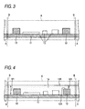
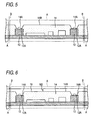
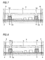
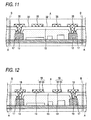
- Figs. 3 to 16 are diagrams showing manufacturing processes of the semiconductor apparatus of the exemplary, non-limiting embodiment.
- the same numerals are assigned to the same components as those of the semiconductor apparatus 10 shown in Fig. 1.
- terminals 12 for via connection are first formed on a substrate 11 formed in a semiconductor apparatus formation region A and subsequently, electronic components 13 are mounted on the substrate 11 (electronic component mounting process).
- the terminals 12 for via connection can be formed by, for example, precipitating a Cu plated film in column shape or installing a columnar Cu material.
- a sealing resin 14 is formed on the substrate 11 so as to cover the terminals 12 for via connection and the electronic components 13 (sealing resin formation process).
- a thickness M1 of the sealing resin 14 can be set at, for example, 1 mm.
- a thickness M3 of the sealing resin 14 on the terminal 12 for via connection can be set at, for example, 200 ⁇ m.
- openings 14A for exposing upper surfaces 12A of the terminals 12 for via connection are formed in the sealing resin 14.
- the openings 14A can be formed by, for example, a laser or a drill.
- a resin layer 15 in which adhesion to a conductive film is higher than that of the sealing resin 14 to the conductive film is formed so as to fill the openings 14A and also cover an upper surface 14B of the sealing resin 14 (resin layer formation process).
- the resin layer 15 for example, an epoxy type resin or a material in which metal particles used as a plating catalyst such as Pd are dispersed in an epoxy type resin can be used.
- a thickness M2 of the resin layer 15 can be set at, for example, 30 ⁇ m to 60 ⁇ m.
- openings 15A for exposing the upper surfaces 12A of the terminals 12 for via connection are formed in the resin layer 15 and subsequently, a surface of the resin layer 15 is roughened.
- the openings 15A can be formed by, for example, a laser or a drill. Also, as roughening treatment of the surface of the resin layer 15, for example, desmear treatment can be used.
- seed layers 32 are formed so as to cover the upper surfaces 12A of the terminals 12 for via connection exposed to the openings 15A and the resin layer 15 in which the openings 15A are formed.
- the seed layers 32 for example, a Cu layer formed by an electroless plating method can be used.
- resist layers 33 having openings 33A corresponding to a shape of a wiring pattern 18 are formed on the seed layers 32.
- conductive films 35 are formed on the seed layers 32 by an electrolytic plating method. As a result of this, vias 17 made of the conductive films 35 and the seed layers 32 are formed in the openings 15A.
- the conductive films 35 for example, a Cu film can be used.
- the resist layers 33 are removed by a resist stripping agent.
- unnecessary seed layers 32 which are not covered with the conductive films 35 are removed (wiring pattern formation process).
- wiring patterns 18 made of the conductive films 35 and the seed layers 32 are formed on the resin layer 15.
- resist layers 36 comprising openings 36A for exposing the connection parts 19 while covering the wiring patterns 18 and the resin layer 15 are formed.
- diffusion preventive films 23 are formed on the connection parts 19.
- an Ni/Au layer (a combination layer of Ni layer disposed on the connection parts 19 and Au layer disposed on the Ni layer) can be used.
- the Ni/Au layer can be formed by, for example, an electrolytic plating method using the connection part 19 as a power feeding layer.
- the resist layers 36 are removed by a resist stripping agent after the diffusion preventive films 23 are formed.
- protective films 21 comprising openings 21A for exposing the diffusion preventive films 23 while covering the wiring patterns 18 and the resin layer 15 are formed (protective film formation process).
- the protective films 21 have films having insulation properties.
- a solder resist can be used as the protective films 21, for example.
- a structure shown in Fig. 15 is cut along dicing positions B and is divided into individual pieces and thereby, the semiconductor apparatus 10 is manufactured.
- the wiring patterns 18 can be formed on the resin layer 15 by disposing a resin layer formation process of forming the resin layer 15 in which adhesion to the conductive films 35 is higher than that of the sealing resin 14 to the conductive films on the sealing resin 14 on which it is difficult to form the conductive films 35.
- Fig. 17 is a sectional view of a semiconductor apparatus according to a second exemplary, non-limiting embodiment of the invention.
- M4 shows a thickness (hereinafter called “thickness M4") of a sealing resin 41
- M5 shows a thickness (hereinafter called “thickness M5") of a resin layer 42, respectively.
- the same numerals are assigned to the same components as those of the semiconductor apparatus 10 of the first exemplary, non-limiting embodiment.
- the semiconductor apparatus 40 has a configuration similar to that of the semiconductor apparatus 10 except that a sealing resin 41, a resin layer 42 and vias 45 are disposed instead of the sealing resin 14, the resin layer 15 and the vias 17 disposed in the semiconductor apparatus 10 of the first exemplary, non-limiting embodiment.
- the sealing resin 41 is a resin having properties similar to those of the sealing resin 14 described in the first exemplary, non-limiting embodiment and is a resin with bad adhesion to a conductive film.
- the sealing resin 41 is disposed on a substrate 11 so as to seal electronic components 13.
- an upper surface 41A of the sealing resin 41 is formed substantially flush with upper surfaces 12A of terminals 12 for via connection. That is, the thickness M4 of the sealing resin 41 is constructed so as to become substantially equal to a height H1 of the terminal 12 for via connection.
- a resin similar to the sealing resin 14 described in the first exemplary, non-limiting embodiment can be used as the sealing resin 41.
- the thickness M4 of the sealing resin 41 can be thinned to achieve miniaturization (thinning) of the semiconductor apparatus 40.
- the resin layer 42 is a resin layer in which adhesion to a conductive film is higher than that of the sealing resin 41 to the conductive film and roughening can be performed to the extent that the conductive film can be formed.
- the resin layer 42 has an opening 42A for exposing the upper surface 12A of the terminal 12 for via connection and is disposed so as to cover an upper surface 41A of the sealing resin 41.
- a resin similar to the resin layer 15 described in the first exemplary, non-limiting embodiment can be used.
- the conductive film also includes a seed layer. Further, an antenna may be formed instead of the wiring pattern 18.
- the conductive film herein means a film constructing a conductive pattern such as the wiring pattern or the antenna, or the seed layer.
- the vias 45 are disposed in the openings 42A formed in the resinlayer42, and make electrical connection between wiring patterns 18 and the terminals 12 for via connection.
- the semiconductor apparatus of the exemplary, non-limiting embodiment by disposing the resin layer 42 in which adhesion to the conductive film is higher than that of the sealing resin 41 to the conductive film on the sealing resin 41 and forming the wiring patterns 18 on the resin layer 42, a mounting density of the semiconductor apparatus 40 can be improved and also, the thickness M4 of the sealing resin 41 can be thinned to achieve miniaturization of the semiconductor apparatus 40.
- an external connection terminal connected to the wiring of the substrate 11 may be disposed in a lower surface of the substrate 11.
- the wiring pattern 18 may be used as a lead line for electrical connection between the electronic components 13.
- Figs. 18 to 22 are diagrams showing manufacturing processes of the semiconductor apparatus of the exemplary, non-limiting embodiment.
- the same numerals are assigned to the same components as those of the semiconductor apparatus 40 described in Fig. 17.
- A1 shows a region (hereinafter called “a semiconductor apparatus formation region A1") in which the semiconductor apparatus 40 is formed
- B1 shows a position (hereinafter called "a dicing position B1") in which a dicing blade cuts, respectively.
- a thickness M5 of the resin layer 42 can be set at, for example, 30 ⁇ m to 60 ⁇ m.
- openings 42A for exposing the upper surfaces 12A of the terminals 12 for via connection are formed in the resin layer 42 and thereafter, a surface of the resin layer 42 in which the openings 42A are formed is roughened.
- the openings 42A can be formed by, for example, a laser or a drill. Also, as roughening treatment of the surface of the resin layer 42, for example, desmear treatment can be used.
- seed layers 32 are formed so as to cover the upper surfaces 12A of the terminals 12 for via connection exposed to the openings 42A and the resin layer 42 in which the openings 42A are formed.
- the seed layers 32 for example, a Cu layer formed by an electroless plating method can be used.
- the semiconductor apparatus 40 comprising vias 45 made of conductive films 35 and the seed layers 32 is manufactured as shown in Fig. 22.
- the thickness M4 of the sealing resin 41 can be thinned to achieve miniaturization of the semiconductor apparatus 40.
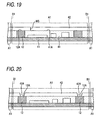
- Fig. 23 is a sectional view of a semiconductor apparatus according to a third exemplary, non-limiting embodiment of the invention.
- M6 shows a thickness (hereinafter called “thickness M6") of a resin layer 52
- M7 shows a thickness (hereinafter called “thickness M7”) of a shielding layer 53, respectively.
- the same numerals are assigned to the same components as those of the semiconductor apparatus 10 of the first exemplary, non-limiting embodiment.
- the semiconductor apparatus 50 has a substrate 11, electronic components 13, a sealing resin 14, a via 17, a ground terminal 51, the resin layer 52, the shielding layer 53 and a protective film 55.
- the ground terminal 51 is a terminal set at a ground potential and is disposed on the substrate 11.
- the ground terminal 51 is electrically connected to the shielding layer 53 through the via 17.
- the resin layer 52 is a resin layer in which adhesion to a conductive film is higher than that of the sealing resin 14 to the conductive film and roughening can be performed to the extent that the conductive film can be formed.
- the resin layer 52 has openings 52A for exposing upper surfaces 51A of the ground terminals 51 and is disposed so as to cover an upper surface 14B and side surfaces 14C of the sealing resin 14.
- As the resin layer 52 a resin similar to the resin layer 15 described in the first exemplary, non-limiting embodiment can be used.
- the thickness M6 of the resin layer 52 can be set at, for example, 30 ⁇ m to 60 ⁇ m.
- the conductive film also includes a seed layer.
- the conductive film herein means a film constructing the shielding layer or the seed layer.
- the shielding layer 53 can be formed so as to continuously surround the upper surface 14B and the side surfaces 14C of the sealing resin 14.
- the shielding layer 53 is disposed on the resin layer 52 so as to continuously surround the upper surface 14B and the side surfaces 14C of the sealing resin 14.
- the shielding layer 53 is electrically connected to the vias 17 and is electrically connected to the ground terminals 51 through the vias 17.
- the shielding layer 53 By disposing the shielding layer 53 so as to surround the upper surface 14B and the side surfaces 14C of the sealing resin 14 for sealing the electronic components 13 thus, electromagnetic waves intruding from the sides of the side surfaces 14C of the sealing resin 14 can be blocked and the electromagnetic waves from the outside can be blocked with high accuracy.
- the shielding layer 53 can be formed by forming a conductive film formed by, for example, a sputtering method, a vacuum evaporation method or a plating method.
- a sputtering method for example, a vacuum evaporation method or a plating method.
- A1 can be used as material of the shielding layer 53.
- the plating method as material of the shielding layer 53, for example, Cu can be used.
- the thickness M7 of the shielding layer 53 can be set at, for example, 10 ⁇ m to 30 ⁇ m.
- the protective film 55 is a film having insulation properties and is disposed so as to cover the shielding layer 53.
- the protective film 55 is a film for protecting the shielding layer 53.
- a solder resist can be used as the protective film 55.
- the electromagnetic waves from the outside can be blocked with high accuracy by disposing the resin layer 52 in which adhesion to the conductive film is higher than that of the sealing resin 14 to the conductive film and roughening can be performed to the extent that the conductive film can be formed so as to cover the sealing resin 14 in which it is difficult to form the conductive film (metal film) and disposing the shielding layer 53 on the resin layer 52 so as to continuously surround the upper surface 14B and the side surfaces 14C of the sealing resin 14.
- the shielding layer 53 and the resin layer 52 may be disposed in only the side of the upper surface 14B of the sealing resin 14.
- an external connection terminal connected to the wiring of the substrate 11 may be disposed in a lower surface of the substrate 11. Further, a substrate comprising a shielding layer in the inside could be used as the substrate 11. Also, the vias 17 may be directly connected to a part of the wiring for ground of the substrate 11 without disposing the ground terminals 51.
- Figs. 24 to 34 are diagrams showing manufacturing processes of the semiconductor apparatus of the exemplary, non-limiting embodiment.
- A2 shows a region (hereinafter called "a semiconductor apparatus formation region A2") in which a semiconductor apparatus 50 is formed, and B2 shows a position (hereinafter called "a dicing position B2") cut by a dicing blade, respectively.
- a dicing position B2 a position cut by a dicing blade
- ground terminals 51 are first formed on a substrate 11 corresponding to the semiconductor apparatus formation region A2 (ground terminal formation process) and subsequently, electronic components 13 are mounted on the substrate 11 (electronic component mounting process).
- a sealing resin 14 is formed on the substrate 11 so as to cover the ground terminals 51 and the electronic components 13 (sealing resin formation process).
- a thickness M8 (thickness ranging from an upper surface 51A of the ground terminal 51 to an upper surface 14B of the sealing resin 14) of the sealing resin 14 can be set at, for example, 200 ⁇ m.
- a groove part 57 for exposing the substrate 11 is formed in the sealing resin 14 corresponding to the dicing position B2.
- the groove part 57 can be formed by, for example, cutting by the dicing blade.
- a width W1 of the groove part 57 can be set at, for example, 0.5 mm.
- openings 14A for exposing the upper surfaces 51A of the ground terminals 51 are formed.
- a resin layer 52 in which adhesion to a conductive film is higher than that of the sealing resin 14 to the conductive film is formed so as to cover the upper surface 14B of the sealing resin 14 while filling the openings 14A and the groove part 57 (resin layer formation process).
- a groove part 59 for exposing an upper surface 11A of the substrate 11 is formed in the resin layer 52 with which the groove part 57 is filled.
- the groove part 59 is formed so that the resin layer 52 remains in side surfaces 14C of the sealing resin 14 (a state of covering the side surfaces 14C of the sealing resin 14 with the resin layer 52).
- the groove part 59 can be formed by, for example, cutting by the dicing blade.
- openings 52A for exposing the upper surfaces 51A of the ground terminals 51 are formed in the resin layer 52 and thereafter, a surface of the resin layer 52 is roughened.
- the openings 52A can be formed by, for example, a laser or a drill. Also, as roughening treatment of the surface of the resin layer 52, for example, desmear treatment can be used.
- seed layers 32 are formed so as to cover the resin layer 52 and the upper surfaces 51A of the ground terminals 51 exposed to the openings 52A.
- the seed layers 32 are power feeding layers in the case of performing electrolytic plating.
- As the seed layers 32 for example, a Cu layer formed by an electroless plating method can be used.
- a conductive film 35 is formed on the seed layers 32.
- vias 17 and a shielding layer 53 for surrounding the upper surface 14B and the side surfaces 14C of the sealing resin 14 are formed in the openings 52A (shielding layer formation process).
- the shielding layer 53 and the vias 17 are made of the seed layer 32 and the conductive film 35, respectively.
- the conductive film 35 for example, a Cu film formed by an electrolytic plating method can be used.
- a protective film 55 is formed so as to cover the shielding layer 53 while filling the groove part 59 (protective film formation process).
- the protective film 55 is a film having insulation properties and protects the shielding layer 53.
- a solder resist can be used as the protective film 55.
- the structure shown in Fig. 33 is cut along the dicing positions B2 and is divided into individual pieces and thereby, the semiconductor apparatus 50 is manufactured.
- the shielding layer 53 can be formed on the resin layer 52 with high accuracy by forming the resin layer 52 in which adhesion to the conductive film is higher than that of the sealing resin 14 to the conductive film so as to cover the sealing resin 14 on which it is difficult to form the conductive film.
- the shielding layer 53 is formed so as to surround the upper surface 14B and the side surfaces 14C of the sealing resin 14 and electromagnetic waves can be blocked with high accuracy.
- the shielding layer 53 may be formed by forming anAl layer by, for example, a sputtering method or a vacuum evaporation method. Also, the shielding layer 53 may be disposed in only the resin layer 52 disposed in the side of the upper surface 14B of the sealing resin 14.
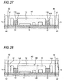
- Fig. 35 is a sectional view of a semiconductor apparatus of a fourth exemplary, non-limiting embodiment.
- H2 shows a height (hereinafter called “height H2") of a ground terminal 51
- M8 shows a thickness (hereinafter called “thickness M8") of a resin layer 63
- M9 shows a thickness (hereinafter called “thickness M9”) of a sealing resin 61, respectively.
- the same numerals are assigned to the same components as those of the semiconductor apparatus 50 of the third exemplary, non-limiting embodiment.
- the semiconductor apparatus 60 has a configuration similar to that of the semiconductor apparatus 50 except that a sealing resin 61, a resin layer 63 and vias 65 are disposed instead of the sealing resin 14, the resin layer 52 and the vias 17 disposed in the semiconductor apparatus 50 of the third exemplary, non-limiting embodiment.
- the sealing resin 61 is disposed on a substrate 11 so as to seal electronic components 13.
- An upper surface 61A of the sealing resin 61 is formed substantially flush with upper surfaces 51A of ground terminals 51. Also, the thickness M9 of the sealing resin 61 is formed substantially equally to the height H2 of the ground terminal 51.
- the sealing resin 61 By forming the upper surface 61A of the sealing resin 61 substantially flush with the upper surfaces 51A of the ground terminals 51 and thinning the thickness M9 of the sealing resin 61 thus, miniaturization (thinning) of the semiconductor apparatus 60 can be achieved.
- the sealing resin 61 a resin similar to the sealing resin 14 described in the first exemplary, non-limiting embodiment can be used.
- the resin layer 63 has an opening 63A for exposing the upper surface 51A of the ground terminal 51 and is disposed so as to cover the upper surface 61A and side surfaces 61B of the sealing resin 61.
- the resin layer 63 is a resin layer in which adhesion to a conductive film is higher than that of the sealing resin 61 to the conductive film and roughening can be performed to the extent that the conductive film can be formed.
- a resin similar to the resin layer 15 described in the first exemplary, non-limiting embodiment can be used.
- the conductive film also includes a seed layer.
- the conductive film herein means a film constructing the shielding layer or the seed layer.
- the vias 65 are disposed in the openings 63A formed in the resin layer 63.
- the vias 65 make electrical connection between a shielding layer 53 and the ground terminals 51.
- electromagnetic waves from the outside are blocked with high accuracy and also the upper surface 61A of the sealing resin 61 is formed substantially flush with the upper surfaces 51A of the ground terminals 51 and the thickness M9 of the sealing resin 61 is thinned and thereby, miniaturization of the semiconductor apparatus 60 can be achieved.
- the shielding layer 53 and the resin layer 63 may be disposed in only the side of the upper surface 61A of the sealing resin 61.
- an external connection terminal connected to the wiring of the substrate 11 may be disposed in a lower surface of the substrate 11. Further, a substrate comprising a shielding layer in the inside could be used as the substrate 11.
- Figs. 36 to 41 are diagrams showing manufacturing processes of the semiconductor apparatus of the exemplary, non-limiting embodiment.
- A3 shows a region (hereinafter called “a semiconductor apparatus formation region A3") in which a semiconductor apparatus 60 is formed, and B3 shows a position (hereinafter called "a dicing position B3") cut by a dicing blade, respectively.
- a semiconductor apparatus formation region A3 a region in which a semiconductor apparatus 60 is formed
- B3 shows a position (hereinafter called "a dicing position B3”) cut by a dicing blade, respectively.
- the same numerals are assigned to the same components as those of the semiconductor apparatus 50 described in Fig. 35.
- ground terminals 51 are formed on a substrate 11 (ground terminal formation process) and subsequently, electronic components 13 are mounted on the substrate 11 (electronic component mounting process). Thereafter, a sealing resin 61 is formed on the substrate 11 so as to cover the ground terminals 51 and the electronic components 13 (sealing resin formation process).
- the sealing resin 61 is polished so that an upper surface 61A of the sealing resin 61 becomes flush with upper surfaces 51A of the ground terminals 51.
- a groove part 62 for exposing an upper surface 11A of the substrate 11 is formed in the sealing resin 61 corresponding to the dicing position B3.
- the groove part 62 can be formed by, for example, cutting by the dicing blade.
- a width W2 of the groove part 62 can be set at, for example, 0.5 mm.
- a resin layer 63 in which adhesion to a conductive film is higher than that of the sealing resin 61 to the conductive film is formed so as to cover the upper surface 61A of the sealing resin 61 while filling the groove part 62 (resin layer formation process).
- the resin layer 63 a resin similar to the resin layer 15 described in the first exemplary, non-limiting embodiment can be used.
- the thickness M8 of the resin layer 63 can be set at, for example, 30 ⁇ m to 60 ⁇ m.
- a groove part 64 for exposing the upper surface 11A of the substrate 11 is formed in the resin layer 63 with which the groove part 62 of the sealing resin 61 is filled.
- the groove part 64 is formed so that the resin layer 63 remains in side surfaces 61B of the sealing resin 61 (a state of covering the side surfaces 61B of the sealing resin 61 with the resin layer 63).
- the groove part 64 can be formed by, for example, cutting by the dicing blade.
- openings 63A for exposing the upper surfaces 51A of the ground terminals 51 are formed in the resin layer 63 and thereafter, a surface of the resin layer 63 is roughened.
- the openings 63A can be formed by, for example, a laser or a drill. Also, as roughening treatment of the surface of the resin layer 63, for example, desmear treatment can be used.
- the semiconductor apparatus 60 is manufactured as shown in Fig. 41.
- the sealing resin 61 is polished so that the upper surface 61A of the sealing resin 61 becomes flush with the upper surfaces 51A of the ground terminals 51 and thereby, the thickness M9 of the sealing resin 61 can be thinned to achieve miniaturization of the semiconductor apparatus 60.
- the shielding layer 53 may be disposed in only the resin layer 63 disposed in the side of the upper surface 61A of the sealing resin 61.
Landscapes
- Structures Or Materials For Encapsulating Or Coating Semiconductor Devices Or Solid State Devices (AREA)
- Encapsulation Of And Coatings For Semiconductor Or Solid State Devices (AREA)
- Non-Metallic Protective Coatings For Printed Circuits (AREA)
- Shielding Devices Or Components To Electric Or Magnetic Fields (AREA)
- Structure Of Printed Boards (AREA)
Applications Claiming Priority (1)
| Application Number | Priority Date | Filing Date | Title |
|---|---|---|---|
| JP2005132539A JP4589170B2 (ja) | 2005-04-28 | 2005-04-28 | 半導体装置及びその製造方法 |
Publications (3)
| Publication Number | Publication Date |
|---|---|
| EP1717857A2 true EP1717857A2 (fr) | 2006-11-02 |
| EP1717857A3 EP1717857A3 (fr) | 2008-03-26 |
| EP1717857B1 EP1717857B1 (fr) | 2016-08-31 |
Family
ID=36601145
Family Applications (1)
| Application Number | Title | Priority Date | Filing Date |
|---|---|---|---|
| EP06252231.3A Ceased EP1717857B1 (fr) | 2005-04-28 | 2006-04-26 | Dispositf semi-conducteur et méthode de fabrication associée |
Country Status (6)
| Country | Link |
|---|---|
| US (1) | US7514772B2 (fr) |
| EP (1) | EP1717857B1 (fr) |
| JP (1) | JP4589170B2 (fr) |
| KR (1) | KR20060113412A (fr) |
| CN (1) | CN1855451B (fr) |
| TW (1) | TW200644297A (fr) |
Cited By (12)
| Publication number | Priority date | Publication date | Assignee | Title |
|---|---|---|---|---|
| WO2009003018A3 (fr) * | 2007-06-27 | 2009-01-29 | Rf Micro Devices Inc | Procédé de protection conforme utilisant des gaz de procédé |
| US8053872B1 (en) * | 2007-06-25 | 2011-11-08 | Rf Micro Devices, Inc. | Integrated shield for a no-lead semiconductor device package |
| US8062930B1 (en) | 2005-08-08 | 2011-11-22 | Rf Micro Devices, Inc. | Sub-module conformal electromagnetic interference shield |
| US8835226B2 (en) | 2011-02-25 | 2014-09-16 | Rf Micro Devices, Inc. | Connection using conductive vias |
| US8959762B2 (en) | 2005-08-08 | 2015-02-24 | Rf Micro Devices, Inc. | Method of manufacturing an electronic module |
| US9137934B2 (en) | 2010-08-18 | 2015-09-15 | Rf Micro Devices, Inc. | Compartmentalized shielding of selected components |
| US9627230B2 (en) | 2011-02-28 | 2017-04-18 | Qorvo Us, Inc. | Methods of forming a microshield on standard QFN package |
| US9807890B2 (en) | 2013-05-31 | 2017-10-31 | Qorvo Us, Inc. | Electronic modules having grounded electromagnetic shields |
| US11058038B2 (en) | 2018-06-28 | 2021-07-06 | Qorvo Us, Inc. | Electromagnetic shields for sub-modules |
| US11114363B2 (en) | 2018-12-20 | 2021-09-07 | Qorvo Us, Inc. | Electronic package arrangements and related methods |
| US11127689B2 (en) | 2018-06-01 | 2021-09-21 | Qorvo Us, Inc. | Segmented shielding using wirebonds |
| US11515282B2 (en) | 2019-05-21 | 2022-11-29 | Qorvo Us, Inc. | Electromagnetic shields with bonding wires for sub-modules |
Families Citing this family (21)
| Publication number | Priority date | Publication date | Assignee | Title |
|---|---|---|---|---|
| JP2007036571A (ja) * | 2005-07-26 | 2007-02-08 | Shinko Electric Ind Co Ltd | 半導体装置及びその製造方法 |
| JP4983219B2 (ja) * | 2006-11-22 | 2012-07-25 | 株式会社村田製作所 | 部品内蔵基板 |
| JP2009016371A (ja) * | 2007-06-29 | 2009-01-22 | Casio Comput Co Ltd | シールド機能付きモジュールの製造方法 |
| US7851894B1 (en) * | 2008-12-23 | 2010-12-14 | Amkor Technology, Inc. | System and method for shielding of package on package (PoP) assemblies |
| JP5360221B2 (ja) * | 2009-09-16 | 2013-12-04 | 株式会社村田製作所 | 電子部品内蔵モジュール |
| CN102804430B (zh) * | 2010-01-19 | 2015-11-25 | Lg伊诺特有限公司 | 封装结构及其制造方法 |
| JP5182448B2 (ja) * | 2010-02-18 | 2013-04-17 | 株式会社村田製作所 | 部品内蔵基板 |
| JP2012114173A (ja) * | 2010-11-23 | 2012-06-14 | Shinko Electric Ind Co Ltd | 半導体装置の製造方法及び半導体装置 |
| CN102479773A (zh) * | 2010-11-26 | 2012-05-30 | 海华科技股份有限公司 | 具有电性屏蔽功能的模块集成电路封装结构及其制作方法 |
| TW201225242A (en) * | 2010-12-03 | 2012-06-16 | Azurewave Technologies Inc | Module IC package structure and method of making the same |
| CN102543904A (zh) * | 2010-12-16 | 2012-07-04 | 海华科技股份有限公司 | 模块集成电路封装结构及其制作方法 |
| JP6050975B2 (ja) * | 2012-03-27 | 2016-12-21 | 新光電気工業株式会社 | リードフレーム、半導体装置及びリードフレームの製造方法 |
| JP5952074B2 (ja) | 2012-04-27 | 2016-07-13 | ラピスセミコンダクタ株式会社 | 半導体装置及び計測機器 |
| KR20140119522A (ko) * | 2013-04-01 | 2014-10-10 | 삼성전자주식회사 | 패키지-온-패키지 구조를 갖는 반도체 패키지 |
| CN107501870A (zh) * | 2015-10-27 | 2017-12-22 | 张荣斌 | 防静电阻燃电路板用密封层材料 |
| CN105873369B (zh) * | 2016-05-19 | 2019-05-31 | 北京奇虎科技有限公司 | 一种印制电路板的制作方法和印制电路板 |
| TWM551755U (zh) * | 2017-06-20 | 2017-11-11 | 長華科技股份有限公司 | 泛用型導線架 |
| JP6752768B2 (ja) * | 2017-10-17 | 2020-09-09 | 矢崎総業株式会社 | フィルムアンテナ |
| KR102145218B1 (ko) * | 2018-08-07 | 2020-08-18 | 삼성전자주식회사 | 팬-아웃 반도체 패키지 |
| KR102749213B1 (ko) * | 2019-12-27 | 2025-01-03 | 삼성전자주식회사 | 반도체 패키지 및 그의 제조 방법 |
| WO2021205930A1 (fr) * | 2020-04-07 | 2021-10-14 | 株式会社村田製作所 | Module |
Family Cites Families (14)
| Publication number | Priority date | Publication date | Assignee | Title |
|---|---|---|---|---|
| JPH02125498A (ja) * | 1988-11-04 | 1990-05-14 | Hitachi Chem Co Ltd | 高密度配線板およびその製造法 |
| JPH06502744A (ja) * | 1991-03-27 | 1994-03-24 | インテグレイテッド システム アセンブリース コーポレーション | マルチチップ集積回路パッケージ及びモジュール |
| TW293232B (fr) | 1995-02-23 | 1996-12-11 | Hitachi Ltd | |
| JP2734424B2 (ja) * | 1995-08-16 | 1998-03-30 | 日本電気株式会社 | 半導体装置 |
| JP3644662B2 (ja) * | 1997-10-29 | 2005-05-11 | 株式会社ルネサステクノロジ | 半導体モジュール |
| US6117536A (en) | 1998-09-10 | 2000-09-12 | Ga-Tek Inc. | Adhesion promoting layer for use with epoxy prepregs |
| JP2000223647A (ja) * | 1999-02-03 | 2000-08-11 | Murata Mfg Co Ltd | 高周波モジュールの製造方法 |
| JP4029517B2 (ja) * | 1999-03-31 | 2008-01-09 | 株式会社日立製作所 | 配線基板とその製造方法及び半導体装置 |
| EP1126321A1 (fr) * | 2000-02-10 | 2001-08-22 | Shipley Company LLC | Photoréserve de type positif contenant des polymères réticulés |
| JP2001244688A (ja) * | 2000-02-28 | 2001-09-07 | Kyocera Corp | 高周波モジュール部品及びその製造方法 |
| JP3553849B2 (ja) * | 2000-03-07 | 2004-08-11 | 富士電機デバイステクノロジー株式会社 | 半導体装置及びその製造方法 |
| JP3951091B2 (ja) * | 2000-08-04 | 2007-08-01 | セイコーエプソン株式会社 | 半導体装置の製造方法 |
| JP3718131B2 (ja) * | 2001-03-16 | 2005-11-16 | 松下電器産業株式会社 | 高周波モジュールおよびその製造方法 |
| JP2005109306A (ja) * | 2003-10-01 | 2005-04-21 | Matsushita Electric Ind Co Ltd | 電子部品パッケージおよびその製造方法 |
-
2005
- 2005-04-28 JP JP2005132539A patent/JP4589170B2/ja not_active Expired - Fee Related
-
2006
- 2006-04-20 KR KR1020060035694A patent/KR20060113412A/ko not_active Withdrawn
- 2006-04-25 US US11/380,128 patent/US7514772B2/en active Active
- 2006-04-26 EP EP06252231.3A patent/EP1717857B1/fr not_active Ceased
- 2006-04-28 TW TW095115253A patent/TW200644297A/zh unknown
- 2006-04-28 CN CN200610076530XA patent/CN1855451B/zh not_active Expired - Fee Related
Cited By (28)
| Publication number | Priority date | Publication date | Assignee | Title |
|---|---|---|---|---|
| US8062930B1 (en) | 2005-08-08 | 2011-11-22 | Rf Micro Devices, Inc. | Sub-module conformal electromagnetic interference shield |
| US8959762B2 (en) | 2005-08-08 | 2015-02-24 | Rf Micro Devices, Inc. | Method of manufacturing an electronic module |
| US9661739B2 (en) | 2005-08-08 | 2017-05-23 | Qorvo Us, Inc. | Electronic modules having grounded electromagnetic shields |
| US8349659B1 (en) | 2007-06-25 | 2013-01-08 | Rf Micro Devices, Inc. | Integrated shield for a no-lead semiconductor device package |
| US8053872B1 (en) * | 2007-06-25 | 2011-11-08 | Rf Micro Devices, Inc. | Integrated shield for a no-lead semiconductor device package |
| US8186048B2 (en) | 2007-06-27 | 2012-05-29 | Rf Micro Devices, Inc. | Conformal shielding process using process gases |
| US8296941B2 (en) | 2007-06-27 | 2012-10-30 | Rf Micro Devices, Inc. | Conformal shielding employing segment buildup |
| US8296938B2 (en) | 2007-06-27 | 2012-10-30 | Rf Micro Devices, Inc. | Method for forming an electronic module having backside seal |
| US8220145B2 (en) | 2007-06-27 | 2012-07-17 | Rf Micro Devices, Inc. | Isolated conformal shielding |
| US8359739B2 (en) | 2007-06-27 | 2013-01-29 | Rf Micro Devices, Inc. | Process for manufacturing a module |
| US8409658B2 (en) | 2007-06-27 | 2013-04-02 | Rf Micro Devices, Inc. | Conformal shielding process using flush structures |
| US8434220B2 (en) | 2007-06-27 | 2013-05-07 | Rf Micro Devices, Inc. | Heat sink formed with conformal shield |
| US8614899B2 (en) | 2007-06-27 | 2013-12-24 | Rf Micro Devices, Inc. | Field barrier structures within a conformal shield |
| US8720051B2 (en) | 2007-06-27 | 2014-05-13 | Rf Micro Devices, Inc. | Conformal shielding process using process gases |
| WO2009003018A3 (fr) * | 2007-06-27 | 2009-01-29 | Rf Micro Devices Inc | Procédé de protection conforme utilisant des gaz de procédé |
| US8061012B2 (en) | 2007-06-27 | 2011-11-22 | Rf Micro Devices, Inc. | Method of manufacturing a module |
| US9137934B2 (en) | 2010-08-18 | 2015-09-15 | Rf Micro Devices, Inc. | Compartmentalized shielding of selected components |
| US8835226B2 (en) | 2011-02-25 | 2014-09-16 | Rf Micro Devices, Inc. | Connection using conductive vias |
| US9420704B2 (en) | 2011-02-25 | 2016-08-16 | Qorvo Us, Inc. | Connection using conductive vias |
| US9942994B2 (en) | 2011-02-25 | 2018-04-10 | Qorvo Us, Inc. | Connection using conductive vias |
| US9627230B2 (en) | 2011-02-28 | 2017-04-18 | Qorvo Us, Inc. | Methods of forming a microshield on standard QFN package |
| US9807890B2 (en) | 2013-05-31 | 2017-10-31 | Qorvo Us, Inc. | Electronic modules having grounded electromagnetic shields |
| US11127689B2 (en) | 2018-06-01 | 2021-09-21 | Qorvo Us, Inc. | Segmented shielding using wirebonds |
| US11058038B2 (en) | 2018-06-28 | 2021-07-06 | Qorvo Us, Inc. | Electromagnetic shields for sub-modules |
| US11219144B2 (en) | 2018-06-28 | 2022-01-04 | Qorvo Us, Inc. | Electromagnetic shields for sub-modules |
| US11114363B2 (en) | 2018-12-20 | 2021-09-07 | Qorvo Us, Inc. | Electronic package arrangements and related methods |
| US11515282B2 (en) | 2019-05-21 | 2022-11-29 | Qorvo Us, Inc. | Electromagnetic shields with bonding wires for sub-modules |
| US12431457B2 (en) | 2019-05-21 | 2025-09-30 | Qorvo Us, Inc. | Electromagnetic shields with bonding wires for sub-modules |
Also Published As
| Publication number | Publication date |
|---|---|
| JP2006310629A (ja) | 2006-11-09 |
| CN1855451B (zh) | 2010-06-23 |
| US20060244131A1 (en) | 2006-11-02 |
| KR20060113412A (ko) | 2006-11-02 |
| TW200644297A (en) | 2006-12-16 |
| CN1855451A (zh) | 2006-11-01 |
| JP4589170B2 (ja) | 2010-12-01 |
| EP1717857A3 (fr) | 2008-03-26 |
| US7514772B2 (en) | 2009-04-07 |
| EP1717857B1 (fr) | 2016-08-31 |
Similar Documents
| Publication | Publication Date | Title |
|---|---|---|
| EP1717857B1 (fr) | Dispositf semi-conducteur et méthode de fabrication associée | |
| EP2592915B1 (fr) | Procédé de fabrication pour carte de câblage laminée | |
| US10714822B2 (en) | Wireless module and method for manufacturing wireless module | |
| US10665936B2 (en) | Wireless module and method for manufacturing wireless module | |
| US8035192B2 (en) | Semiconductor device and manufacturing method thereof | |
| US20130155639A1 (en) | Electronic component and method for manufacturing the same | |
| US11382207B2 (en) | Electronic device module and method of manufacturing electronic device module | |
| EP2009692A1 (fr) | Module électronique et son procédé de fabrication | |
| US20070231962A1 (en) | Manufacturing method of wiring substrate and manufacturing method of semiconductor device | |
| US20070052083A1 (en) | Semiconductor package and manufacturing method thereof | |
| US20090288873A1 (en) | Wiring board and method of manufacturing the same | |
| JP5441007B2 (ja) | 電子部品内蔵基板の製造方法 | |
| US20080272469A1 (en) | Semiconductor die package and integrated circuit package and fabricating method thereof | |
| US20070023888A1 (en) | Semiconductor device and manufacturing method thereof | |
| US9281260B2 (en) | Semiconductor packages and methods of forming the same | |
| CN106328633B (zh) | 电子装置模块及其制造方法 | |
| US7772109B2 (en) | Manufacturing method of multilayer wiring substrate | |
| JP2006294701A (ja) | 半導体装置及びその製造方法 | |
| CN113555347A (zh) | 电子器件模块及制造该电子器件模块的方法 | |
| US8603858B2 (en) | Method for manufacturing a semiconductor package | |
| US20170263571A1 (en) | Electronic component built-in substrate and method for manufacturing the same | |
| WO2017122284A1 (fr) | Substrat à composant incorporé et procédé de fabrication de substrat à composant incorporé | |
| US20250372561A1 (en) | Semiconductor device and method of manufacturing semiconductor device | |
| JP2014027311A (ja) | 電子部品内蔵基板の製造方法 | |
| KR20170076409A (ko) | 인쇄회로기판 |
Legal Events
| Date | Code | Title | Description |
|---|---|---|---|
| PUAI | Public reference made under article 153(3) epc to a published international application that has entered the european phase |
Free format text: ORIGINAL CODE: 0009012 |
|
| AK | Designated contracting states |
Kind code of ref document: A2 Designated state(s): AT BE BG CH CY CZ DE DK EE ES FI FR GB GR HU IE IS IT LI LT LU LV MC NL PL PT RO SE SI SK TR |
|
| AX | Request for extension of the european patent |
Extension state: AL BA HR MK YU |
|
| PUAL | Search report despatched |
Free format text: ORIGINAL CODE: 0009013 |
|
| AK | Designated contracting states |
Kind code of ref document: A3 Designated state(s): AT BE BG CH CY CZ DE DK EE ES FI FR GB GR HU IE IS IT LI LT LU LV MC NL PL PT RO SE SI SK TR |
|
| AX | Request for extension of the european patent |
Extension state: AL BA HR MK YU |
|
| 17P | Request for examination filed |
Effective date: 20080924 |
|
| AKX | Designation fees paid |
Designated state(s): FR |
|
| REG | Reference to a national code |
Ref country code: DE Ref legal event code: 8566 |
|
| 17Q | First examination report despatched |
Effective date: 20090731 |
|
| GRAP | Despatch of communication of intention to grant a patent |
Free format text: ORIGINAL CODE: EPIDOSNIGR1 |
|
| INTG | Intention to grant announced |
Effective date: 20160404 |
|
| GRAS | Grant fee paid |
Free format text: ORIGINAL CODE: EPIDOSNIGR3 |
|
| GRAA | (expected) grant |
Free format text: ORIGINAL CODE: 0009210 |
|
| AK | Designated contracting states |
Kind code of ref document: B1 Designated state(s): FR |
|
| REG | Reference to a national code |
Ref country code: FR Ref legal event code: PLFP Year of fee payment: 12 |
|
| PLBE | No opposition filed within time limit |
Free format text: ORIGINAL CODE: 0009261 |
|
| STAA | Information on the status of an ep patent application or granted ep patent |
Free format text: STATUS: NO OPPOSITION FILED WITHIN TIME LIMIT |
|
| 26N | No opposition filed |
Effective date: 20170601 |
|
| REG | Reference to a national code |
Ref country code: FR Ref legal event code: PLFP Year of fee payment: 13 |
|
| PGFP | Annual fee paid to national office [announced via postgrant information from national office to epo] |
Ref country code: FR Payment date: 20190313 Year of fee payment: 14 |
|
| PG25 | Lapsed in a contracting state [announced via postgrant information from national office to epo] |
Ref country code: FR Free format text: LAPSE BECAUSE OF NON-PAYMENT OF DUE FEES Effective date: 20200430 |