EP1720190A2 - Ecran plasma, sa méthode de fabrication et la composition de ses parois séparatrices - Google Patents
Ecran plasma, sa méthode de fabrication et la composition de ses parois séparatrices Download PDFInfo
- Publication number
- EP1720190A2 EP1720190A2 EP06290676A EP06290676A EP1720190A2 EP 1720190 A2 EP1720190 A2 EP 1720190A2 EP 06290676 A EP06290676 A EP 06290676A EP 06290676 A EP06290676 A EP 06290676A EP 1720190 A2 EP1720190 A2 EP 1720190A2
- Authority
- EP
- European Patent Office
- Prior art keywords
- display panel
- plasma display
- partition
- set forth
- weight ratio
- Prior art date
- Legal status (The legal status is an assumption and is not a legal conclusion. Google has not performed a legal analysis and makes no representation as to the accuracy of the status listed.)
- Withdrawn
Links
Images


Classifications
-
- H—ELECTRICITY
- H01—ELECTRIC ELEMENTS
- H01J—ELECTRIC DISCHARGE TUBES OR DISCHARGE LAMPS
- H01J11/00—Gas-filled discharge tubes with alternating current induction of the discharge, e.g. alternating current plasma display panels [AC-PDP]; Gas-filled discharge tubes without any main electrode inside the vessel; Gas-filled discharge tubes with at least one main electrode outside the vessel
- H01J11/10—AC-PDPs with at least one main electrode being out of contact with the plasma
- H01J11/12—AC-PDPs with at least one main electrode being out of contact with the plasma with main electrodes provided on both sides of the discharge space
-
- H—ELECTRICITY
- H01—ELECTRIC ELEMENTS
- H01J—ELECTRIC DISCHARGE TUBES OR DISCHARGE LAMPS
- H01J11/00—Gas-filled discharge tubes with alternating current induction of the discharge, e.g. alternating current plasma display panels [AC-PDP]; Gas-filled discharge tubes without any main electrode inside the vessel; Gas-filled discharge tubes with at least one main electrode outside the vessel
- H01J11/20—Constructional details
- H01J11/34—Vessels, containers or parts thereof, e.g. substrates
- H01J11/36—Spacers, barriers, ribs, partitions or the like
-
- H—ELECTRICITY
- H01—ELECTRIC ELEMENTS
- H01J—ELECTRIC DISCHARGE TUBES OR DISCHARGE LAMPS
- H01J9/00—Apparatus or processes specially adapted for the manufacture, installation, removal, maintenance of electric discharge tubes, discharge lamps, or parts thereof; Recovery of material from discharge tubes or lamps
- H01J9/24—Manufacture or joining of vessels, leading-in conductors or bases
- H01J9/241—Manufacture or joining of vessels, leading-in conductors or bases the vessel being for a flat panel display
- H01J9/242—Spacers between faceplate and backplate
-
- H—ELECTRICITY
- H01—ELECTRIC ELEMENTS
- H01J—ELECTRIC DISCHARGE TUBES OR DISCHARGE LAMPS
- H01J2211/00—Plasma display panels with alternate current induction of the discharge, e.g. AC-PDPs
- H01J2211/20—Constructional details
- H01J2211/34—Vessels, containers or parts thereof, e.g. substrates
- H01J2211/36—Spacers, barriers, ribs, partitions or the like
- H01J2211/366—Spacers, barriers, ribs, partitions or the like characterized by the material
Definitions
- the present invention relates to a plasma display panel, and more particularly, to a plasma display panel in which discoloration into yellow color of partitions generated when forming electrodes is prevented, and a method of manufacturing the same.
- partitions formed between a front substrate and a rear substrate, separate respective unit cells.
- the respective unit cells are filled with main discharging gas such as neon gas, helium gas, or a mixture of the neon gas, and the helium gas and inert gas containing a small amount of xenon gas.
- main discharging gas such as neon gas, helium gas, or a mixture of the neon gas
- the helium gas and inert gas containing a small amount of xenon gas.
- the inert gas When electrical discharge is generated due to application of high frequency electric voltage, the inert gas generates vacuum ultraviolet rays to illuminate phosphor so that images are displayed. Since the above-described plasma display panel can be made thin and light in weight, the plasma display panel is standing in the spotlight as a next generation display device.
- FIG. 1 is a schematic perspective view illustrating a conventional plasma display panel.
- a front glass 101 as a displaying surface, where an image is displayed, of a front substrate 100 of the conventional plasma display panel, a plurality of pairs of sustain electrodes, in which pairs of a scan electrode 102 and a sustain electrode 103 are formed, is arranged.
- a plurality of address electrodes 113 is arranged on a rear glass 111 to cross the plural pairs of the sustain electrodes, and the rear substrate 110 is coupled with the front substrate 100 in parallel while keeping a predetermined distance therebetween.
- stripe type (or well type) partitions 112 are arranged to form a plurality electrically-discharging spaces, that is, electrically-discharging cells and keep the parallelism thereof.
- a plurality of address electrodes 113 is disposed in parallel to the partitions to perform the address discharge and to generate vacuum ultraviolet rays.
- the upper surface of the rear substrate 110 is coated with R-, G-, and B-colored phosphor 114 for emitting visual radiation so as to display images when the address discharging is carried out. Between the address electrodes 113 and the phosphor 114, a lower dielectric material layer 115 is formed to protect the address electrodes 113.
- the conventional plasma display panel having the above-described structure is manufactured by the process roughly including a glass fabricating process, a front substrate fabricating process, a rear substrate fabricating process, and an assembling process.
- the process of fabricating the substrate includes a process of forming a scan electrode and a sustain electrode on the front glass, a process of forming an upper dielectric material layer for restricting electric current discharged by the scan electrode and the sustain electrode and for insulating between the pair of the electrodes, and a process of forming a vapor-deposition protective layer of magnesium oxide on the upper dielectric material layer to aid electrical discharge.
- the rear substrate fabricating process includes a process of forming an address electrode on the rear glass, a process of forming a lower dielectric material layer for protecting the address electrode, a process of forming partitions on the upper side of the lower dielectric material layer to partition discharge cells, and a process of forming a phosphor layer between the partitions to emit visual radiation for displaying images.
- the plasma display panel manufactured by the above-described process has shortcomings as follows.
- silver contained in the address electrodes is diffused to the partitions so that the yellow discoloration occurs.
- silver ions (Ag + ) react with alkali components such as sodium ions (Na + ) at the surfaces of the paste of the partitions so that the yellow discoloration occurs.
- alkali components such as sodium ions (Na + )
- the partitions containing unleaded material contain more of the alkali component such as sodium, the yellow discoloration is more serious.
- the diffusion of the silver ions as a reason of the yellow discoloration is further activated due to oxygen (O 2 ) around the electrodes as temperature is gradually increased.
- Temperature when the diffusion begins is about 200 degrees centigrade to 300 degrees centigrade, particularly the diffusion is further activated at 350 degrees centigrade to 400 degrees centigrade.
- the baking process of the partition paste or green sheet is generally carried out at 500 degrees centigrade to 600 degrees centigrade. Due to oxygen in air and temperature higher than 500 degrees centigrade, the diffusion of the silver ions is further activated, so that the yellow discoloration is generated due to surface plasma resonance.
- present invention is directed to a plasma display panel, a method of manufacturing the same, and material for partitions of the plasma display panel that substantially obviate one or more problems due to limitations and disadvantages of the related art.
- An object of the present invention is to provide a plasma display panel in which the yellow discoloration caused by diffusion of silver ions is prevented to improve color temperature of white ray and image quality, a method of manufacturing the same, and material for partitions of the plasma display panel.
- a plasma display panel includes an upper plate having a sustain electrode, a lower plate having an address electrode, and a partition formed between the upper plate and the lower plate and having an inorganic ion exchanger.
- a method of manufacturing a plasma display panel includes the steps of (1) preparing a material for a partition including an inorganic powder having a weight ratio of 60% to 80% and a vehicle having a weight ratio of 20% to 40% and an inorganic ion exchanger having a weight ratio of 0.01% to 5%, and (2) forming the partition on a lower plate using the material for the partition.
- a method of manufacturing a plasma display panel includes the steps of forming a partition including a glass having inorganic powder on a dielectric material of a lower plate, and forming a partition protective layer on the surface of the partition using a material including a solvent having a weight ratio of 80% to 95%, a binder having a weight ratio of 5% to 20%, a dispersant having a weight ratio of 0.1% to 1%, and an inorganic ion exchanger having a weight ratio of 0.01% to 5%.
- a composition of a material for a partition of a plasma display panel comprises an inorganic powder having a weight ratio of 60% to 80%, a vehicle having a weight ratio of 20% to 40%, and an inorganic ion exchanger having a weight ratio of 0.01% to 5%.
- FIG. 1 is a schematic perspective view illustrating a conventional plasma display panel
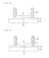
- FIG. 2 is a sectional view schematically illustrating a rear substrate of a plasma display panel according to a first preferred embodiment of the present invention
- FIG. 3 is a sectional view schematically illustrating a rear substrate of a plasma display panel according to a second preferred embodiment of the present invention
- FIG. 4 is a view illustrating composition of material of partitions for the plasma display panel according to the preferred embodiment of the present invention.
- FIG. 5 is a view illustrating composition of material of partition protection layers for the plasma display panel according to the preferred embodiment of the present invention.
- FIG. 6 is a flowchart illustrating a method of manufacturing a plasma display panel according to a first preferred embodiment of the present invention
- FIGS. 7A to 7J are views illustrating the method of manufacturing a plasma display panel according to the first preferred embodiment of the present invention.
- FIG. 8 is a flowchart illustrating a method of manufacturing a plasma display panel according to a second preferred embodiment of the present invention.
- FIGS. 9A to 9K are views illustrating the method of manufacturing a plasma display panel according to the second preferred embodiment of the present invention.
- FIGS. 1 to 9K Reference will now be made in detail to the preferred embodiments of a plasma display panel, a method of manufacturing the same, and material for partitions of the plasma display panel of the present invention, examples of which are illustrated in FIGS. 1 to 9K.
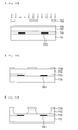
- FIG. 2 is a sectional view schematically illustrating a rear substrate of a plasma display panel according to a first preferred embodiment of the present invention.
- a front substrate of a plasma display panel has the same structure of that of the conventional plasma display panel such that a plurality of pairs of sustain electrodes in which pairs of a scan electrode and a sustain electrode are formed is arranged on a front glass 101 as a displaying surface, where an image is displayed, of a front substrate of the conventional plasma display panel.
- a plurality of address electrodes 113 is arranged on a rear glass 111 to cross the plural pairs of the sustain electrodes.
- a rear substrate 110 is coupled with the front substrate 100 in parallel while keeping a predetermined distance therebetween.
- the rear substrate is formed with partitions 112a to respectively define R-, G-, and B-discharge cells.
- the partitions 112a contain inorganic ion exchangers.
- the partitions 112a are characterized in that inorganic powder has a weight ratio of 95% to 99.99%, the inorganic ion exchangers have a weight ratio of 0.01% to 5%, and more preferably 0.1% to 5%.
- the inorganic powder contains glass with a weight of 50% to 70% and filler with a weight ratio of 30% to 50%.
- the glass contains BiO 3 , B 2 O 3 , SiO 2 , Al 2 O 3 , SrO, BaO, Li 2 O, Na 2 O, K 2 O, CuO, and CeO 2 , wherein, preferably, BiO 3 has a weight ratio of 20% to 60%, B 2 O 3 has a weight ratio of 20% to 55%, SiO 2 has a weight ratio of 0% to 15%, Al 2 O 3 has a weight ratio of 0% to 15%, SrO has a weight ratio of 0% to 30%, BaO has a weight ratio of 0% to 30%, Li 2 O has a weight ratio of 0% to 10%, Na 2 O has a weight ratio of 0% to 10%, K 2 O has a weight ratio of 0% to 10%, CuO has a weight ratio of 0% to 5%, and CeO 2 has a weight ratio of 0% to 5%.
- BiO 3 has a weight ratio of 20% to 60%
- B 2 O 3 has a weight ratio of 20% to 55%
- SiO 2 has a weight
- the partitions contain the inorganic ion exchangers to reduce the quantity of Na + ions that react with Ag + ions.
- the filler preferably contains Al 2 O 3 , TiO 2 , PbO, and ZnO, and the contents of the elements are different from each other according to methods of forming the partitions.
- the quantities of Al 2 O 3 and TiO are relatively much more when the partitions are developed by sanding method, and the quantities of PbO and ZnO are relatively much more when the partitions are developed by etching method.
- the inorganic ion exchangers are selected from at least one of aluminosilicate, hydrous metal oxide, acid salt, heteropolyacid, Ca 10 (PO 4 ) 6 (OH) 2 and MgCl (CO 3 ) (OH)•nH 2 O.
- aluminosilicate is zeolite
- hydrous metal oxide is at least one of Sb 2 O 5 •2H 2 O and Bi 2 O 3 •3H 2 O
- acid salt is at least one of Zr(HPO 4 ) 2 •H 2 O and Ti(HPO 4 ) 2 •H 2 O
- heteropolyacid is (NH 4 ) 3 Mo 12 (PO 4 ) 40 •nH 2 O.
- FIG. 3 is a sectional view schematically illustrating a rear substrate of a plasma display panel according to a second preferred embodiment of the present invention.
- the plasma display panel according to this preferred embodiment is identical to the plasma display panel according to the first preferred embodiment of the present invention, and is different from the same in view that the inorganic exchangers contained in the partitions 112 form separate layers 112b.
- the partitions 112 are formed to contain the inorganic powder and the filler, and in the partitions 112 the inorganic exchangers 112b form the separate layer.
- Composition of the inorganic powder and the filler forming the partitions 112 is not significantly different from the composition of the inorganic powder and the filler in the first preferred embodiment of the present invention, but does not contain the inorganic ion exchangers.
- the inorganic ion exchangers 112b are separately formed in the form of layers formed in the surfaces of the partitions 112. Details for the inorganic exchangers such as kind of the inorganic ion exchangers are identical to those of the inorganic ion exchangers in the first preferred embodiment.
- the plasma display panels including the partitions according to the first and the second preferred embodiments of the present invention further include the inorganic ion exchangers in the partitions or in the surfaces of the partitions.
- the inorganic ion exchangers capture Na + so that the quantity of Na + to react with Ag + is reduced.
- the quantity of Ag + reduced to Ag 0 decreases to prevent the yellow discoloration of the partitions so that color temperature of the white ray of the plasma display panel is improved and light permeability can be improved.
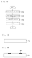
- FIG. 4 is a view illustrating composition of material of partitions for the plasma display panel according to the preferred embodiment of the present invention.
- Composition of material for the partitions of the plasma display panel contains inorganic powder 400, vehicles 410, and inorganic ion exchangers 420.
- the inorganic powder 400 has a weight ratio of 60% to 80%
- the vehicles 410 have a weight ratio of 0% to 40%
- the inorganic ion exchangers 420 have a weight ratio of 0.01% to 5%.
- the inorganic powder 400 contains glass having a weight ratio of 50% to 70% and filler having a weight ratio of 30% to 40%.
- the glass contains Bi2O3, B 2 O 3 , SiO 2 , Al 2 O 3 , SrO, BaO, Li 2 O, Na 2 O, K 2 O, CuO, and CeO 2 .
- composition ratios of Bi 2 O 3 , and the others are identical to those of the plasma display panel according to the first preferred embodiment of the present invention.
- the filler preferably contains A1203, TiO2, PbO, and ZnO, and their respective contents are identical to those as described above even though the method of forming the partitions is different from the method of forming the partitions of the plasma display panel as described above.
- the inorganic ion exchangers 420 are selected from at least one of aluminosilicate, hydrous metal oxide, acid salt, heteropolyacid, Ca 10 (PO 4 ) 6 (OH) 2 and MgCl (CO 3 ) (OH)•nH 2 O. Further, the details of compositions of the aluminosilicate, and the others are identical to those of the plasma display panel as described above.
- the vehicles 410 preferably contain binders such as ethyl cellulose or acryl and a solvent such as BCA or a-terpinol.
- the vehicles 410 When forming photosensitive partition paste, the vehicles 410 preferably contain binder polymer, monomer, oligomer, photo-initiator, and the like, and also contains at least one of plasticizer, leveling agent, UV absorber or dispersant.
- FIG. 5 is a view illustrating composition of material of partition protection layers for the plasma display panel according to the preferred embodiment of the present invention.
- Composition of material for the partition protective layer of the plasma display panel preferably includes solvents 430, binders 440, dispersants 450, and inorganic ion exchangers 420.
- the solvents 430 have a weight ratio of 80% to 95%
- the binders 440 have a weight ratio of 5% to 20%
- the dispersants 450 have a weight ratio of 0.1% to 1%
- the inorganic ion exchangers have a weight ratio of 0.01% to 5%.
- Composition of material for the partitions of the plasma display panel is a raw material for a paste or a green sheet used when the partitions are formed, and the composition of material for the partition protect layer is used when forming conventional partitions and after that forming protective layers on the partitions. Methods and operations of manufacturing the partitions and the protective layers will be described in detail later.
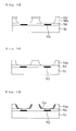
- FIG. 6 is a flowchart illustrating a method of manufacturing a plasma display panel according to a first preferred embodiment of the present invention
- FIGS. 7A to 7J are views illustrating the method of manufacturing a plasma display panel according to the first preferred embodiment of the present invention.
- a method of manufacturing a plasma display panel includes the steps of preparing material for the partitions containing inorganic powder, vehicles, and inorganic ion exchangers (S610) and forming the partitions in a lower plate using the material for the partitions (S620 to S640).
- the inorganic powder has a weight ratio of 60% to 80%
- the vehicles have a weight ratio of 20% to 40%
- the inorganic ion exchangers have a weight ratio of 0.01% to 5%, and more preferably, 0.1% to 5%.
- the components and compositions of the inorganic powder, the vehicles, and the inorganic ion exchangers are identical to those of the material for the partitions of the plasma display panel as described above.
- a rear glass 711 is prepared, and preferably, the rear glass 711 is a soda-lime glass or PD200.
- an address electrode 713 is formed, and as shown in FIG. 7C, a lower dielectric material layer 715 is formed to cover the rear glass 711 and the address electrode 713.
- partition 712a is formed on the lower dielectric material layer 715.
- the material for the partition 712a is coated on the lower dielectric material layer 715 (S620).
- the coating of the material for the partition 712a is carried out by printing the material for the partition in the form of paste or laminating a partition green sheet in the form of slurry.
- the components and compositions of the material for the partition are identical to the components and compositions of the material for the partition of the plasma display panel as described above.
- the coated material for the partition 712a is exposed by lithography to develop (S630), the lithography includes the steps of coating photo resist 730 on the material for the partition 712a as shown in FIG.
- the photo resist 730 is removed and baked to complete the partition 712a (S640).
- the baking temperature is preferably 500 degrees centigrade to 600 degrees centigrade, and more preferably, 540 degrees centigrade to 560 degrees centigrade.
- the method as described above is described as a method of coating the material for the partition and projecting light to the material for the partition to expose the material for the partition.
- a photosensitive initiator is contained in the material for the partition
- the photo mask is covered and exposed to the light without using the photo resist and the portion which is not exposed to the light is removed by the developing solution.
- the photo resist is exposed to the light and developed and the portion in which the photo resist does not remain is removed by sanding.
- the photo resist is exposed to the light and developed and etching liquid is sprayed to remove the portion in which the photo resist does not remain.
- phosphor 714 is coated on the upper side of the lower dielectric material layer 715 and on a side of the partition 712a to complete the lower substrate.
- the substrate manufactured by the above-described process is bonded to the front substrate having the address electrode using sealing material such as seal frit, and in more detail, the seal frit is baked and heated to discharge impurities existing in the seal frit.
- inert gas such as helium gas He, Neon gas Ne, Xenon gas Xe, or the like is injected.
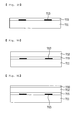
- FIG. 8 is a flowchart illustrating a method of manufacturing a plasma display panel according to a second preferred embodiment of the present invention
- FIGS. 9A to 9K are views illustrating the method of manufacturing a plasma display panel according to the second preferred embodiment of the present invention.
- the method according to this preferred embodiment of the present invention is different from the method according to the first preferred embodiment of the present invention in view of forming the partition having the same composition as the composition of the conventional partition (S810) and forming a separate partition protective layer (S820 to S840).
- FIGS. 9A to 9I on the lower glass 711, address electrodes 713 and a dielectric material layer 751 are formed, material for partitions is coated, the exposure process is carried out, and the developing process is carried out to form partitions 712.
- the components and the compositions of the material for the partitions are identical to those of the conventional material for the partitions.
- Material for a partition protective layer is prepared (S820), as shown in FIG. 9J, the material for the partition protective layer is coated on the partitions (S830) and is baked (S840), and phosphor 814 is coated as shown in FIG. 9K to complete a rear substrate.
- the material for the partition protective layer includes a solvent, binders, dispersant, and inorganic ion exchangers, and details of components and compositions thereof are identical to those of the material for the partition protect layer of the plasma display panel as described above, and preferably, is coated by a spray method.
- baking temperature is 500 degrees centigrade to 600 degrees centigrade, and more preferably, 540 degrees centigrade to 560 degrees centigrade.
- the rear substrate manufactured by the above-described process is bonded to the front substrate and inert gas such as helium gas He, Neon gas Ne, Xenon gas Xe, or the like is injected thereinto to complete the plasma display panel.
- inert gas such as helium gas He, Neon gas Ne, Xenon gas Xe, or the like is injected thereinto to complete the plasma display panel.
- the inorganic ion exchangers are added to the partitions or the surfaces of the partitions.
- the inorganic ion exchangers capture Na + so that the quantity of Na + reacting with Ag + is reduced.
- the quantity of Ag + reduced into Ag 0 decreases to prevent the yellow discoloration so that color temperature of the white ray of the plasma display panel may be improved and light permeability may be also improved.
- the yellow discoloration is prevented so that optical characteristics and external appearance of the plasma display panel may be enhanced.
- the content of Na of the soda-lime glass is very high, about three times PD200, thereby causing the yellow discoloration to be significantly generated, it is preferred to use the inorganic ion exchangers.
Landscapes
- Engineering & Computer Science (AREA)
- Physics & Mathematics (AREA)
- Plasma & Fusion (AREA)
- Manufacturing & Machinery (AREA)
- Gas-Filled Discharge Tubes (AREA)
Applications Claiming Priority (1)
| Application Number | Priority Date | Filing Date | Title |
|---|---|---|---|
| KR1020050036031A KR20060113137A (ko) | 2005-04-29 | 2005-04-29 | 플라즈마 디스플레이 패널 및 그 제조방법 |
Publications (2)
| Publication Number | Publication Date |
|---|---|
| EP1720190A2 true EP1720190A2 (fr) | 2006-11-08 |
| EP1720190A3 EP1720190A3 (fr) | 2009-11-11 |
Family
ID=36997915
Family Applications (1)
| Application Number | Title | Priority Date | Filing Date |
|---|---|---|---|
| EP06290676A Withdrawn EP1720190A3 (fr) | 2005-04-29 | 2006-04-26 | Ecran plasma, sa méthode de fabrication et la composition de ses parois séparatrices |
Country Status (5)
| Country | Link |
|---|---|
| US (1) | US20060244379A1 (fr) |
| EP (1) | EP1720190A3 (fr) |
| JP (1) | JP2006310318A (fr) |
| KR (1) | KR20060113137A (fr) |
| CN (1) | CN1877777A (fr) |
Families Citing this family (6)
| Publication number | Priority date | Publication date | Assignee | Title |
|---|---|---|---|---|
| TWI624890B (zh) | 2013-08-22 | 2018-05-21 | 櫻花彩色筆股份有限公司 | Indicator for electronic component manufacturing apparatus, and design and/or management method of the same |
| WO2015122425A1 (fr) | 2014-02-14 | 2015-08-20 | 株式会社サクラクレパス | Indicateur de détection de traitement par plasma |
| JP2015205995A (ja) | 2014-04-21 | 2015-11-19 | 株式会社サクラクレパス | プラズマ処理検知用インキ組成物及びプラズマ処理検知インジケータ |
| JP6474390B2 (ja) | 2014-05-09 | 2019-02-27 | 株式会社サクラクレパス | 変色層として無機物質を使用したプラズマ処理検知インジケータ |
| JP6567863B2 (ja) | 2014-09-16 | 2019-08-28 | 株式会社サクラクレパス | プラズマ処理検知用インキ組成物及びプラズマ処理検知インジケータ |
| JP6567817B2 (ja) | 2014-12-02 | 2019-08-28 | 株式会社サクラクレパス | プラズマ処理検知インキ組成物及びそれを用いたプラズマ処理検知インジケータ |
Family Cites Families (14)
| Publication number | Priority date | Publication date | Assignee | Title |
|---|---|---|---|---|
| JPS59170173A (ja) * | 1983-03-18 | 1984-09-26 | Toagosei Chem Ind Co Ltd | 封着剤 |
| US4598037A (en) * | 1984-12-21 | 1986-07-01 | E. I. Du Pont De Nemours And Company | Photosensitive conductive metal composition |
| JPH09132652A (ja) * | 1995-11-09 | 1997-05-20 | Asahi Shiyueebell Kk | 積層板 |
| JP3904097B2 (ja) * | 1997-03-03 | 2007-04-11 | 日立化成工業株式会社 | 異方導電性接続部材 |
| US6360562B1 (en) * | 1998-02-24 | 2002-03-26 | Superior Micropowders Llc | Methods for producing glass powders |
| JP2000183470A (ja) * | 1998-12-16 | 2000-06-30 | Sony Corp | マイグレーションの防止された配線およびその防止方法 |
| US6624799B1 (en) * | 1999-11-18 | 2003-09-23 | Lg Electronics Inc. | Radio frequency plasma display panel |
| JP2001236885A (ja) * | 2000-02-22 | 2001-08-31 | Matsushita Electric Ind Co Ltd | プラズマディスプレイパネルおよびその製造方法 |
| KR20010095198A (ko) * | 2000-03-31 | 2001-11-03 | 마츠시타 덴끼 산교 가부시키가이샤 | 디스플레이 패널 및 그 제조방법 |
| JP2003008236A (ja) * | 2001-06-27 | 2003-01-10 | Hitachi Chem Co Ltd | 感光性樹脂組成物、それを用いた多層プリント配線板及びビルドアップ多層配線板の製造方法 |
| WO2003003398A2 (fr) * | 2001-06-29 | 2003-01-09 | Thomson Plasma | Dalle pour panneau a plasma a barrieres poreuses renforcees |
| JP3389243B1 (ja) * | 2001-07-03 | 2003-03-24 | 松下電器産業株式会社 | プラズマディスプレイパネルおよびその製造方法 |
| KR100525888B1 (ko) * | 2003-06-23 | 2005-11-02 | 엘지전자 주식회사 | 화이트백 형성용 페이스트 조성물 및플라즈마디스플레이패널의 하판제조방법 |
| US7279837B2 (en) * | 2004-03-24 | 2007-10-09 | Samsung Sdi Co., Ltd. | Plasma display panel comprising discharge electrodes disposed within opaque upper barrier ribs |
-
2005
- 2005-04-29 KR KR1020050036031A patent/KR20060113137A/ko not_active Withdrawn
-
2006
- 2006-04-26 EP EP06290676A patent/EP1720190A3/fr not_active Withdrawn
- 2006-04-27 US US11/380,588 patent/US20060244379A1/en not_active Abandoned
- 2006-04-29 CN CNA2006100799645A patent/CN1877777A/zh active Pending
- 2006-05-01 JP JP2006127426A patent/JP2006310318A/ja not_active Withdrawn
Also Published As
| Publication number | Publication date |
|---|---|
| EP1720190A3 (fr) | 2009-11-11 |
| CN1877777A (zh) | 2006-12-13 |
| US20060244379A1 (en) | 2006-11-02 |
| JP2006310318A (ja) | 2006-11-09 |
| KR20060113137A (ko) | 2006-11-02 |
Similar Documents
| Publication | Publication Date | Title |
|---|---|---|
| JP2004241379A (ja) | プラズマディスプレイ部材およびプラズマディスプレイ、並びにプラズマディスプレイ部材の製造方法 | |
| EP1772890A2 (fr) | Procédé de préparation d'un panneau d'affichage à plasma | |
| EP1381071B1 (fr) | Dispositif d'affichage à plasma | |
| US20040046504A1 (en) | Plasma display panel and a plasma display panel production method | |
| EP1720190A2 (fr) | Ecran plasma, sa méthode de fabrication et la composition de ses parois séparatrices | |
| EP1858053A2 (fr) | Ecran plasma et son procédé de fabrication | |
| WO2003075301A1 (fr) | Ecran a plasma | |
| JP3067673B2 (ja) | カラープラズマディスプレイパネル | |
| JP2002056775A (ja) | プラズマディスプレイパネル用基板の製造方法、プラズマディスプレイパネル用基板及びプラズマディスプレイパネル | |
| WO2007094202A1 (fr) | Panneau d'affichage a plasma | |
| WO2007094239A1 (fr) | Ecran plasma | |
| JP4934665B2 (ja) | プラズマディスプレイパネル | |
| JP4195997B2 (ja) | プラズマディスプレイパネルおよびその製造方法 | |
| JP2002367518A (ja) | プラズマディスプレイパネル用電極、プラズマディスプレイパネル | |
| KR20080085522A (ko) | 감광성 격벽 재료, 그 제조방법 및 이를 이용한 플라즈마디스플레이 패널의 제조방법 | |
| JP4389684B2 (ja) | プラズマディスプレイパネル | |
| JPH0971403A (ja) | ガス放電型表示パネル用誘電体材料、誘電体材料組成物 | |
| EP1677333A1 (fr) | Plaque verte, écran à plasma et procédé de fabrication d'écran à plasma | |
| JP2008108719A (ja) | プラズマディスプレイ用部材の製造方法 | |
| KR100728211B1 (ko) | 플라즈마 디스플레이 패널 및 그 제조 방법 | |
| US20080036380A1 (en) | Plasma display panel and method of manufacturing the same | |
| JP4259190B2 (ja) | プラズマディスプレイパネルの製造方法 | |
| JPH1116503A (ja) | プラズマディスプレイパネルの隔壁及び蛍光体形成用積層シート | |
| KR100739573B1 (ko) | 플라즈마 디스플레이 패널의 제조 방법 | |
| JP2005135831A (ja) | プラズマディスプレイパネル |
Legal Events
| Date | Code | Title | Description |
|---|---|---|---|
| PUAI | Public reference made under article 153(3) epc to a published international application that has entered the european phase |
Free format text: ORIGINAL CODE: 0009012 |
|
| AK | Designated contracting states |
Kind code of ref document: A2 Designated state(s): AT BE BG CH CY CZ DE DK EE ES FI FR GB GR HU IE IS IT LI LT LU LV MC NL PL PT RO SE SI SK TR |
|
| AX | Request for extension of the european patent |
Extension state: AL BA HR MK YU |
|
| PUAL | Search report despatched |
Free format text: ORIGINAL CODE: 0009013 |
|
| AK | Designated contracting states |
Kind code of ref document: A3 Designated state(s): AT BE BG CH CY CZ DE DK EE ES FI FR GB GR HU IE IS IT LI LT LU LV MC NL PL PT RO SE SI SK TR |
|
| AX | Request for extension of the european patent |
Extension state: AL BA HR MK YU |
|
| AKX | Designation fees paid | ||
| REG | Reference to a national code |
Ref country code: DE Ref legal event code: 8566 |
|
| STAA | Information on the status of an ep patent application or granted ep patent |
Free format text: STATUS: THE APPLICATION IS DEEMED TO BE WITHDRAWN |
|
| 18D | Application deemed to be withdrawn |
Effective date: 20100512 |