EP1720215A1 - Circuit de traitement du signal, carte sans contact IC et étiquette utilisant ce circuit - Google Patents
Circuit de traitement du signal, carte sans contact IC et étiquette utilisant ce circuit Download PDFInfo
- Publication number
- EP1720215A1 EP1720215A1 EP06008824A EP06008824A EP1720215A1 EP 1720215 A1 EP1720215 A1 EP 1720215A1 EP 06008824 A EP06008824 A EP 06008824A EP 06008824 A EP06008824 A EP 06008824A EP 1720215 A1 EP1720215 A1 EP 1720215A1
- Authority
- EP
- European Patent Office
- Prior art keywords
- frequency
- carrier
- signal processing
- conductor lines
- processing circuit
- Prior art date
- Legal status (The legal status is an assumption and is not a legal conclusion. Google has not performed a legal analysis and makes no representation as to the accuracy of the status listed.)
- Granted
Links
- 239000004020 conductor Substances 0.000 claims description 94
- 239000000463 material Substances 0.000 claims description 23
- 239000000969 carrier Substances 0.000 claims description 4
- 230000000903 blocking effect Effects 0.000 claims 4
- 230000005540 biological transmission Effects 0.000 abstract description 18
- 230000005684 electric field Effects 0.000 description 12
- 238000004891 communication Methods 0.000 description 11
- 238000010586 diagram Methods 0.000 description 7
- 229920000139 polyethylene terephthalate Polymers 0.000 description 4
- 239000005020 polyethylene terephthalate Substances 0.000 description 4
- 238000010897 surface acoustic wave method Methods 0.000 description 4
- 230000001939 inductive effect Effects 0.000 description 3
- 229920005989 resin Polymers 0.000 description 3
- 239000011347 resin Substances 0.000 description 3
- 238000004804 winding Methods 0.000 description 3
- 230000004888 barrier function Effects 0.000 description 2
- 239000003822 epoxy resin Substances 0.000 description 2
- 230000008676 import Effects 0.000 description 2
- 238000012986 modification Methods 0.000 description 2
- 230000004048 modification Effects 0.000 description 2
- 229920000647 polyepoxide Polymers 0.000 description 2
- -1 polyethylene terephthalate Polymers 0.000 description 2
- 230000005855 radiation Effects 0.000 description 2
- 230000001105 regulatory effect Effects 0.000 description 2
- 239000000758 substrate Substances 0.000 description 2
- 206010016275 Fear Diseases 0.000 description 1
- 229910003327 LiNbO3 Inorganic materials 0.000 description 1
- 239000000853 adhesive Substances 0.000 description 1
- 230000001070 adhesive effect Effects 0.000 description 1
- 239000003990 capacitor Substances 0.000 description 1
- 230000009977 dual effect Effects 0.000 description 1
- 230000008030 elimination Effects 0.000 description 1
- 238000003379 elimination reaction Methods 0.000 description 1
- GQYHUHYESMUTHG-UHFFFAOYSA-N lithium niobate Chemical compound [Li+].[O-][Nb](=O)=O GQYHUHYESMUTHG-UHFFFAOYSA-N 0.000 description 1
- 238000004519 manufacturing process Methods 0.000 description 1
- 230000008520 organization Effects 0.000 description 1
- 230000001681 protective effect Effects 0.000 description 1
- 230000009467 reduction Effects 0.000 description 1
Images


Classifications
-
- H—ELECTRICITY
- H01—ELECTRIC ELEMENTS
- H01Q—ANTENNAS, i.e. RADIO AERIALS
- H01Q9/00—Electrically-short antennas having dimensions not more than twice the operating wavelength and consisting of conductive active radiating elements
- H01Q9/04—Resonant antennas
- H01Q9/16—Resonant antennas with feed intermediate between the extremities of the antenna, e.g. centre-fed dipole
- H01Q9/28—Conical, cylindrical, cage, strip, gauze, or like elements having an extended radiating surface; Elements comprising two conical surfaces having collinear axes and adjacent apices and fed by two-conductor transmission lines
- H01Q9/285—Planar dipole
-
- H—ELECTRICITY
- H01—ELECTRIC ELEMENTS
- H01Q—ANTENNAS, i.e. RADIO AERIALS
- H01Q1/00—Details of, or arrangements associated with, antennas
- H01Q1/12—Supports; Mounting means
- H01Q1/22—Supports; Mounting means by structural association with other equipment or articles
-
- H—ELECTRICITY
- H01—ELECTRIC ELEMENTS
- H01Q—ANTENNAS, i.e. RADIO AERIALS
- H01Q9/00—Electrically-short antennas having dimensions not more than twice the operating wavelength and consisting of conductive active radiating elements
- H01Q9/04—Resonant antennas
- H01Q9/16—Resonant antennas with feed intermediate between the extremities of the antenna, e.g. centre-fed dipole
- H01Q9/26—Resonant antennas with feed intermediate between the extremities of the antenna, e.g. centre-fed dipole with folded element or elements, the folded parts being spaced apart a small fraction of operating wavelength
- H01Q9/27—Spiral antennas
Definitions
- the present invention relates to a signal processing circuit provided on a non-contact IC card or tag such as a cash card, credit card, commutation ticket, coupon ticket, management card, In card, driver's license, commodity management tag, and logistic management card used in a cash dispenser, electronic money system, automatic ticket gate, entry/exit management system, commodity management system, and logistic management system, and to a signal processing circuit equipped with an antenna used for transmission of an operating power and communication between the non-contact IC card or tag and a reader/writer.
- a signal processing circuit provided on a non-contact IC card or tag such as a cash card, credit card, commutation ticket, coupon ticket, management card, In card, driver's license, commodity management tag, and logistic management card used in a cash dispenser, electronic money system, automatic ticket gate, entry/exit management system, commodity management system, and logistic management system, and to a signal processing circuit equipped with an antenna used for transmission of an operating power and communication between the non-contact IC card or tag and a reader/writer.
- the non-contact IC card or tag mainly uses electromagnetic waves of High Frequency (HF) to Ultra High Frequency (UHF) bands to perform power transmission and communication.
- HF High Frequency
- UHF Ultra High Frequency
- the HF band is known as a frequency band of 3 MHz to 30 MHz, among other things, the use of carrier of 13.56 MHz is prevailing for communication and power transmission between a non-contact IC card or tag (hereinafter, collectively referred to as "Radio Frequency Identification" RFID) and a reader/writer.
- the UHF band is generally known as a frequency band of 300 MHz to 3000 MHz.
- a carrier of 2.45 GHz is available in Japan and a frequency band of 860 MHz to 960 MHz is available in the United States and Europe for communication and power transmission between the RFID and reader/writer.
- a frequency of 5.8 GHz higher than the above band is allowed to be used in one-way communication from the RFID to a reader in a toll load.
- Transmission and reception of electric power and information by the carrier of the HF band between the RFID and reader/writer is mainly performed in such a manner that a spiral antenna provided on the RFID is interlinked with magnetic field outputted from the antenna of the reader/writer to cause the spiral antenna to induce an electric power and signal current.
- the supply of electric power to RFID and the transmission and reception of information by the carrier of the UHF band are mainly performed in such a manner that a dipole antenna or a patch antenna provided on the RFID receives electric field from a reader/writer and the like to induce an electric power and signal current.
- patent document 1 has proposed a hybrid-type IC card on which a near magnetic field-type module using the carrier of the HF band and a radio-type module using the carrier of the UHF band are mounted.
- a non-contact IC card similar to the above has been disclosed in the following patent document 2 and a communication terminal device similar to the above is also disclosed in the following patent document 3.
- the non-contact IC card or tag for a system using both the HF and UHF bands has hitherto adapted to mount antennas responding to the respective frequencies and corresponding to the number of the carrier frequencies. This widens a mounting area of the non-contact IC card and tag, and an IC to be mounted thereon increases in chip size because of the need for terminals for each of the antennas.
- an antenna usable in a plurality of bands enables reducing a mounting area and a chip size. It is also expected that interference occurred between the antennas can be suppressed.
- the present invention has for its purpose to provide a single antenna capable of responding to a plurality of usable bands.
- a spiral antenna being used in the HF band and inducing voltage by magnetic field is greatly different from a dipole antenna being used in the UHF band and inducing voltage by electric field in that in the former one end of a conductor (wiring) composing the antenna is structurally short-circuited to the other end thereof, but in the latter it is structurally open-circuited.
- An antenna for effectively transmitting and receiving a signal and electric power in both the HF and UHF bands needs selecting either of the above structures. Inventor's attention has been drawn by "folded dipole antenna" which induces an electric field in the UHF band and one and the other end of which are short-circuited.
- An antenna of this type is so structured that both open ends of the dipole are folded and short-circuited with another path. For this reason, a current being reverse in phase to the original dipole part (portion not to be folded) is distributed on a line composing a folded dipole-type antenna, but the directions of currents to be produced on the lines to be folded and not to be folded are opposite, so that the electric field to be radiated will be in phase.
- the inventor has attempted to extend the distance of the dipole structure between a part extending from the end thereof (part to which elements such as ICs are electrically connected) to the primary direction (i.e., a part not to be folded) and a part extending opposite to the primary direction (i.e. , part to be folded) to shape the folded dipole structure into a loop.
- current waveforms alternating current waveforms according to the frequency of a carrier
- the above folded dipole-type antenna is formed as a loop antenna whose line length is sufficiently shorter than the carrier wavelength of the HF band and functions as a folded dipole antenna which is slightly lower in transmission and reception efficiency for the carrier of the UHF band, which enables a single antenna to realize effective transmission and reception in two frequency bands.
- the folded dipole structure into a spiral shape because the antenna for transmitting and receiving the carrier of the HF band requires some inductive components. Then, a plurality of conductor lines (antenna elements) with the folded dipole structure are connected in series to produce a spiral antenna composed of multi-stage antenna elements.
- the antenna element positioned at the outer periphery is different in length per turn from that at the inner periphery.
- the present invention provides a signal processing circuit being included in a non-contact IC card or tag (RFID) and capable of acting to transmit an electric power and communicate between the RFID and the external device such as a reader/writer, the signal processing circuit on which a rectangular spiral antenna is provided, thereby performing communication by using at least two carrier frequencies.
- the signal processing circuit is provided with ICs including an RF circuit or circuit element responding to each of the two carrier frequencies and supplied by power from the external device through the above rectangular spiral antenna, or performs transmission and reception of information with the external device.
- the rectangular spiral antenna is structured by sequentially arranging (for example, coaxially) a plurality of the conductor lines with the folded dipole structure from the outer toward the inner periphery thereof.
- the line length of the rectangular spiral antenna satisfies the relationship of L ⁇ ⁇ 1 in terms of using the rectangular spiral antenna as a loop antenna, of transmitting an electric power to the signal processing circuit by the carrier with a wavelength of ⁇ 1 and of transmitting and receiving information.
- the conductor lines sequentially extend from one end positioned at the first long side to the other end positioned at the first long side via the first long side, the second short side, the second long side and the second short side.
- the other end of one of the conductor lines is connected to one end of the other of the conductor line at the first long side to draw a spiral line.
- the total length (for example, sum of lengths of N conductor lines composing the rectangular spiral antenna) will be a line length L of the rectangular spiral antenna.
- a single antenna adapted to at least two usable frequency bands, relative to conventional RFID systems makes a non-contact 1C card and tag adaptable to a variety of systems, small and inexpensive.
- Fig. 1 shows an antenna 101 according to the present invention characterized by being available in two frequency bands.
- the antenna is spiral and has again effective in two carrier frequency bands.
- the two carrier frequencies are taken as f 1 and f 2 (f 1 ⁇ f 2 )
- the relation of wavelengths ⁇ 1 and ⁇ 2 ( ⁇ 1 > ⁇ 2 ) corresponding to the carrier frequencies to the line length L and the number of windings N of the antenna (N is an integer of two or more) is expressed by the following formulas: L ⁇ ⁇ ⁇ 1 L ⁇ N ⁇ 2
- the line length of the antenna is much shorter than the wavelength of the carrier as expressed in the formula (1), so that a current distribution 110 above the antenna line becomes substantially uniform as shown in Fig. 2.
- a current 111 flows along a wiring (conductor line) composing the antenna 101, thereby generating magnetic field H (line of magnetic force 112) from an opening formed by the loop of the antenna 101.
- mutual inductance generated between a spiral antenna provided on a reader/writer (R/W, not shown) and the antenna 101 performs the transmission of electric power and the transfer of communication signals.
- the length of the spiral antenna 101 per turn is approximately equal to the wavelength as expressed in the formula (2), so that a current distribution 113 above the antenna line reverses in phase on the way as shown in Fig. 3.
- Providing an integrated circuit (IC) 102 around the center in the longitudinal direction of the antenna causes the above current distribution to indicate a positive phase 113a on one side in the longitudinal direction and a negative phase 113b on the other side.
- IC integrated circuit
- a current waveform 113 is compared to a sinusoidal wave, it is shown that waveforms crossing over from the first to the second quadrant and from the third to the fourth quadrant appear on one side and on the other side in the longitudinal direction respectively, and both the waveforms are reverse to each other in phase.
- the current distribution 113a with a positive phase generates an electric field E (hereinafter, electric line of force 114 is read as electric field) in the tangential direction of the current direction, but the current distribution 113b with a negative phase generates an electric field 114 in the tangential direction opposite to the current direction.
- the direction in which the current 111 generating these electric fields 114 or induced by the electric fields 114 flows along a wiring (conductor line) is opposite from one side to the other in the longitudinal direction, so that the electric fields 114 produced at the respective sides are same in phase with each other and are strengthened with each other.
- This provides the spiral antenna 101 with a gain effective for a dipole antenna. That is basically produced as is the case with a folded dipole antenna.
- a length 105 of long side of the wiring (conductor line) at the outermost periphery (the outer dimension in the longitudinal direction of the antenna) is taken as L xo
- a length 103 of short side is taken as L yo
- a distance 107 between a pair of the adjacent conductor lines (pitch between the antenna wirings) is taken as "p" in any of the longitudinal and the widthwise direction.
- the rectangular spiral antenna 101 When the rectangular spiral antenna 101 functions as a dipole antenna, it receives and transmits a carrier with a wavelength ⁇ at the long side.
- the long side of the rectangular spiral antenna 101 is shorter than ⁇ /2 even at the conductor line at the outermost periphery where it is the longest.
- the part will not contribute as a dipole antenna to the radiation of a carrier. Shifting more than that lowers a radiation efficiency. For this reason, the current distribution 113 at the conductor line composing the rectangular.spiral antenna 101 is reversed in phase at the part extending toward the short side.
- the rectangular spiral antenna 101 as a dipole antenna receives and transmits a carrier with a wavelength ⁇ at the long side.
- the number of windings N of the rectangular spiral antenna 101 and a pitch for each turn satisfies the formula (3) as in the case (B). It is also desirable that the length of the long side of the other conductor line adjacent to the conductor line at the innermost periphery (the conductor line located at the first turn from the innermost periphery) is shorter than ⁇ /2.
- the feeding point may be provided at the midpoint in the longitudinal direction of the rectangular spiral antenna (for example, the outer dimension in the longitudinal direction of the antenna: L xo shown in Fig. 1), or may be slightly shifted from the midpoint to the longitudinal direction.
- a value dx of a shift 109 at a position where IC is mounted (feeding point) with respect to the center (midpoint) in the longitudinal direction of the rectangular spiral antenna has tobe kept within range of for example " ⁇ 8np
- n 1 to N .”
- the value can be approximately specified as "(N - 1) ⁇ 8p" or less.
- the feeding point lies at a position where the conductor line at the outermost periphery is terminated at one side thereof extending in its longitudinal direction (or in the vicinity), so that the position influences current waveforms produced in the longitudinal directionof the conductor line.
- setting the position of the feeding point at the midpoint in the longitudinal direction or within range of a predetermined distance away from that position suppresses the influence on the current waveforms to a negligible extent.
- "Within range of a predetermined distance" stated above means a range of which upper limit is the maximum value of "shift in positions between the conductor lines at the outermost and the innermost periphery.”
- the inner dimension in the longitudinal direction of the antenna L xi is shorter than ⁇ /2 in terms of preventing current from reversing in phase in the longitudinal direction of the rectangular spiral antenna.
- the signal processing circuit is equipped with IC including an RF circuit and the rectangular spiral antenna being a planar coil, particularly characterized in that communication is performed using at least two carrier frequencies by means of the rectangular spiral antenna.
- one of the two carrier frequencies is in the HF band (in general, a frequency band of 3 MHz to 30 MHz, 13.56 MHz is prevailing) and the other in the UHF band (in general, a frequency band of 300 MHz to 3000 MHz, including 5.8 GHz exceptionally).
- the latter is 100 times higher than the former in carrier frequency.
- the rectangular spiral antenna 101 as a loop antenna supplies electric power from the external device to an integrated circuit (IC) 102 provided in the signal processing circuit by the carrier of the HF band (hereinafter referred to as "carrier of a first frequency") to import information and sends information from IC 102 to the external device.
- the rectangular spiral antenna 101 as a dipole antenna supplies electric power from the external device to an integrated circuit (IC) 102 provided in the signal processing circuit by the carrier of the UHF band (hereinafter referred to as "carrier of a second frequency") to import information and send information from IC 102 to the external device.
- the wavelength corresponding thereto is about 22 m.
- the second frequency is set at a frequency band of 860 MHz to 960 MHz, the wavelength ranges from 30 cm to 35 cm. If it is set at 2.45 GHz, the wavelength is about 12 cm.
- the line length L of the rectangular spiral antenna 101 is 165 cm, which is shorter than that of the first frequency. If the long side of the conductor line positioned at the outermost periphery of the rectangular spiral antenna 101 is 12.5 cm and the short side is 4.5 cm, the current corresponding to the wavelength (about 35 cm) of the second frequency shorter than that of the first frequency is less liable to reverse in phase at the long side.
- the rectangular spiral antenna 101 can be further downsized and be contained in a credit card.
- Fig. 4 shows a schematic diagram of a credit card formed as non-contact IC card 200 provided with a signal processing circuit for receiving the carrier of the first frequency of 13.56 MHz and the carrier of the second frequency of 2.45 GHz.
- the rectangular spiral antenna 101 is formed by connecting in series three conductor lines 1a to 1c of which both ends (a first and a second end) are positioned the first side and the other end (the second end) of both the ends is positioned at a inner side than the one thereof (the first end).
- Each of the conductor lines 1a to 1c extends from the first end thereof through the second, third and fourth sides of the above rectangular spiral antenna 101 in that order, returns to the first side and terminates at the second end thereof.
- the first end of the conductor line 1a at the outermost periphery is one of the feeding points 121 connected to ICs (102a and 102b).
- the second end thereof is connected to the first end of the conductor line 1b adjacent to the conductor line 1a.
- the second end of the conductor line 1b positioned at the first turn from the outer periphery is connected to the first end of the conductor line 1c adjacent to the conductor line 1b.
- the second end of the conductor line 1c at the innermost periphery is the other one of the above feeding points 121.
- These conductor lines 1a to 1c are collectively printed on a resin substrate that is a base material 201 for the non-contact IC card.
- a resin film on which the conductor lines 1a to 1c are printed may be stuck on the principal plane of the base material 201.
- integrated circuit elements mounted thereon are divided into a first integrated circuit 102a responding to the first frequency and a second integrated circuit 102b responding to the second frequency, instead of applying a hybrid type responding each of the carriers of the first and the second frequency as shown in Fig. 1.
- a branch circuit 120 is provided between the feeding point 121 and the first and second integrated circuits 102a and 102b to prevent the second integrated circuit 102b from malfunctioning due to the carrier of the first frequency and the first integrated circuit 102a from malfunctioning due to the carrier of the second frequency.
- Fig. 4 (b) is a schematic-diagram showing one example of the branch circuit 120.
- the branch circuit 120 is formed as a resonator using two surface acoustic wave (SAW) devices in which comb-shaped electrodes 123a to 123c and 124a to 124c are formed on the principal plane of the base material 130 composed of piezo material such as lithium niobate (LiNbO 3 ).
- the input electrodes 123a and 124a of the branch circuit are connected to a feeder 122 extending from a feeding point 7.21a connected to the conductor line 1a and from a feeding point 121b connected to the conductor line 1c.
- the SAW resonator provided with the comb-shaped electrodes 123a to 123c functions' as a band pass filter (low pass filter) 123 which passes a signal of the first frequency to the output electrode 123b but does not pass that of the second frequency.
- the SAW resonator provided with the comb-shaped electrodes 124a to 124c functions as a band pass filter (high pass filter) 124 which passes a signal of the second frequency to the output electrode 124b but does not pass that of the first frequency.
- the space between the comb-shaped electrodes 124a to 124c provided on the band pass filter 124 is narrower than that between the comb-shaped electrodes 123a to 123c provided on the band pass filter 123 according to the wavelength of the signal to be passed.
- the output electrode 123b of the band pass filter 123 is connected to the first integrated circuit 102a and the output electrode 124b of the band pass filter 124 is connected to the first integrated circuit 102b.
- the rectangular spiral antenna 101 composed of the conductor lines 1a to 1c shown in Fig. 4(a) is abridged to a single conductor line 1 for convenience of drawing.
- the base material 130 on which the branch circuit 120 is formed is embedded within a recess formed in a resin substrate that is the base material 201 for the non-contact IC card.
- Two feeding points 121a and 121b illustrated by black squares are connected to the feeder 122 formed on the base material 130.
- Fig. 4(c) shows a schematic diagram of the non-contact IC card using the integrated circuit 102 into which the first and the second integrated circuit 102a and 102b shown in Fig. 4 (a) are integrated.
- the branch circuit 120 is provided between the feeding point 121 and the integrated circuit 102.
- electrodes 120a and 120b for receiving signals of the first and the second frequency respectively are provided and mounted facedown on the base material 130 to connect the electrodes 120a and 120b to the output electrode 123b of the band pass filter 123 and the output electrode 124b of the band pass filter 124 respectively.
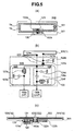
- Fig. 5 (a) shows a schematic diagram of a tag (IC tag) with a signal processing circuit for receiving the carrier of the first frequency of 13.56 MHz and the carrier of the second frequency of 900 MHz.
- the tag is formed on a flexible base material 301 composed of epoxy resin or polyethylene terephthalate (PET) so that it can be pasted on delivery such as a parcel.
- the rectangular spiral antenna 101 is printed for example on the principal plane of the base material 301.
- the rectangular spiral antenna 101, of which two conductor lines 1a and 1b are connected in series to each other, is so formed to meet the following; the outer dimension in the longitudinal direction of the antenna (length L xo shown in Fig.
- the antenna wiring width 108 (refer to Fig. 1, the width w of the conductor line) is narrowed like a microstrip line. This however does not hinder transmission and reception of the carrier of the first frequency with a wavelength of 22.1 m unless the number of the conductor lines N is 44 or more.
- the tag shown in Fig. 5(a) are mounted the first and second integrated circuit 102a and 102b responding to the first and the second frequency respectively as is the case with the non-contact IC card shown in Fig. 4(a).
- a branch circuit formed on the base material 130 is provided between the integrated circuits 102a and 102b and the feeding point 121 provided on both the ends of the rectangular spiral antenna 101.
- Fig. 5(b) shows one example of the branch circuit 120 provided on the tag illustrated in Fig. 5(a).
- Fig. 5(c) shows a cross section of the tag and a part of the branch circuit 120.
- the rectangular spiral antenna 101 composed of the conductor lines 1a to 1b shown in Fig. 5(a) is drawn as a single conductor line 1.
- the symbol for ground potential shown in Fig. 5(b) signifies "reference potential" in the tag circuit, the elements connected to the symbol in the figure do not need grounding.
- the feeder 122 extending the feeding point 121b provided on the other end of the innermost periphery is provided with a Schottky barrier diode 122a and a capacitor 122b.
- the Schottky barrierdiode 122a functions to demodulate signals to be received by the tag and to modulate signals to be transmitted therefrom.
- the branch circuit 120 shown in Fig. 5 (b) is provided with a bandpass filter 123 connected to the first integrated circuit 102a responding to the first frequency and a band pass filter 124 connected to the second integrated circuit 102b responding to the second frequency.
- the band pass filter 123 is equipped with a resonance circuit with an inductance 123d and a capacitance 123e, and functions as a low pass filter which passes a signal of the first frequency and blocks a signal of the second frequency.
- the band pass filter 124 is equipped with a resonance circuit with capacitances 124d and 124e and an inductance 124f, and functions as a high pass filter which passes a signal of the second frequency and blocks a signal of the first frequency.
- a conductive layer composing the inductances 123d and 124f and capacitances 123e, 124d and 124e in the branch circuit 120 is formed on the base material 7.30 like the inductance 123d shown in Fig. 5(c).
- the base material 130 can be formed by film such as epoxy resin or polyethylene terephthalate (PET) to make the tag more flexible as is the case with the base material 301 for the tag, or may be formed by film made of more flexible material.
- the inductance 123d shown in Fig. 5(c) is formed into the shape of a coil by electrically connecting conductive layers 131 (darkened in the figure) printed on both the principal planes of the base material 130 to each other via through holes formed in the base material 130.
- One of the conductive layers 131 is electrically connected to an electrode (pad) 126 formed on the first integrated circuit 102a to form a signal path between the band pass filter 123 and the first integrated circuit 102a.
- electrodes 126 on the first integrated circuit 102a shown in a blank square shows a dummy pad which does not contribute to transmission and reception of signals between the integrated circuit and the branch circuit 120.
- a conductive layer composing the capacitance 122b provided on the feeder 122 is also formed, and on one of the principal planes of the base material 130 (side opposite to the surface joined to the base material 301) is mounted the Schottky barrier diode 122a.
- the feeders 122 extending from the feeding points 121a and 121b are formed as through holes passing through the base materials 301 and 130.
- the principal plane of the base material 301 on which the rectangular spiral antenna 101 is formed is covered with a protective film 302, on the top face of which an adhesive (not shown) is coated for pasting the tag on a parcel and the like.
- any of the signal processing circuit, the non-contact IC cardand tag (RFID) with the use thereof accordingtoanembodiment of the present invention described above is capable of transmitting and receiving a plurality of carriers different in frequency band from each other by a single antenna equipped therewith, which facilitates downsizing and reducing a production cost. Elimination of need for providing a plurality of antennas in one circuit (device) dismisses fears for interference between antennas. For this reason, an RFID system being constructed by using both the HF band of which the upper output limit is regulated and the UHF band of which output may be increased can be realized by an RFID equipped with a single antenna. That is to say, the system can be practically applied without the system user's having a plurality of RFIDs (the non-contact IC card and/or tag) and without producing a new RFID including a plurality of the antennas.
Landscapes
- Details Of Aerials (AREA)
- Near-Field Transmission Systems (AREA)
- Credit Cards Or The Like (AREA)
Applications Claiming Priority (1)
| Application Number | Priority Date | Filing Date | Title |
|---|---|---|---|
| JP2005130733A JP4529786B2 (ja) | 2005-04-28 | 2005-04-28 | 信号処理回路、及びこれを用いた非接触icカード並びにタグ |
Publications (2)
| Publication Number | Publication Date |
|---|---|
| EP1720215A1 true EP1720215A1 (fr) | 2006-11-08 |
| EP1720215B1 EP1720215B1 (fr) | 2010-09-08 |
Family
ID=36754216
Family Applications (1)
| Application Number | Title | Priority Date | Filing Date |
|---|---|---|---|
| EP06008824A Expired - Lifetime EP1720215B1 (fr) | 2005-04-28 | 2006-04-27 | Circuit de traitement du signal, carte sans contact IC et étiquette utilisant ce circuit |
Country Status (5)
| Country | Link |
|---|---|
| US (1) | US7439933B2 (fr) |
| EP (1) | EP1720215B1 (fr) |
| JP (1) | JP4529786B2 (fr) |
| CN (1) | CN100433056C (fr) |
| DE (1) | DE602006016670D1 (fr) |
Cited By (1)
| Publication number | Priority date | Publication date | Assignee | Title |
|---|---|---|---|---|
| CN103107416A (zh) * | 2011-11-15 | 2013-05-15 | 财团法人工业技术研究院 | 射频辨识标签天线 |
Families Citing this family (106)
| Publication number | Priority date | Publication date | Assignee | Title |
|---|---|---|---|---|
| USD562810S1 (en) | 2004-03-29 | 2008-02-26 | Impinj, Inc. | Radio frequency identification tag antenna assembly |
| US7528728B2 (en) | 2004-03-29 | 2009-05-05 | Impinj Inc. | Circuits for RFID tags with multiple non-independently driven RF ports |
| US7667589B2 (en) | 2004-03-29 | 2010-02-23 | Impinj, Inc. | RFID tag uncoupling one of its antenna ports and methods |
| USD587691S1 (en) | 2004-03-29 | 2009-03-03 | Impinj, Inc. | Radio frequency identification tag antenna assembly |
| US7423539B2 (en) * | 2004-03-31 | 2008-09-09 | Impinj, Inc. | RFID tags combining signals received from multiple RF ports |
| USD586336S1 (en) | 2004-12-30 | 2009-02-10 | Impinj, Inc. | Radio frequency identification tag antenna assembly |
| US7519328B2 (en) * | 2006-01-19 | 2009-04-14 | Murata Manufacturing Co., Ltd. | Wireless IC device and component for wireless IC device |
| USD546821S1 (en) * | 2006-02-17 | 2007-07-17 | Impinj, Inc. | Radio frequency identification tag antenna assembly |
| US9064198B2 (en) | 2006-04-26 | 2015-06-23 | Murata Manufacturing Co., Ltd. | Electromagnetic-coupling-module-attached article |
| CN101467209B (zh) | 2006-06-30 | 2012-03-21 | 株式会社村田制作所 | 光盘 |
| JP4466689B2 (ja) * | 2006-08-31 | 2010-05-26 | 株式会社カシオ日立モバイルコミュニケーションズ | アンテナ及び携帯電子機器 |
| DE112007002024B4 (de) | 2006-09-26 | 2010-06-10 | Murata Mfg. Co., Ltd., Nagaokakyo-shi | Induktiv gekoppeltes Modul und Element mit induktiv gekoppeltem Modul |
| US7922961B2 (en) * | 2006-11-10 | 2011-04-12 | Rexam Healthcare Packaging Inc. | Molded plastic container having insert-molded insert and method of manufacture |
| US7850893B2 (en) | 2006-12-01 | 2010-12-14 | Rexam Healthcare Packaging Inc. | Molded plastic container and preform having insert-molded RFID tag |
| US8096479B2 (en) * | 2007-02-23 | 2012-01-17 | Newpage Wisconsin System Inc. | Multifunctional paper identification label |
| US8235299B2 (en) | 2007-07-04 | 2012-08-07 | Murata Manufacturing Co., Ltd. | Wireless IC device and component for wireless IC device |
| EP2138962B1 (fr) | 2007-04-26 | 2012-01-04 | Murata Manufacturing Co. Ltd. | Dispositif à circuit intégré sans fil |
| US8174454B2 (en) * | 2007-05-07 | 2012-05-08 | Infineon Technologies Ag | Dual-band antenna |
| EP2148449B1 (fr) | 2007-05-11 | 2012-12-12 | Murata Manufacturing Co., Ltd. | Dispositif ic sans fil |
| GB0709313D0 (en) * | 2007-05-15 | 2007-06-20 | Siemens Ag | RFID reader |
| DE102007029083B4 (de) * | 2007-06-21 | 2019-05-16 | ASTRA Gesellschaft für Asset Management mbH & Co. KG | Kartendatenträger mit Detektierplättchen |
| WO2009008296A1 (fr) | 2007-07-09 | 2009-01-15 | Murata Manufacturing Co., Ltd. | Dispositif à circuit intégré sans fil |
| JP4873079B2 (ja) | 2007-07-17 | 2012-02-08 | 株式会社村田製作所 | 無線icデバイス及び電子機器 |
| CN102915462B (zh) | 2007-07-18 | 2017-03-01 | 株式会社村田制作所 | 无线ic器件 |
| US20090021352A1 (en) * | 2007-07-18 | 2009-01-22 | Murata Manufacturing Co., Ltd. | Radio frequency ic device and electronic apparatus |
| JP5146872B2 (ja) * | 2007-07-24 | 2013-02-20 | Necアクセステクニカ株式会社 | 非接触icカード、携帯端末装置、起動制御方法、および起動制御プログラム |
| KR100928119B1 (ko) * | 2007-10-30 | 2009-11-24 | 삼성에스디아이 주식회사 | 인쇄회로 기판과 이를 이용한 이차전지 |
| US8929805B2 (en) | 2007-10-30 | 2015-01-06 | Nationz Technologies Inc. | System, method, and device for radio frequency communication |
| JP4462388B2 (ja) | 2007-12-20 | 2010-05-12 | 株式会社村田製作所 | 無線icデバイス |
| EP2207240B1 (fr) | 2007-12-26 | 2013-08-21 | Murata Manufacturing Co., Ltd. | Appareil d'antenne et dispositif ci sans fil |
| WO2009110381A1 (fr) * | 2008-03-03 | 2009-09-11 | 株式会社村田製作所 | Dispositif à ci sans fil et système de communication sans fil |
| EP2251933A4 (fr) * | 2008-03-03 | 2012-09-12 | Murata Manufacturing Co | Antenne composite |
| WO2009119548A1 (fr) * | 2008-03-26 | 2009-10-01 | 株式会社村田製作所 | Dispositif radio à circuit intégré |
| KR100978271B1 (ko) * | 2008-04-01 | 2010-08-26 | 엘에스산전 주식회사 | 내장형 안테나를 사용한 rfid 태그 및 이를 이용한rfid 시스템 |
| CN101953025A (zh) * | 2008-04-14 | 2011-01-19 | 株式会社村田制作所 | 无线ic器件、电子设备以及无线ic器件的谐振频率调整方法 |
| CN103295056B (zh) | 2008-05-21 | 2016-12-28 | 株式会社村田制作所 | 无线ic器件 |
| WO2009142068A1 (fr) * | 2008-05-22 | 2009-11-26 | 株式会社村田製作所 | Dispositif à circuit intégré sans fil et son procédé de fabrication |
| WO2009145007A1 (fr) | 2008-05-26 | 2009-12-03 | 株式会社村田製作所 | Système de dispositif à ci sans fil et procédé d'authentification de dispositif à ci sans fil |
| EP3509162A1 (fr) * | 2008-05-28 | 2019-07-10 | Murata Manufacturing Co., Ltd. | Dispositif ci sans fil et composant pour un dispositif ci sans fil |
| JP4557186B2 (ja) * | 2008-06-25 | 2010-10-06 | 株式会社村田製作所 | 無線icデバイスとその製造方法 |
| WO2010001469A1 (fr) | 2008-07-02 | 2010-01-07 | 三菱電機株式会社 | Dispositif de communication sans fil |
| JP4671001B2 (ja) * | 2008-07-04 | 2011-04-13 | 株式会社村田製作所 | 無線icデバイス |
| EP2320519B1 (fr) * | 2008-08-19 | 2017-04-12 | Murata Manufacturing Co., Ltd. | Dispositif à circuit intégré sans fil et procédé de fabrication de celui-ci |
| JP5429182B2 (ja) * | 2008-10-24 | 2014-02-26 | 株式会社村田製作所 | 無線icデバイス |
| CN102197537B (zh) * | 2008-10-29 | 2014-06-18 | 株式会社村田制作所 | 无线ic器件 |
| WO2010055945A1 (fr) * | 2008-11-17 | 2010-05-20 | 株式会社村田製作所 | Antenne et circuit intégré sans-fil |
| CN103500873B (zh) | 2009-01-09 | 2016-08-31 | 株式会社村田制作所 | 无线ic器件及无线ic模块 |
| WO2010082413A1 (fr) * | 2009-01-16 | 2010-07-22 | 株式会社村田製作所 | Dispositif haute fréquence et dispositif ci sans fil |
| CN102301528B (zh) | 2009-01-30 | 2015-01-28 | 株式会社村田制作所 | 天线及无线ic器件 |
| KR101023884B1 (ko) * | 2009-02-18 | 2011-03-22 | 삼성에스디아이 주식회사 | 배터리팩 |
| JP5282896B2 (ja) * | 2009-03-12 | 2013-09-04 | 日本電気株式会社 | アンテナ装置 |
| JP5282898B2 (ja) * | 2009-03-13 | 2013-09-04 | 日本電気株式会社 | アンテナ装置 |
| JP5510450B2 (ja) | 2009-04-14 | 2014-06-04 | 株式会社村田製作所 | 無線icデバイス |
| CN103022661B (zh) | 2009-04-21 | 2014-12-03 | 株式会社村田制作所 | 电子设备及天线装置的谐振频率设定方法 |
| CN102449846B (zh) | 2009-06-03 | 2015-02-04 | 株式会社村田制作所 | 无线ic器件及其制造方法 |
| US9004360B2 (en) * | 2009-06-10 | 2015-04-14 | Infineon Technologies Ag | Contactless communication via a plurality of interfaces |
| WO2010146944A1 (fr) | 2009-06-19 | 2010-12-23 | 株式会社村田製作所 | Dispositif sans fil à circuits intégrés et procédé de couplage d'un circuit d'alimentation électrique et de plaques rayonnantes |
| JP5182431B2 (ja) | 2009-09-28 | 2013-04-17 | 株式会社村田製作所 | 無線icデバイスおよびそれを用いた環境状態検出方法 |
| CN102577646B (zh) | 2009-09-30 | 2015-03-04 | 株式会社村田制作所 | 电路基板及其制造方法 |
| JP5304580B2 (ja) * | 2009-10-02 | 2013-10-02 | 株式会社村田製作所 | 無線icデバイス |
| JP5522177B2 (ja) | 2009-10-16 | 2014-06-18 | 株式会社村田製作所 | アンテナ及び無線icデバイス |
| WO2011052310A1 (fr) | 2009-10-27 | 2011-05-05 | 株式会社村田製作所 | Appareil d'émission/réception et lecteur d'étiquette sans fil |
| CN102549838B (zh) | 2009-11-04 | 2015-02-04 | 株式会社村田制作所 | 通信终端及信息处理系统 |
| EP2498207B1 (fr) | 2009-11-04 | 2014-12-31 | Murata Manufacturing Co., Ltd. | Étiquette à circuit radio intégré, lecteur/enregistreur, et système de traitement d'information |
| WO2011055701A1 (fr) | 2009-11-04 | 2011-05-12 | 株式会社村田製作所 | Terminal de communication et système de traitement de l'information |
| WO2011062238A1 (fr) | 2009-11-20 | 2011-05-26 | 株式会社村田製作所 | Dispositif d'antenne et terminal de communication mobile |
| WO2011077877A1 (fr) | 2009-12-24 | 2011-06-30 | 株式会社村田製作所 | Antenne et terminal portable |
| WO2011108340A1 (fr) | 2010-03-03 | 2011-09-09 | 株式会社村田製作所 | Module de communication sans fil et dispositif de communication sans fil |
| JP5403146B2 (ja) | 2010-03-03 | 2014-01-29 | 株式会社村田製作所 | 無線通信デバイス及び無線通信端末 |
| JP5477459B2 (ja) | 2010-03-12 | 2014-04-23 | 株式会社村田製作所 | 無線通信デバイス及び金属製物品 |
| JP5370581B2 (ja) * | 2010-03-24 | 2013-12-18 | 株式会社村田製作所 | Rfidシステム |
| WO2011122163A1 (fr) | 2010-03-31 | 2011-10-06 | 株式会社村田製作所 | Antenne et dispositif de communication sans fil |
| JP5299351B2 (ja) | 2010-05-14 | 2013-09-25 | 株式会社村田製作所 | 無線icデバイス |
| JP5170156B2 (ja) | 2010-05-14 | 2013-03-27 | 株式会社村田製作所 | 無線icデバイス |
| JP5376060B2 (ja) | 2010-07-08 | 2013-12-25 | 株式会社村田製作所 | アンテナ及びrfidデバイス |
| GB2537773A (en) | 2010-07-28 | 2016-10-26 | Murata Manufacturing Co | Antenna apparatus and communication terminal instrument |
| WO2012020748A1 (fr) | 2010-08-10 | 2012-02-16 | 株式会社村田製作所 | Carte de circuit imprimé et système de communication sans fil |
| JP5234071B2 (ja) | 2010-09-03 | 2013-07-10 | 株式会社村田製作所 | Rficモジュール |
| WO2012043432A1 (fr) | 2010-09-30 | 2012-04-05 | 株式会社村田製作所 | Dispositif à circuit intégré sans fil |
| CN105226382B (zh) | 2010-10-12 | 2019-06-11 | 株式会社村田制作所 | 天线装置及终端装置 |
| CN102971909B (zh) | 2010-10-21 | 2014-10-15 | 株式会社村田制作所 | 通信终端装置 |
| JP5510560B2 (ja) | 2011-01-05 | 2014-06-04 | 株式会社村田製作所 | 無線通信デバイス |
| JP5304956B2 (ja) | 2011-01-14 | 2013-10-02 | 株式会社村田製作所 | Rfidチップパッケージ及びrfidタグ |
| JP5370616B2 (ja) | 2011-02-28 | 2013-12-18 | 株式会社村田製作所 | 無線通信デバイス |
| JP5630566B2 (ja) | 2011-03-08 | 2014-11-26 | 株式会社村田製作所 | アンテナ装置及び通信端末機器 |
| CN103081221B (zh) | 2011-04-05 | 2016-06-08 | 株式会社村田制作所 | 无线通信器件 |
| WO2012141070A1 (fr) | 2011-04-13 | 2012-10-18 | 株式会社村田製作所 | Dispositif à circuit intégré sans fil et terminal de communication sans fil |
| JP5569648B2 (ja) | 2011-05-16 | 2014-08-13 | 株式会社村田製作所 | 無線icデバイス |
| WO2013008874A1 (fr) | 2011-07-14 | 2013-01-17 | 株式会社村田製作所 | Dispositif de communication sans fil |
| JP5333707B2 (ja) | 2011-07-15 | 2013-11-06 | 株式会社村田製作所 | 無線通信デバイス |
| WO2013011865A1 (fr) | 2011-07-19 | 2013-01-24 | 株式会社村田製作所 | Module d'antenne, dispositif d'antenne, étiquette rfid et dispositif terminal de communication |
| CN203553354U (zh) | 2011-09-09 | 2014-04-16 | 株式会社村田制作所 | 天线装置及无线器件 |
| US9484629B2 (en) * | 2011-11-22 | 2016-11-01 | Microsoft Technology Licensing, Llc | Multi-use antenna |
| JP5344108B1 (ja) | 2011-12-01 | 2013-11-20 | 株式会社村田製作所 | 無線icデバイス及びその製造方法 |
| WO2013115019A1 (fr) | 2012-01-30 | 2013-08-08 | 株式会社村田製作所 | Dispositif à ci sans fil |
| JP5464307B2 (ja) | 2012-02-24 | 2014-04-09 | 株式会社村田製作所 | アンテナ装置および無線通信装置 |
| CN104487985B (zh) | 2012-04-13 | 2020-06-26 | 株式会社村田制作所 | Rfid标签的检查方法及检查装置 |
| JP2014187615A (ja) * | 2013-03-25 | 2014-10-02 | Tokai Rika Co Ltd | アンテナ装置 |
| KR20180079403A (ko) * | 2015-11-09 | 2018-07-10 | 쓰리엠 이노베이티브 프로퍼티즈 컴파니 | 전도성 루프를 갖는 무선 주파수 회로 |
| FR3046279B1 (fr) * | 2015-12-23 | 2019-05-17 | Idemia France | Dispositif electronique de communication sans fil comportant deux puces electroniques et procede de fabrication d'un tel dispositif |
| CN106447013B (zh) * | 2016-10-14 | 2023-06-06 | 广州明森科技股份有限公司 | 一种智能卡芯片翻转和拢线装置 |
| US11087101B2 (en) * | 2017-11-03 | 2021-08-10 | Pap Investments, Ltd. | Dual frequency NFC/RFID card for self service baggage check and method |
| US10833409B2 (en) * | 2017-12-12 | 2020-11-10 | Alireza Akbarpour | Dual-band magnetic antenna |
| EP3499421A1 (fr) * | 2017-12-15 | 2019-06-19 | The Swatch Group Research and Development Ltd | Module à transpondeur rfid pour une communication d'informations à un dispositif de lecture |
| CN108197516A (zh) * | 2017-12-29 | 2018-06-22 | 北京奇虎科技有限公司 | 近距离无线通信读卡设备及系统 |
| JP7377490B2 (ja) * | 2019-11-19 | 2023-11-10 | 大王製紙株式会社 | Rfidタグ |
Citations (5)
| Publication number | Priority date | Publication date | Assignee | Title |
|---|---|---|---|---|
| EP0886232A2 (fr) * | 1997-06-20 | 1998-12-23 | Hitachi, Ltd. | Lecteur-enregistreur, système d'alimentation et système de communication |
| US6295029B1 (en) * | 2000-09-27 | 2001-09-25 | Auden Techno Corp. | Miniature microstrip antenna |
| US20020005809A1 (en) * | 2000-05-08 | 2002-01-17 | Alcatel | Integrated antenna for mobile telephones |
| US20030117325A1 (en) * | 2001-11-02 | 2003-06-26 | Young-Min Jo | Dual band spiral-shaped antenna |
| US20050011961A1 (en) * | 2003-07-14 | 2005-01-20 | Kouichi Uesaka | Antenna-coil design apparatus and design method |
Family Cites Families (9)
| Publication number | Priority date | Publication date | Assignee | Title |
|---|---|---|---|---|
| US5295029A (en) * | 1990-07-31 | 1994-03-15 | Seagate Technology, Inc. | Disk drive including unitary deck for aligning and supporting axially retractable spindle assembly |
| JP3065171B2 (ja) | 1992-04-06 | 2000-07-12 | 共同印刷株式会社 | 非接触型icカードおよびその識別システム |
| JP3519520B2 (ja) * | 1995-11-09 | 2004-04-19 | 株式会社東芝 | 無線通信システム |
| JP3046018B1 (ja) * | 1999-03-11 | 2000-05-29 | 日本高周波株式会社 | 高周波合成装置型プラズマ処理装置 |
| JP2001067447A (ja) * | 1999-08-30 | 2001-03-16 | Mitsumi Electric Co Ltd | 非接触icカード |
| JP2002022861A (ja) * | 2000-07-13 | 2002-01-23 | Canon Inc | 計時装置を備えた電子機器 |
| JP2004227046A (ja) * | 2003-01-20 | 2004-08-12 | Hitachi Ltd | 携帯情報機器 |
| JP2004240899A (ja) * | 2003-02-10 | 2004-08-26 | Totoku Electric Co Ltd | ハイブリッド型非接触icカード |
| JP2004297499A (ja) | 2003-03-27 | 2004-10-21 | Sony Ericsson Mobilecommunications Japan Inc | 通信端末装置 |
-
2005
- 2005-04-28 JP JP2005130733A patent/JP4529786B2/ja not_active Expired - Fee Related
-
2006
- 2006-04-27 EP EP06008824A patent/EP1720215B1/fr not_active Expired - Lifetime
- 2006-04-27 DE DE602006016670T patent/DE602006016670D1/de not_active Expired - Lifetime
- 2006-04-28 US US11/412,988 patent/US7439933B2/en active Active
- 2006-04-28 CN CNB2006100772498A patent/CN100433056C/zh not_active Expired - Fee Related
Patent Citations (5)
| Publication number | Priority date | Publication date | Assignee | Title |
|---|---|---|---|---|
| EP0886232A2 (fr) * | 1997-06-20 | 1998-12-23 | Hitachi, Ltd. | Lecteur-enregistreur, système d'alimentation et système de communication |
| US20020005809A1 (en) * | 2000-05-08 | 2002-01-17 | Alcatel | Integrated antenna for mobile telephones |
| US6295029B1 (en) * | 2000-09-27 | 2001-09-25 | Auden Techno Corp. | Miniature microstrip antenna |
| US20030117325A1 (en) * | 2001-11-02 | 2003-06-26 | Young-Min Jo | Dual band spiral-shaped antenna |
| US20050011961A1 (en) * | 2003-07-14 | 2005-01-20 | Kouichi Uesaka | Antenna-coil design apparatus and design method |
Cited By (1)
| Publication number | Priority date | Publication date | Assignee | Title |
|---|---|---|---|---|
| CN103107416A (zh) * | 2011-11-15 | 2013-05-15 | 财团法人工业技术研究院 | 射频辨识标签天线 |
Also Published As
| Publication number | Publication date |
|---|---|
| CN1855131A (zh) | 2006-11-01 |
| EP1720215B1 (fr) | 2010-09-08 |
| DE602006016670D1 (de) | 2010-10-21 |
| JP4529786B2 (ja) | 2010-08-25 |
| JP2006309476A (ja) | 2006-11-09 |
| US20060244676A1 (en) | 2006-11-02 |
| US7439933B2 (en) | 2008-10-21 |
| CN100433056C (zh) | 2008-11-12 |
Similar Documents
| Publication | Publication Date | Title |
|---|---|---|
| EP1720215B1 (fr) | Circuit de traitement du signal, carte sans contact IC et étiquette utilisant ce circuit | |
| US8814056B2 (en) | Antenna device, RFID tag, and communication terminal apparatus | |
| US8174454B2 (en) | Dual-band antenna | |
| JP3915092B2 (ja) | Icカード用のブースタアンテナ | |
| US7323977B2 (en) | Tunable RFID tag for global applications | |
| JP3879098B2 (ja) | Icカード用のブースタアンテナ | |
| US8668151B2 (en) | Wireless IC device | |
| US7762472B2 (en) | Wireless IC device | |
| EP3367500A1 (fr) | Dispositif ci sans fil | |
| CN103053073B (zh) | 谐振电路及天线装置 | |
| US9646242B2 (en) | Booster antenna, contactless chip arrangement, antenna structure and chip arrangement | |
| US9159019B2 (en) | Antenna and wireless tag | |
| CN104377425A (zh) | 天线电路及应答机 | |
| US20080068175A1 (en) | Antenna Arrangements for Radio Frequency Identification (RFID) Tags | |
| US20120050130A1 (en) | Radio communication device | |
| US11100382B2 (en) | Card-type wireless communication device | |
| JP5149681B2 (ja) | Rfid用インレット | |
| EP2688145A1 (fr) | Dispositif à ci sans fil | |
| CN103814478B (zh) | 天线以及无线标签 | |
| CN120858361A (zh) | Rfid设备 |
Legal Events
| Date | Code | Title | Description |
|---|---|---|---|
| PUAI | Public reference made under article 153(3) epc to a published international application that has entered the european phase |
Free format text: ORIGINAL CODE: 0009012 |
|
| AK | Designated contracting states |
Kind code of ref document: A1 Designated state(s): AT BE BG CH CY CZ DE DK EE ES FI FR GB GR HU IE IS IT LI LT LU LV MC NL PL PT RO SE SI SK TR |
|
| AX | Request for extension of the european patent |
Extension state: AL BA HR MK YU |
|
| 17P | Request for examination filed |
Effective date: 20070503 |
|
| 17Q | First examination report despatched |
Effective date: 20070601 |
|
| AKX | Designation fees paid |
Designated state(s): DE FR GB |
|
| GRAP | Despatch of communication of intention to grant a patent |
Free format text: ORIGINAL CODE: EPIDOSNIGR1 |
|
| RIN1 | Information on inventor provided before grant (corrected) |
Inventor name: UESAKA, KOUICHIC/O HITACHI, LTD., IP OFFICE |
|
| GRAS | Grant fee paid |
Free format text: ORIGINAL CODE: EPIDOSNIGR3 |
|
| GRAA | (expected) grant |
Free format text: ORIGINAL CODE: 0009210 |
|
| AK | Designated contracting states |
Kind code of ref document: B1 Designated state(s): DE FR GB |
|
| REG | Reference to a national code |
Ref country code: GB Ref legal event code: FG4D |
|
| REF | Corresponds to: |
Ref document number: 602006016670 Country of ref document: DE Date of ref document: 20101021 Kind code of ref document: P |
|
| PLBE | No opposition filed within time limit |
Free format text: ORIGINAL CODE: 0009261 |
|
| STAA | Information on the status of an ep patent application or granted ep patent |
Free format text: STATUS: NO OPPOSITION FILED WITHIN TIME LIMIT |
|
| 26N | No opposition filed |
Effective date: 20110609 |
|
| REG | Reference to a national code |
Ref country code: DE Ref legal event code: R097 Ref document number: 602006016670 Country of ref document: DE Effective date: 20110609 |
|
| PGFP | Annual fee paid to national office [announced via postgrant information from national office to epo] |
Ref country code: DE Payment date: 20130508 Year of fee payment: 8 Ref country code: GB Payment date: 20130424 Year of fee payment: 8 |
|
| PGFP | Annual fee paid to national office [announced via postgrant information from national office to epo] |
Ref country code: FR Payment date: 20130625 Year of fee payment: 8 |
|
| REG | Reference to a national code |
Ref country code: DE Ref legal event code: R119 Ref document number: 602006016670 Country of ref document: DE |
|
| GBPC | Gb: european patent ceased through non-payment of renewal fee |
Effective date: 20140427 |
|
| REG | Reference to a national code |
Ref country code: FR Ref legal event code: ST Effective date: 20141231 |
|
| REG | Reference to a national code |
Ref country code: DE Ref legal event code: R119 Ref document number: 602006016670 Country of ref document: DE Effective date: 20141101 |
|
| PG25 | Lapsed in a contracting state [announced via postgrant information from national office to epo] |
Ref country code: DE Free format text: LAPSE BECAUSE OF NON-PAYMENT OF DUE FEES Effective date: 20141101 Ref country code: GB Free format text: LAPSE BECAUSE OF NON-PAYMENT OF DUE FEES Effective date: 20140427 |
|
| PG25 | Lapsed in a contracting state [announced via postgrant information from national office to epo] |
Ref country code: FR Free format text: LAPSE BECAUSE OF NON-PAYMENT OF DUE FEES Effective date: 20140430 |