EP1720246A2 - Piezoelektrische Oszillatorschaltung - Google Patents
Piezoelektrische Oszillatorschaltung Download PDFInfo
- Publication number
- EP1720246A2 EP1720246A2 EP06008778A EP06008778A EP1720246A2 EP 1720246 A2 EP1720246 A2 EP 1720246A2 EP 06008778 A EP06008778 A EP 06008778A EP 06008778 A EP06008778 A EP 06008778A EP 1720246 A2 EP1720246 A2 EP 1720246A2
- Authority
- EP
- European Patent Office
- Prior art keywords
- circuit
- output
- power supply
- oscillation circuit
- voltage
- Prior art date
- Legal status (The legal status is an assumption and is not a legal conclusion. Google has not performed a legal analysis and makes no representation as to the accuracy of the status listed.)
- Withdrawn
Links
Images


Classifications
-
- H—ELECTRICITY
- H03—ELECTRONIC CIRCUITRY
- H03B—GENERATION OF OSCILLATIONS, DIRECTLY OR BY FREQUENCY-CHANGING, BY CIRCUITS EMPLOYING ACTIVE ELEMENTS WHICH OPERATE IN A NON-SWITCHING MANNER; GENERATION OF NOISE BY SUCH CIRCUITS
- H03B5/00—Generation of oscillations using amplifier with regenerative feedback from output to input
- H03B5/30—Generation of oscillations using amplifier with regenerative feedback from output to input with frequency-determining element being electromechanical resonator
- H03B5/32—Generation of oscillations using amplifier with regenerative feedback from output to input with frequency-determining element being electromechanical resonator being a piezoelectric resonator
- H03B5/36—Generation of oscillations using amplifier with regenerative feedback from output to input with frequency-determining element being electromechanical resonator being a piezoelectric resonator active element in amplifier being semiconductor device
- H03B5/364—Generation of oscillations using amplifier with regenerative feedback from output to input with frequency-determining element being electromechanical resonator being a piezoelectric resonator active element in amplifier being semiconductor device the amplifier comprising field effect transistors
-
- H—ELECTRICITY
- H03—ELECTRONIC CIRCUITRY
- H03B—GENERATION OF OSCILLATIONS, DIRECTLY OR BY FREQUENCY-CHANGING, BY CIRCUITS EMPLOYING ACTIVE ELEMENTS WHICH OPERATE IN A NON-SWITCHING MANNER; GENERATION OF NOISE BY SUCH CIRCUITS
- H03B5/00—Generation of oscillations using amplifier with regenerative feedback from output to input
- H03B5/30—Generation of oscillations using amplifier with regenerative feedback from output to input with frequency-determining element being electromechanical resonator
- H03B5/32—Generation of oscillations using amplifier with regenerative feedback from output to input with frequency-determining element being electromechanical resonator being a piezoelectric resonator
-
- H—ELECTRICITY
- H03—ELECTRONIC CIRCUITRY
- H03B—GENERATION OF OSCILLATIONS, DIRECTLY OR BY FREQUENCY-CHANGING, BY CIRCUITS EMPLOYING ACTIVE ELEMENTS WHICH OPERATE IN A NON-SWITCHING MANNER; GENERATION OF NOISE BY SUCH CIRCUITS
- H03B5/00—Generation of oscillations using amplifier with regenerative feedback from output to input
- H03B5/02—Details
- H03B5/04—Modifications of generator to compensate for variations in physical values, e.g. power supply, load, temperature
-
- H—ELECTRICITY
- H03—ELECTRONIC CIRCUITRY
- H03B—GENERATION OF OSCILLATIONS, DIRECTLY OR BY FREQUENCY-CHANGING, BY CIRCUITS EMPLOYING ACTIVE ELEMENTS WHICH OPERATE IN A NON-SWITCHING MANNER; GENERATION OF NOISE BY SUCH CIRCUITS
- H03B2200/00—Indexing scheme relating to details of oscillators covered by H03B
- H03B2200/003—Circuit elements of oscillators
- H03B2200/0034—Circuit elements of oscillators including a buffer amplifier
-
- H—ELECTRICITY
- H03—ELECTRONIC CIRCUITRY
- H03B—GENERATION OF OSCILLATIONS, DIRECTLY OR BY FREQUENCY-CHANGING, BY CIRCUITS EMPLOYING ACTIVE ELEMENTS WHICH OPERATE IN A NON-SWITCHING MANNER; GENERATION OF NOISE BY SUCH CIRCUITS
- H03B2200/00—Indexing scheme relating to details of oscillators covered by H03B
- H03B2200/003—Circuit elements of oscillators
- H03B2200/0046—Circuit elements of oscillators including measures to switch the gain of an amplifier
Definitions
- the present invention relates to a piezoelectric oscillation circuit, in particular, to a piezoelectric oscillation circuit suitable for use in a low power consumption type temperature compensated crystal oscillator (TCXO).
- TCXO temperature compensated crystal oscillator
- a mobile device such as a mobile phone, for mobile communication has been requested to be reduced in size and weight and a crystal oscillation circuit which has been used as a frequency reference of the mobile device has also been requested to be reduced in size.
- Fig. 8 is a view illustrating an example of a circuit configuration in a crystal oscillation circuit according to the related art.
- reference numeral X1 represents a crystal vibrator
- reference numeral Rf represents a high-frequency resistor
- reference numerals C1 and C2 represent oscillation capacitors
- reference numeral 1 represents an oscillation amplification circuit
- reference numeral 2 represents a first buffer circuit (first-stage buffer circuit)
- reference numeral 3 represents a second buffer circuit (second-stage buffer circuit)
- reference numeral 4 represents a third buffer circuit (third-stage buffer circuit)
- reference numerals R1 and R2 represent resistors
- reference numerals CB1 and CB2 represent capacitors
- reference numeral 5 represents an output amplification circuit
- reference numeral 6 represents a stabilized power supply
- reference numeral Cvreg represents a bypass capacitor
- reference numeral Vreg represents reference voltage output from the stabilized power supply 6.
- the oscillation amplification circuit 1 is an inverter amplifier which includes a P-channel (hereinafter, referred to as 'Pch') CMOS transistor M1 and an N-channel (hereinafter, referred to as 'Nch') CMOS transistor M2.
- the first buffer circuit 2 is an inverter amplifier which includes a Pch-CMOS transistor M3 and an Nch-CMOS transistor M4.
- the second buffer circuit 3 is an inverter amplifier which includes a Pch-CMOS transistor M5 and an Nch-CMOS transistor M6.
- the third buffer circuit 4 is an inverter amplifier which includes a Pch-CMOS transistor M7 and an Nch-CMOS transistor M8.
- the output amplification circuit 5 is a CMOS push-pull amplifier which includes an Nch-MOS transistor M9 and a Pch-CMOS transistor M10.
- an output of the oscillation amplification circuit 1 is amplified to a desired amplitude for the first buffer circuit 2, corrugated in the second and third buffer circuits 3 and 4, and applied to each gate of the Nch-MOS transistor M9 and the Pch-CMOS transistor M10 of the output amplification circuit 5 through the capacitors CB1 and CB2.
- the output amplification circuit 5 supplies an output current to a load capacitor through an output terminal (OUT terminal) at a low impedance.
- the stabilized power supply 6 supplies the reference voltage Vreg to each position of the above-described circuits.
- the bypass capacitor Cvreg is connected between an output line of the stabilized power supply 6 and a ground (GND) so as to remove high-frequency noise of the stabilized power supply 6.
- a crystal oscillation circuit according to the related art is disclosed in JP-A-2002-261545 , for example.
- the stabilized power supply 6 is provided to suppress variation of an oscillation output caused by variation of a power supply voltage so as to operate the oscillation circuit by using the reference voltage Vreg generated by the stabilized power supply 6.
- the bypass capacitor Cvreg is provided to prevent the high-frequency noise between the reference voltage Vreg and the ground (GND) so as to stabilize the reference voltage Vreg.
- the applicant of the invention proposes a crystal oscillation circuit that reduces the dimensional size of a bypass capacitor to be inserted in an output line of a stabilized power supply, stabilizes a reference voltage Vreg output from the stabilized power supply while not increasing an operational speed of the stabilized power supply even when the bypass capacitor is not provided, and suppresses the noise floor of the phase noise characteristic by reducing the sensitivity of the phase modulation caused by the noise generated in the stabilized power supply (refer to JP-A-2004-255119 ).
- Fig. 9 is a view illustrating a circuit configuration of the crystal oscillation circuit proposed by the applicant of the invention.
- the same parts of the crystal oscillation circuit shown in Fig. 8 are represented by the same reference numerals, and the descriptions thereof will be omitted.
- reference numeral VDD represents a DC power supply
- reference numeral M11 represents a depletion type MOS transistor.
- a source of the Pch-CMOS transistor M7 included in the third buffer circuit 4 is connected to a source of the depletion type MOS transistor M11
- a drain of the depletion type MOS transistor M11 is connected to the DC power supply VDD
- a gate of the depletion type MOS transistor M11 is connected to the stabilized power supply 6, respectively.
- a drain of the Nch-MOS transistor M9 included in the output amplification circuit 5 is connected to the DC power supply VDD.
- the crystal oscillation circuit configured as described above reduces the dimensional size of the bypass capacitor so as to stabilize the reference voltage Vreg by operating the third buffer circuit 4 and the output amplification circuit 5 in accordance with the DC voltage Vdd from the DC power supply VDD and operating the oscillation amplification circuit 1 and the first and second buffer circuits 2 and 3 in accordance with the stabilized power supply 6.
- the crystal oscillation circuit stabilizes the reference voltage Vreg while not increasing the operational speed of the stabilized power supply 6 even when the bypass capacitor is not provided.
- the low power consumption type temperature compensated crystal oscillator which is used as a reference oscillation source of a mobile phone. It is necessary to suppress the oscillation output voltage amplitude to be low so as to correspond to the low power consumption, or the output amplitude should be large so as to drive an IC located at an end-stage of the TCXO. That is, the output amplitude of the oscillator should be optimized according to the selected a purpose. However, it is difficult to arbitrarily select or adjust the amplitude of the oscillation output voltage by using the configuration of the circuit disclosed in JP-A-2004-255119 .
- An advantage of some aspects of the invention is that it provides a piezoelectric oscillation circuit capable of obtaining oscillation characteristic stabilized in a wide power supply voltage range and adjusting the amplitude of an oscillation output.
- a piezoelectric oscillation circuit includes: a DC power supply; a stabilized power supply that stabilizes a voltage variation in a DC voltage supplied from the DC power supply; an oscillation circuit unit that uses a piezoelectric vibrator as a vibratory source; a buffer circuit unit to which an output signal output from the oscillation circuit unit is input, a plurality of stages of inverter circuits are connected in series, and a depletion type MOS transistor is connected to the last stage inverter circuit; an output amplification circuit that amplifies an output of the buffer circuit; an output level adjustment circuit that includes a plurality of MOS switches and resistive elements and adjusts an output level by varying a gate voltage of an Nch-transistor included in the output amplification circuit; a memory circuit that stores data for selecting one of the plurality of MOS switches; and a decoder that generates an analog signal to be input to the MOS switch on the basis of the data stored in the memory circuit.
- the output level adjustment circuit is configured such that the output level output from the output amplification circuit can be set with three stages.
- the piezoelectric vibrator be a crystal vibrator.
- the last stage inverter circuit of the buffer circuit and the output amplification circuit are operated by the DC power supply so as to operate the inverter circuit excepting for the oscillation circuit unit and the last stage of the buffer circuit by using the stabilized power supply, it is possible to stabilize a reference voltage output from the stabilized power supply without raising an operational speed of the stabilized power supply or using a bypass capacitor as in the related art. That is, since the bypass capacitor can be reduced in size or a power supply noise generated in the reference voltage which is not used can be suppressed to be less than a level according to the related art, it is possible to realize a small piezoelectric oscillation circuit having desired phase noise characteristic.
- the amplitude of the oscillation output is configured to be arbitrarily adjusted, it is possible, for example, to variably correspond in accordance to a request of the output amplitude level of the TCXO which has been used as a reference oscillation source for a mobile phone and it is also possible to provide the TCXO having low power consumption in accordance with the setting of the output level.
- Fig. 1 is a circuit diagram illustrating a crystal oscillation circuit serving as a piezoelectric oscillation circuit according to an embodiment of the present invention.
- Fig. 2 is a comparative view illustrating power supply voltage characteristic of a frequency.
- Fig. 3 is a comparative view illustrating power supply voltage characteristic of an oscillation output.
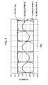
- Fig. 4 is a view illustrating voltage waveforms of operation points A, B, C, and D of the crystal oscillation circuit according to an embodiment.
- Fig. 5 is a comparative view illustrating phase noise characteristic of the crystal oscillation circuit according to the embodiment and the crystal oscillation circuit according to the related art.
- Fig. 6 is a view illustrating the relationship between an output level set and an output waveform of an output terminal in the crystal oscillation circuit according to the embodiment.
- Fig. 7 is a circuit diagram illustrating a crystal oscillation circuit according to another embodiment of the invention.
- Fig. 8 is a circuit diagram illustrating a crystal oscillation circuit according to related art.
- Fig. 9 is a circuit diagram illustrating a crystal oscillation circuit proposed beforehand by the applicant of the invention.
- Fig. 1 is a circuit diagram illustrating a crystal oscillation circuit serving as a piezoelectric oscillation circuit according to an embodiment of the invention.
- reference numeral A represents an output terminal of an oscillation amplification circuit
- reference numeral B represents an output terminal of a first buffer circuit 2
- reference numeral C represents an output terminal of a second buffer circuit 3.
- An output line of a stabilized power supply 6 is connected to a gate of a depletion type MOS transistor M11 and each source of a Pch-CMOS transistor M1 of the oscillation amplification circuit 1, a Pch-CMOS transistor M3 of the first buffer circuit 2, and a Pch-CMOS transistor M5 of the second buffer circuit 3, respectively.
- this embodiment shows an example that the oscillation amplification circuit 1 is configured by using an inverter amplifier.
- the embodiment is not limited to the inverter circuit but the oscillation amplification circuit 1 may be configured by using, for example, a bipolar transistor.
- a DC-blocking capacitor should be inserted to an input part of the first buffer circuit 2 indicated by point A in Fig. 1 and a feedback bias resistor having high-resistance should be inserted between input and output parts.
- an output line of a DC power supply VDD is connected to the drain of the depletion type MOS transistor M11 and a drain of an Nch-MOS transistor M9.
- An inverter output signal output from the third buffer circuit 4 is DC blocked by capacitors CB1 and CB2 and applied to gates of the Nch-MOS transistor M9 and the Pch-CMOS transistor M10 of an output amplification circuit 5 connected to the other ends of the capacitors CB1 and CB2, respectively.
- the voltage at point D that is, a gate voltage VG M9 of the Nch-MOS transistor M9, is determined by dividing the resistance of resistors R1 and RD1 to RD3. If the Nch-MOS transistor M9 is turned on, the voltage VGS between the gate sources of the Pch-CMOS transistor M10 becomes low to be cut off.
- Fig. 2 is a view illustrating the relationship between an oscillation frequency and the power supply in the crystal oscillation circuit according to this embodiment.
- Fig. 3 is a view illustrating the relationship between an output level and the power supply. As can be seen in Figs. 2 and 3, in the crystal oscillation circuit according to this embodiment, since the high frequency accuracy can be obtained within a wide range of the DC voltage Vdd, it is understood that the oscillation output level is extremely stable.
- the DC power supply VDD supplies a current to be supplied from the output amplification circuit 5 to a load capacitor connected to an output terminal (OUT terminal) and a current to be supplied from the third buffer circuit 4 to the capacitors CB1 and CB2 without using the stabilized power supply 6.
- Fig. 5 is a comparative view illustrating the phase noise characteristic of the crystal oscillation circuit according to this embodiment and the crystal oscillation circuit according to the related art.
- the crystal oscillation circuit according to this embodiment shown in Fig. 5 it is possible to improve the phase noise characteristic by about 10 dB in a detuning frequency which is more than 10 kHz.
- the crystal oscillation circuit provides MOS switches MSW1, MSW2, and MSW3 serving as the output level adjustment circuit which adjusts the output level by varying the gate voltage of the Nch-CMOS transistor M9 forming the output amplification circuit 5, as shown in Fig. 1.
- the MOS switches MSW1, MSW2, and MSW3 are provided between a connection point of the resistors RD1 and RD2 and a ground potential, between a connection point of the resistors RD2 and RD3 and a ground potential, and between the resistors RD3 and a ground potential, respectively.
- a decoder 12 decodes the data stored in the memory circuit 11 so as to determine the switch to be turned on.
- the voltage at the point D is obtained by dividing the resistance of the resistors R1 and RD1.
- the resistor RD1 is set to have a resistance ratio in which a voltage of about 0.2 V drops.
- the resistors RD1 to RD3 are respectively set so that the output amplitude becomes 1.0 Vp-p when the MOS switch MSW2 is selected, and so that the output amplitude becomes 1.2 Vp-p when the MOS switch MSW3 is selected. That is, the output level becomes a set1 (Min set) when selecting the MOS switch MSW1, the output level becomes a set2 (Typ set) when selecting the MOS switch MSW2, and the output level becomes a set3 (Max set) when selecting the MOS switch MSW1.
- Fig. 6 shows an output waveform in accordance with each of the output level sets selected.
- the crystal oscillation circuit it is possible to arbitrarily adjust the oscillation output amplitude by storing information for selecting a desired resistor among the divided resistors RD1 to RD3 and setting the selected resistor to a desired output level in the memory circuit 11 and electrically conducting or electrically disconnecting the desired MOS switch in accordance with an analog signal decoded by the decoder 12 based on the information stored in the memory circuit 11.
- the crystal oscillation circuit 11 when shipping the crystal oscillation circuit as a real oscillator, the information stored in the memory circuit 11 should be determined beforehand and the output level thereof may not be arbitrarily selected after the shipping.
- the output level can be selected with the three stages but it is only an example.
- the output level can be selected with various stages other than the three stages by increasing the number of resistors RD and the number of MOS switches corresponding to the resistors RD.
- Fig. 7 is a circuit diagram illustrating a crystal oscillation circuit according to another embodiment of the invention.
- the output level can be selected through five stages.
- the output level becomes a set1 (Min set) when selecting the MOS switch MSW1
- the output level becomes a set3 (Typ set) when selecting the MOS switch MSW3
- the output level becomes a set5 (Max set) when selecting the MOS switch MSW3.
- the circuit configured to bypass the connection points of the resistors RD1 to RD5 and grounds by using the MOS switch has been described. However, it can be configured to bypass the connection point of the MOS transistor M9 and a gate by the MOS switch.
- the crystal oscillation circuit shown in Figs. 1 and 7 as a circuit configuration for adjusting the voltage between the gate of the MOS transistor M9 and the ground, a circuit including the MOS switch so as to adjust a value of resistance between the gate of the MOS transistor M9 and the ground has been described. While providing a resistive network connecting a plurality of resistors in series instead of the resistor R1 shown in Figs. 1 and 7, the crystal oscillation circuit can be configured with a MOS switch which bypasses between the connection points of the resistors and the stabilized power supply 6 or between the connection points of the resistors and the gate of the MOS transistor M9, a decoder for controlling to turn on/off the MOS switch, and a memory.
- the crystal oscillation circuit can be configured by controlling the value of the resistance between the gate of the MOS transistor M9 and the ground while controlling the value of the resistance between the gate of the MOS transistor M9 and the stabilized power supply 6. In this case, it is possible to precisely adjust a gate potential of the MOS transistor M9.
Landscapes
- Oscillators With Electromechanical Resonators (AREA)
Applications Claiming Priority (1)
| Application Number | Priority Date | Filing Date | Title |
|---|---|---|---|
| JP2005133547A JP4259485B2 (ja) | 2005-04-28 | 2005-04-28 | 圧電発振回路 |
Publications (2)
| Publication Number | Publication Date |
|---|---|
| EP1720246A2 true EP1720246A2 (de) | 2006-11-08 |
| EP1720246A3 EP1720246A3 (de) | 2008-01-23 |
Family
ID=36691589
Family Applications (1)
| Application Number | Title | Priority Date | Filing Date |
|---|---|---|---|
| EP06008778A Withdrawn EP1720246A3 (de) | 2005-04-28 | 2006-04-27 | Piezoelektrische Oszillatorschaltung |
Country Status (6)
| Country | Link |
|---|---|
| US (1) | US20060244546A1 (de) |
| EP (1) | EP1720246A3 (de) |
| JP (1) | JP4259485B2 (de) |
| KR (1) | KR100750781B1 (de) |
| CN (1) | CN1855693A (de) |
| TW (1) | TWI309919B (de) |
Families Citing this family (25)
| Publication number | Priority date | Publication date | Assignee | Title |
|---|---|---|---|---|
| JP2008103841A (ja) * | 2006-10-17 | 2008-05-01 | Matsushita Electric Ind Co Ltd | 水晶発振回路 |
| KR100884603B1 (ko) * | 2007-05-09 | 2009-02-19 | 주식회사 하이닉스반도체 | 반도체소자의 버퍼장치 |
| JP2009111722A (ja) * | 2007-10-30 | 2009-05-21 | Panasonic Corp | 発振制御装置及び発振器 |
| JP5061857B2 (ja) * | 2007-11-12 | 2012-10-31 | セイコーエプソン株式会社 | 圧電発振器 |
| US7868710B1 (en) * | 2009-02-04 | 2011-01-11 | Rf Micro Devices, Inc. | Digitally-controlled crystal oscillator circuit |
| DE102010011757B4 (de) * | 2010-03-17 | 2017-08-17 | Texas Instruments Deutschland Gmbh | Elektronische Vorrichtung zum Zwischenspeichern von Signalen eines temperaturkompensierten Quarzoszillators |
| TWI423729B (zh) * | 2010-08-31 | 2014-01-11 | Au Optronics Corp | 整合放大器的源級驅動器 |
| TW201225540A (en) * | 2010-12-14 | 2012-06-16 | Askey Computer Corp | Multiple-output clock source signal generator |
| US9294251B2 (en) | 2011-02-08 | 2016-03-22 | Nippon Telegraph And Telephone Corporation | Wireless communication system, transmitting device, receiving device, and wireless communication method |
| JP2012182764A (ja) * | 2011-03-03 | 2012-09-20 | Seiko Epson Corp | 発振器 |
| JP2012257183A (ja) * | 2011-06-10 | 2012-12-27 | Mitsumi Electric Co Ltd | 発振回路 |
| CN103036561B (zh) * | 2011-09-28 | 2015-09-16 | 华晶科技股份有限公司 | 时脉供应装置及其方法 |
| JP6234008B2 (ja) * | 2012-03-28 | 2017-11-22 | セイコーエプソン株式会社 | 発振回路及び電子機器 |
| JP5549714B2 (ja) * | 2012-08-08 | 2014-07-16 | セイコーエプソン株式会社 | 発振用回路 |
| JP5533968B2 (ja) * | 2012-09-26 | 2014-06-25 | セイコーエプソン株式会社 | 温度補償型発振器および電子機器 |
| JP5622120B2 (ja) * | 2012-09-27 | 2014-11-12 | セイコーエプソン株式会社 | バッファ回路 |
| JP5477492B2 (ja) * | 2013-03-27 | 2014-04-23 | セイコーエプソン株式会社 | 圧電発振器 |
| JP6352042B2 (ja) * | 2013-06-28 | 2018-07-04 | エイブリック株式会社 | 遅延回路、発振回路及び半導体装置 |
| JP2016119550A (ja) * | 2014-12-19 | 2016-06-30 | ファナック株式会社 | 水晶発振器 |
| JP6561487B2 (ja) * | 2015-02-16 | 2019-08-21 | セイコーエプソン株式会社 | 発振回路、発振器、電子機器および移動体 |
| CN104714325B (zh) * | 2015-03-18 | 2017-09-19 | 深圳市华星光电技术有限公司 | 液晶显示器及其制备方法 |
| US9444435B1 (en) * | 2015-10-20 | 2016-09-13 | Stmicroelectronics S.R.L. | Injection locked ring oscillator circuit with an analog quadrature calibration loop |
| JP7669779B2 (ja) * | 2021-04-30 | 2025-04-30 | セイコーエプソン株式会社 | 回路装置及び発振器 |
| US11764730B2 (en) | 2021-05-06 | 2023-09-19 | Nordic Semiconductor Asa | Oscillator circuits |
| JP2024136547A (ja) * | 2023-03-24 | 2024-10-04 | セイコーエプソン株式会社 | 回路装置、発振器 |
Family Cites Families (14)
| Publication number | Priority date | Publication date | Assignee | Title |
|---|---|---|---|---|
| DE19738718A1 (de) * | 1997-09-04 | 1999-03-25 | Siemens Ag | Oszillatorschaltung mit einem Schwingquarz |
| US6738601B1 (en) * | 1999-10-21 | 2004-05-18 | Broadcom Corporation | Adaptive radio transceiver with floating MOSFET capacitors |
| US6359489B1 (en) * | 2000-10-05 | 2002-03-19 | Silicon Integrated Systems Corp. | Clock signal generation and buffer circuit having high noise immunity and low power consumption |
| US7177610B2 (en) * | 2001-01-12 | 2007-02-13 | Silicon Laboratories Inc. | Calibrated low-noise current and voltage references and associated methods |
| JP2002261545A (ja) * | 2001-03-02 | 2002-09-13 | Nippon Dempa Kogyo Co Ltd | 低電圧発振回路 |
| US6995623B2 (en) * | 2001-08-16 | 2006-02-07 | Toyo Communication Equipment Co., Ltd. | Piezoelectric oscillator |
| JP2003338710A (ja) * | 2001-11-02 | 2003-11-28 | Seiko Epson Corp | 発振器およびこれを用いた電子機器 |
| JP2003258553A (ja) | 2002-02-28 | 2003-09-12 | Kawasaki Microelectronics Kk | 発振回路 |
| US6707722B2 (en) * | 2002-07-23 | 2004-03-16 | Micron Technology, Inc. | Method and apparatus for regulating predriver for output buffer |
| US20040032300A1 (en) * | 2002-08-19 | 2004-02-19 | Koninklijke Philips Electronics N.V. | Multi-phase oscillator and method therefor |
| JP4259241B2 (ja) | 2003-09-10 | 2009-04-30 | セイコーエプソン株式会社 | 発振回路及び半導体集積回路 |
| KR20050033145A (ko) * | 2003-10-06 | 2005-04-12 | 주식회사 엘리아테크 | 주파수 조절이 가능한 저전압 발진회로 |
| KR100489837B1 (ko) * | 2003-10-08 | 2005-05-16 | 삼성전기주식회사 | 다중 레벨 전압 제어 발진기 |
| US7123109B2 (en) * | 2004-12-15 | 2006-10-17 | Intel Corporation | Crystal oscillator with variable bias generator and variable loop filter |
-
2005
- 2005-04-28 JP JP2005133547A patent/JP4259485B2/ja not_active Expired - Fee Related
-
2006
- 2006-04-25 CN CNA2006100769033A patent/CN1855693A/zh active Pending
- 2006-04-27 EP EP06008778A patent/EP1720246A3/de not_active Withdrawn
- 2006-04-27 US US11/413,146 patent/US20060244546A1/en not_active Abandoned
- 2006-04-27 TW TW095115035A patent/TWI309919B/zh not_active IP Right Cessation
- 2006-04-28 KR KR1020060038687A patent/KR100750781B1/ko not_active Expired - Fee Related
Also Published As
| Publication number | Publication date |
|---|---|
| KR100750781B1 (ko) | 2007-08-20 |
| EP1720246A3 (de) | 2008-01-23 |
| JP4259485B2 (ja) | 2009-04-30 |
| JP2006311379A (ja) | 2006-11-09 |
| KR20060113532A (ko) | 2006-11-02 |
| US20060244546A1 (en) | 2006-11-02 |
| CN1855693A (zh) | 2006-11-01 |
| TWI309919B (en) | 2009-05-11 |
| TW200701627A (en) | 2007-01-01 |
Similar Documents
| Publication | Publication Date | Title |
|---|---|---|
| EP1720246A2 (de) | Piezoelektrische Oszillatorschaltung | |
| US7852164B2 (en) | Piezoelectric oscillator | |
| KR101232407B1 (ko) | 이득 확장 스테이지를 가진 증폭기 | |
| US8736391B2 (en) | Method to shorten crystal oscillator's startup time | |
| US7042299B2 (en) | Crystal oscillation circuit | |
| WO2007095451A1 (en) | High gain, high frequency cmos oscillator circuit and method | |
| US7348859B2 (en) | Crystal oscillator | |
| US6859103B2 (en) | Bias circuit for improving linearity of a radio frequency power amplifier | |
| US20080238561A1 (en) | Piezoelectric oscillator | |
| EP1604453A1 (de) | Amplitudenpegelsteuerschaltung für einen oszillator | |
| JP7089239B2 (ja) | 発振回路 | |
| US6836190B2 (en) | Oscillator device and electronic apparatus using the same | |
| JP2007053746A (ja) | 集積回路 | |
| JP4244890B2 (ja) | 圧電発振回路 | |
| US6717483B2 (en) | Low cost voltage controlled crystal oscillator (VCXO) | |
| US8035455B1 (en) | Oscillator amplitude control network | |
| US7515001B2 (en) | AC amplifier and piezoelectric vibrator oscillator | |
| JP2011244064A (ja) | 水晶発振器 | |
| JP3778596B2 (ja) | 同調増幅回路 | |
| JP3591691B2 (ja) | 半導体集積回路装置 | |
| JP2006005558A (ja) | 高周波発振器 | |
| JP2005260797A (ja) | 電圧制御発振器 | |
| JPH0786834A (ja) | 発振回路装置 | |
| JP2004254071A (ja) | 増幅回路 | |
| KR20010063224A (ko) | 온도 보상형 발진회로 |
Legal Events
| Date | Code | Title | Description |
|---|---|---|---|
| PUAI | Public reference made under article 153(3) epc to a published international application that has entered the european phase |
Free format text: ORIGINAL CODE: 0009012 |
|
| AK | Designated contracting states |
Kind code of ref document: A2 Designated state(s): AT BE BG CH CY CZ DE DK EE ES FI FR GB GR HU IE IS IT LI LT LU LV MC NL PL PT RO SE SI SK TR |
|
| AX | Request for extension of the european patent |
Extension state: AL BA HR MK YU |
|
| PUAL | Search report despatched |
Free format text: ORIGINAL CODE: 0009013 |
|
| AK | Designated contracting states |
Kind code of ref document: A3 Designated state(s): AT BE BG CH CY CZ DE DK EE ES FI FR GB GR HU IE IS IT LI LT LU LV MC NL PL PT RO SE SI SK TR |
|
| AX | Request for extension of the european patent |
Extension state: AL BA HR MK YU |
|
| 17P | Request for examination filed |
Effective date: 20080718 |
|
| 17Q | First examination report despatched |
Effective date: 20080825 |
|
| AKX | Designation fees paid |
Designated state(s): DE FI FR GB |
|
| STAA | Information on the status of an ep patent application or granted ep patent |
Free format text: STATUS: THE APPLICATION IS DEEMED TO BE WITHDRAWN |
|
| 18D | Application deemed to be withdrawn |
Effective date: 20081205 |